SinoTechIntel Academic Portal
🏛️ Indexed Academic JournalImpact Factor: 3.8

Journal of Semiconductors (半导体学报 - 中国科学院半导体研究所)

Authoritative peer-reviewed journal in materials science, metallurgy, chemistry and engineering technologies: Journal of Semiconductors (半导体学报 - Viện Bán dẫn CAS)

Total Research Papers: 115
Access: 100% Free Open Access
Browse by Publication Year & Volume

Published Research Papers

Showing 115 of 115 peer-reviewed papers with full Graphical Abstracts.

Original ResearchVol. 32, Issue 2 • pp. 100-112DOI: 10.1088/1674-4926/26020002Jan 15, 2026

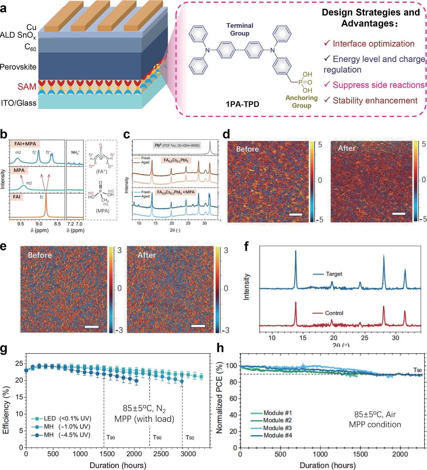
Mitigating Phosphonic Acid–Perovskite Interfacial Degradation via Molecular Engineering for Ultra-Stable Solar Cells

Authors: LI Xu, GUO Yuxiao, LUO Xin, YAN Haoyuan, XU Bo

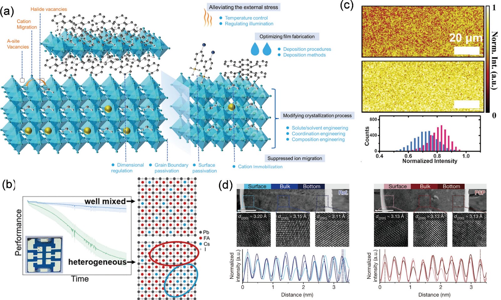
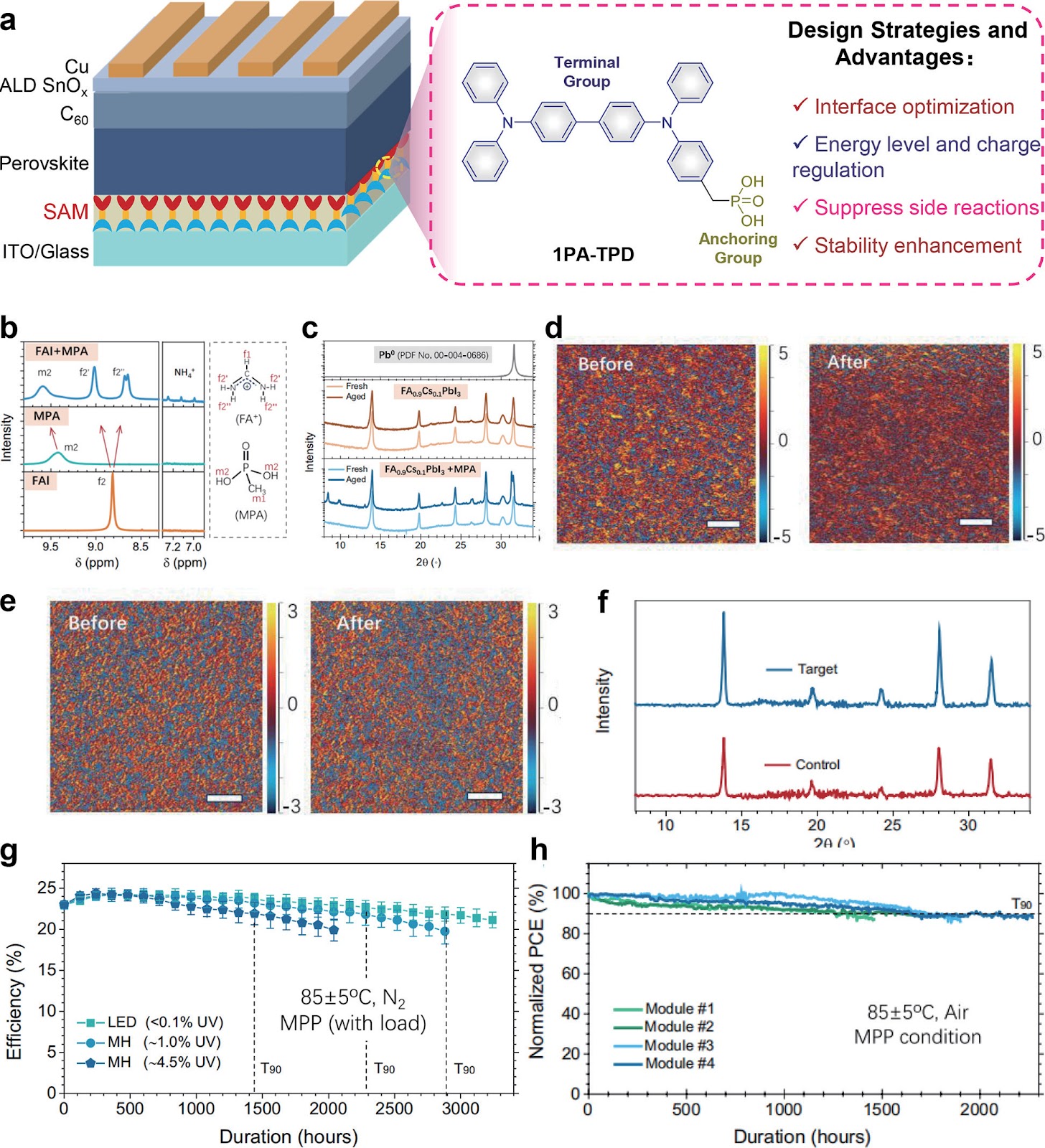
Metal halide perovskite solar cells (PSCs) have emerged as a leading next-generation photovoltaic technology, with certified efficiencies surpassing 27% and approaching the theoretical limit for single-junction devices. However, their commercialization is critically hindered by insufficient long-term operational stability, particularly under harsh conditions such as elevated temperatures (≥85 °C) and full-spectrum illumination. The hole-transport layer (HTL) plays a decisive role in both efficiency and stability, and phosphonic acid-based self-assembled monolayers (PA-SAMs) have become the material of choice for inverted-structure PSCs due to their molecular-scale precision and superior energy-level alignment. Nevertheless, PA-SAMs primarily anchor to ITO surfaces via weak hydrogen bonds, which dissociate under photothermal stress, leading to molecular desorption and migration into the perovskite layer, thereby inducing degradation and performance decline. In a recent breakthrough published in Science (2026), Fei et al. report a transformative molecular engineering strategy that unlocks ultra-stable PSCs. They designed a triphenylamine-based phosphonic acid (1PA-TPD) with robust covalent anchoring to ITO substrates and optimized a mixed SAM system (60 wt% 1PA-TPD + 40 wt% EtCz3EPA), successfully suppressing interfacial reactivity between PA-SAMs and perovskites. This multifunctional strategy integrates strong substrate binding, interfacial reaction inhibition, crystallinity enhancement, and defect passivation, enabling small-area PSCs with a power conversion efficiency (PCE) of 25.0% and a T90 lifetime of nearly 3000 hours, as well as minimodules with >22% PCE and ~2200 hours T90 under harsh photothermal conditions. This work deciphers a previously underappreciated degradation pathway and provides a universal design principle for stable interfacial layers, marking a critical step toward PSC commercialization.
Mitigating Phosphonic Acid–Perovskite Interfacial Degradation via Molecular Engineering for Ultra-Stable Solar Cells
Graphical Abstract
Original ResearchVol. 32, Issue 2 • pp. 100-112DOI: 10.1088/1674-4926/26020050Jan 15, 2026

Crystallization-Sequence Engineering Enables Organic Solar Cell Modules with Efficiencies Exceeding 18%

Authors: Yunhao Cai, Hui Huang

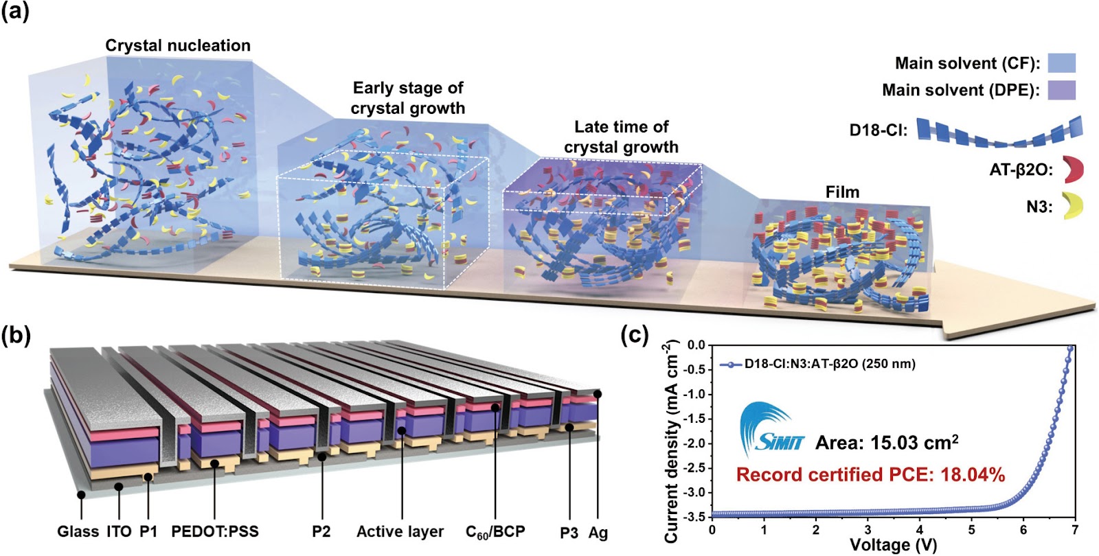
Organic solar cells (OSCs) have emerged as a promising photovoltaic technology due to their mechanical flexibility, low density, and compatibility with solution-based fabrication, enabling applications such as wearable electronics and building-integrated photovoltaics. Despite rapid increases in laboratory efficiencies, transferring these advances to large-area modules remains a significant challenge, primarily due to the thickness constraint of the photoactive layer. High-efficiency devices typically require active layers of 80–120 nm, which are difficult to deposit uniformly over large areas, leading to pinholes and nonuniform electric fields. Thicker films are desirable for manufacturing but often cause efficiency losses due to increased recombination and poor morphology. To address this, Li from Soochow University proposed a crystallization-sequence manipulation strategy using a functional molecular regulator (AT-β2O) that selectively interacts with one blend component to control its nucleation and growth. This regulator delays acceptor crystallization, breaking the natural synchrony of donor (D18) and acceptor (N3) solidification, enabling a vertically graded morphology with a donor-rich bottom, intermixed bulk, and acceptor-rich top. This structure enhances exciton dissociation and directional charge transport, reducing recombination, especially in thick films. Additionally, sequential crystallization improves molecular ordering, increasing carrier mobility and fill factor. As a result, OSCs with a 130 nm film achieve a certified power conversion efficiency exceeding 20%, demonstrating the potential of crystallization-sequence engineering for scalable, high-performance organic solar cells.

Crystallization-Sequence Engineering Enables Organic Solar Cell Modules with Efficiencies Exceeding 18%
Graphical Abstract
Original ResearchVol. 32, Issue 1 • pp. 100-112DOI: 10.1088/1674-4926/26010031Jan 15, 2026

Band Engineering Solar-Blind Ultraviolet Photodetectors: Breaking the Sensitivity-Speed Trade-off

Authors: HONG Bin Wang, PENG Li, JIANGANG Ma

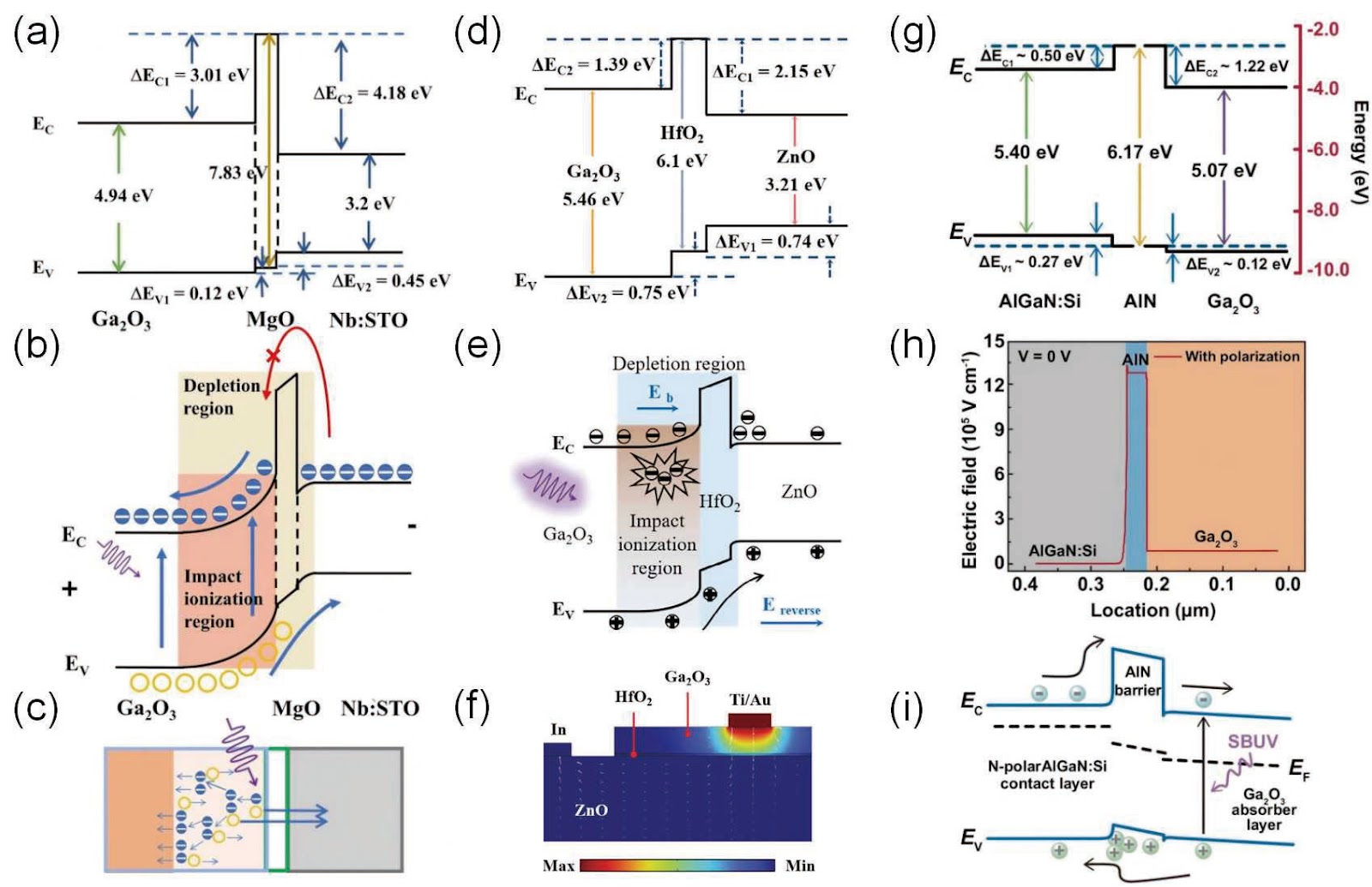
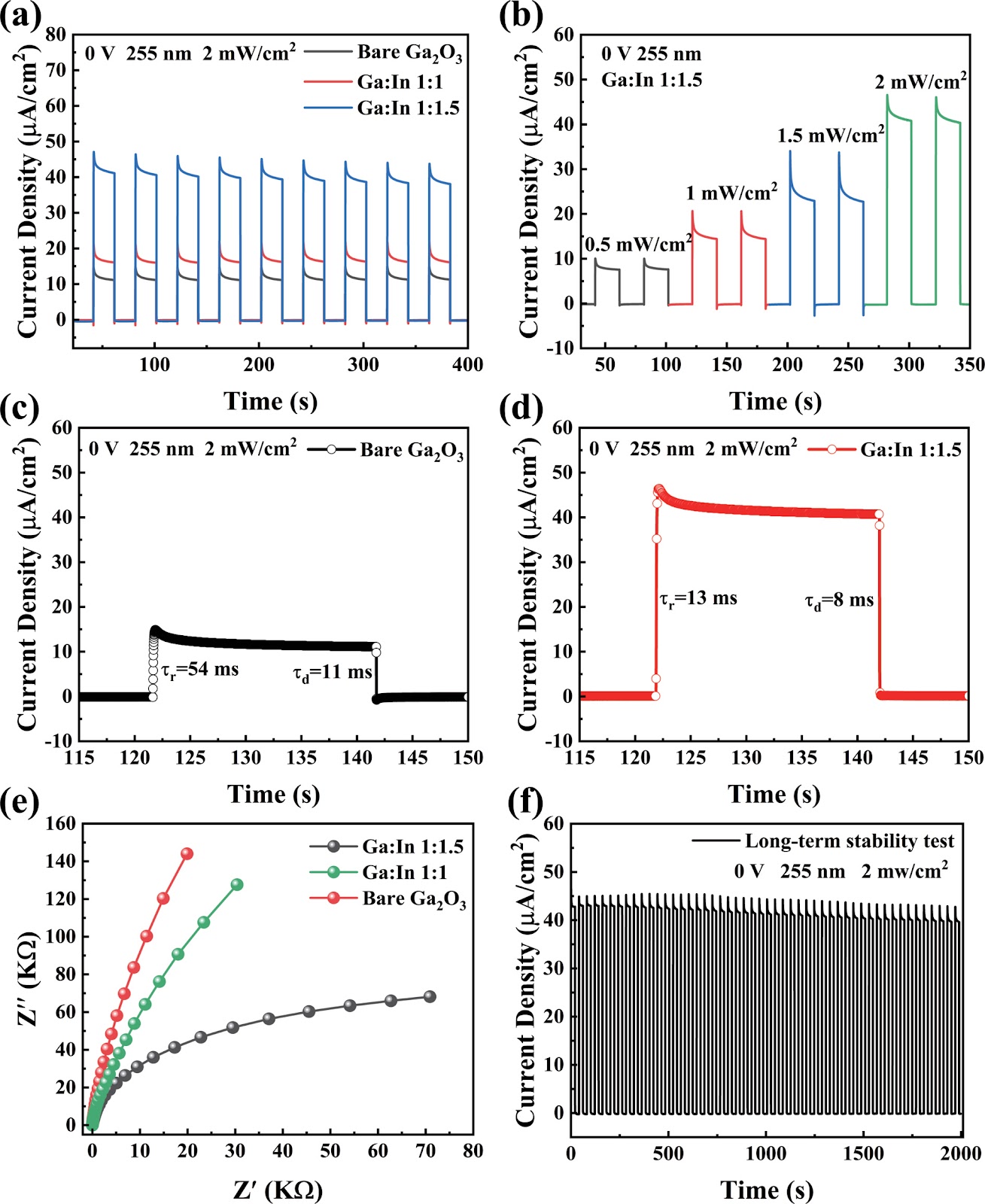
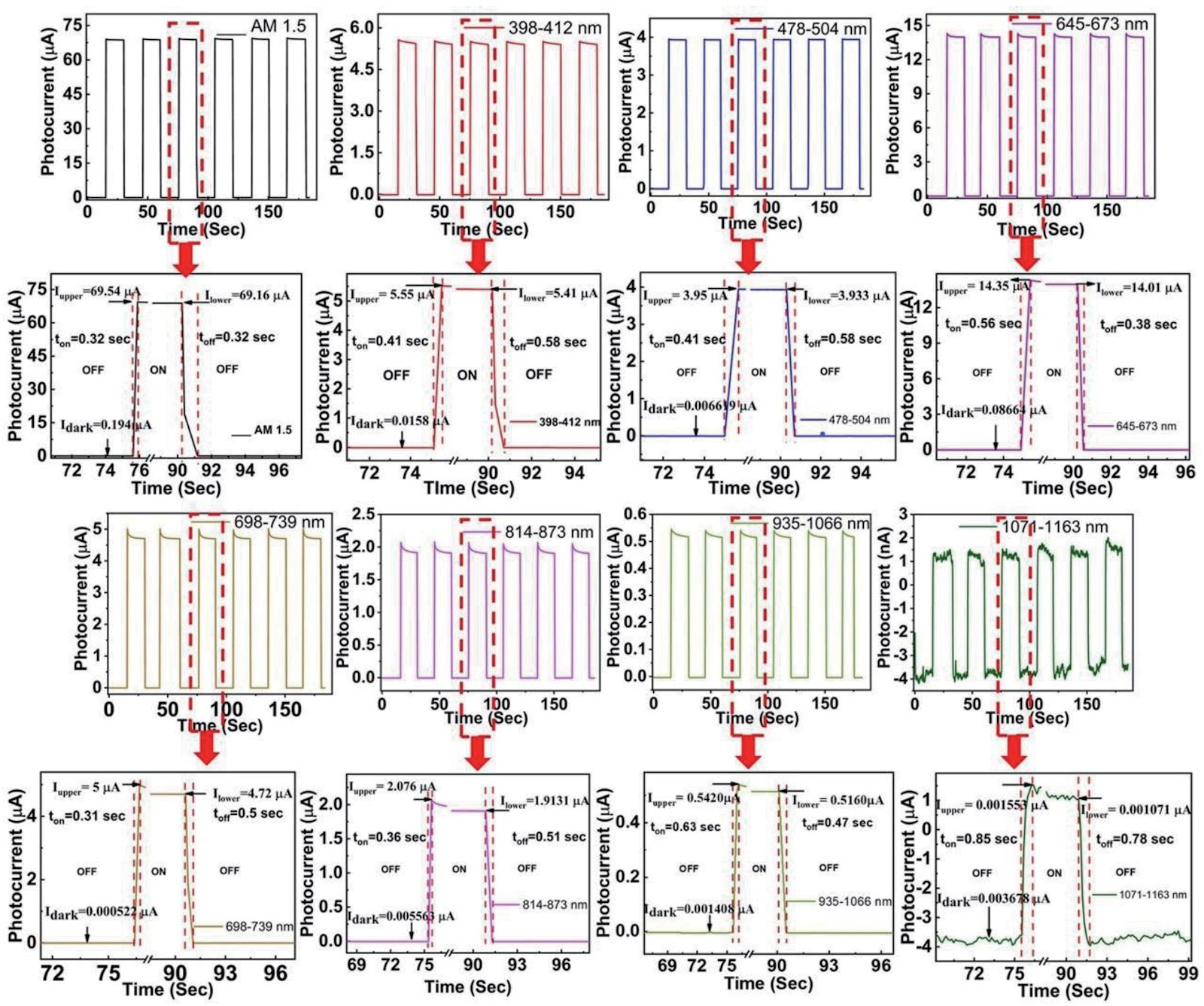
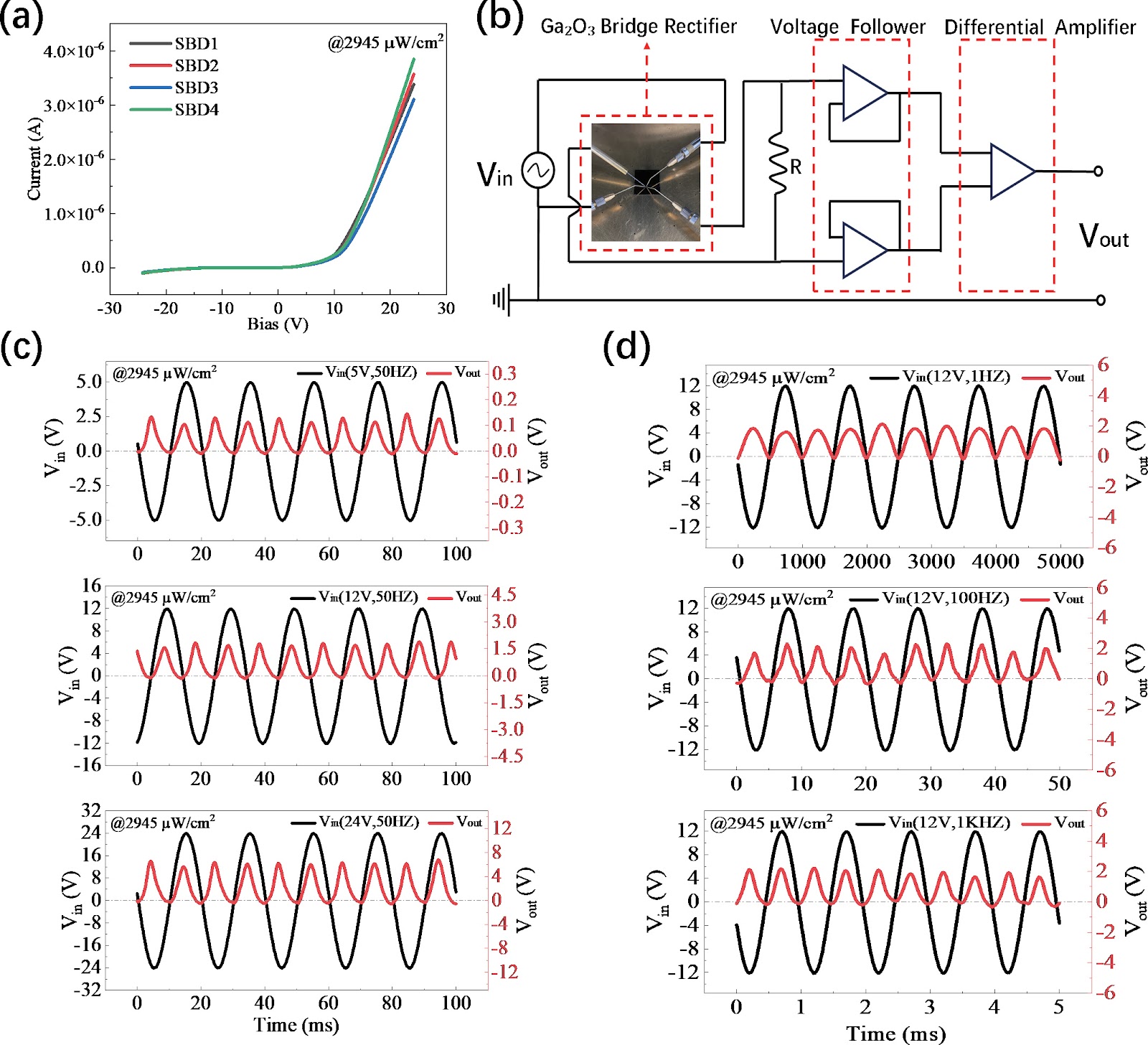
Solar-blind ultraviolet (UV) photodetectors are crucial for applications requiring high signal-to-noise ratio and immunity to solar background noise. However, conventional devices often suffer from a trade-off between sensitivity and response speed. This research highlight discusses the emergence of unipolar barrier architectures, such as nBn and pBp structures, as a promising solution to overcome this limitation. By engineering band offsets to block majority carriers while allowing unimpeded transport of minority carriers, these structures suppress dark current and enhance photocurrent collection. Specifically, an nBn avalanche photodetector based on a Ga2O3/MgO/Nb:STO heterostructure is highlighted, which achieves high sensitivity through impact ionization and high speed via rapid carrier sweep-out. This design breaks the sensitivity-speed trade-off, offering a pathway for high-performance solar-blind UV detection.

Band Engineering Solar-Blind Ultraviolet Photodetectors: Breaking the Sensitivity-Speed Trade-off
Graphical Abstract
Original ResearchVol. 32, Issue 1 • pp. 100-112DOI: 10.1088/1674-4926/26010049Jan 15, 2026

θ-TaN: Redefining the Thermal Conductivity Limit of Metallic Materials

Authors: Miao-Ling Lin, Ping-Heng Tan

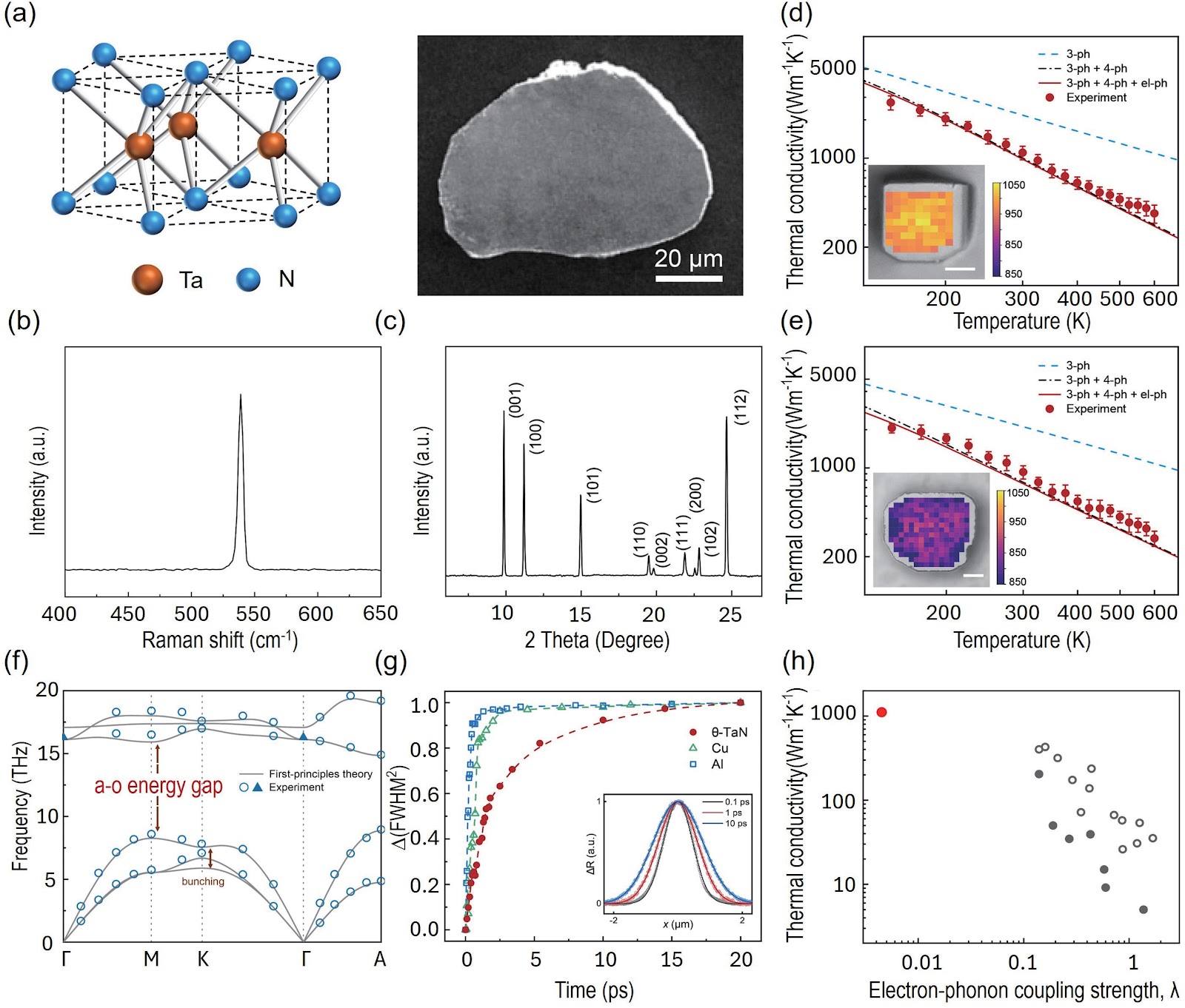
Thermal management has become a critical bottleneck for the performance and reliability of modern electronics. For over a century, the thermal conductivity (κ) of metallic materials was believed to have an inherent upper limit of approximately 400 W·m⁻¹·K⁻¹, constrained by strong electron-phonon coupling and lattice anharmonicity. However, a groundbreaking study by Li et al. (Science, 2026) experimentally realized single-crystalline θ-phase tantalum nitride (θ-TaN), a metastable transition metal nitride with a room-temperature thermal conductivity of ~1100 W·m⁻¹·K⁻¹ along the a-axis and ~928 W·m⁻¹·K⁻¹ along the c-axis, nearly three times that of copper. This work shatters the long-standing thermal conductivity limit for metals and validates theoretical predictions. The exceptional performance of θ-TaN arises from its unique hexagonal crystal structure (space group P6m2), featuring a large acoustic-optical phonon gap (~8 THz) and acoustic phonon bunching, which suppress phonon-phonon scattering. Additionally, weak electron-phonon coupling and minimal isotope scattering contribute to phonon-dominated heat transport. The authors synthesized high-quality single crystals via a flux-assisted metathesis reaction, overcoming challenges of conventional high-pressure routes. Using time-domain thermoreflectance and inelastic X-ray scattering, they confirmed the intrinsic ultrahigh thermal conductivity and mapped the phonon band structure. This discovery introduces a new class of high-thermal-conductivity metals, opening transformative opportunities for thermal management in electronics, aerospace, and energy systems.

θ-TaN: Redefining the Thermal Conductivity Limit of Metallic Materials
Graphical Abstract
Original ResearchVol. 32, Issue 2 • pp. 100-112DOI: 10.1088/1674-4926/26020027Jan 15, 2026

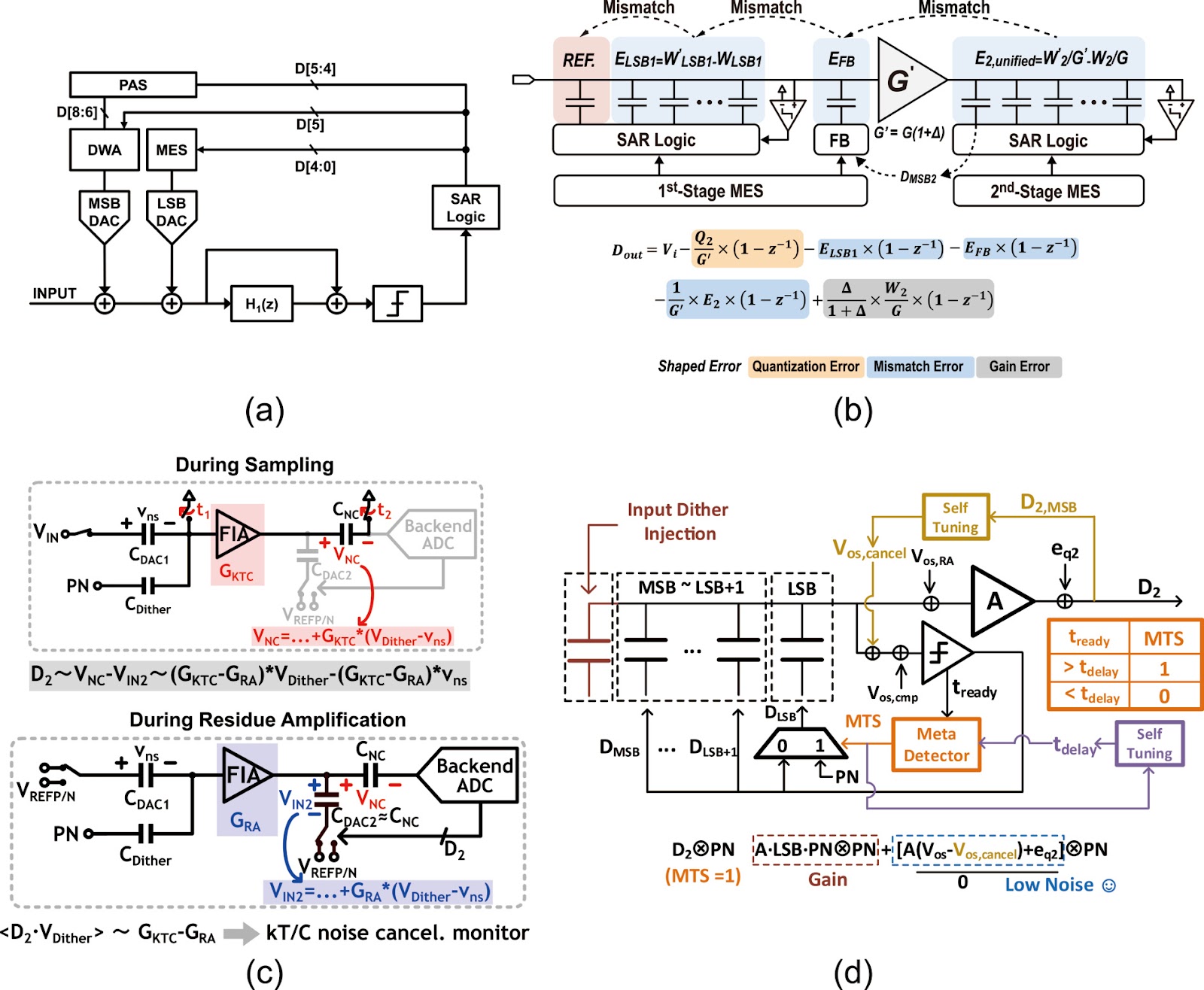
Multi-phase clock generation techniques toward high-frequency and wideband applications

Authors: Junyan Bi, Hao Xu, Na Yan

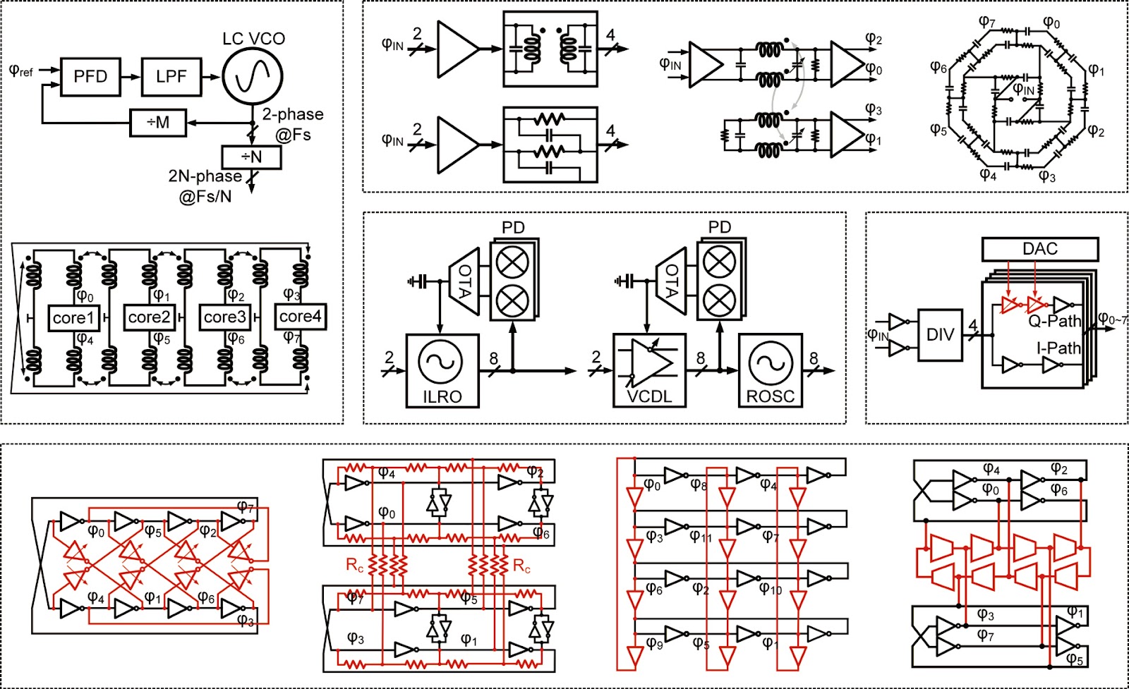
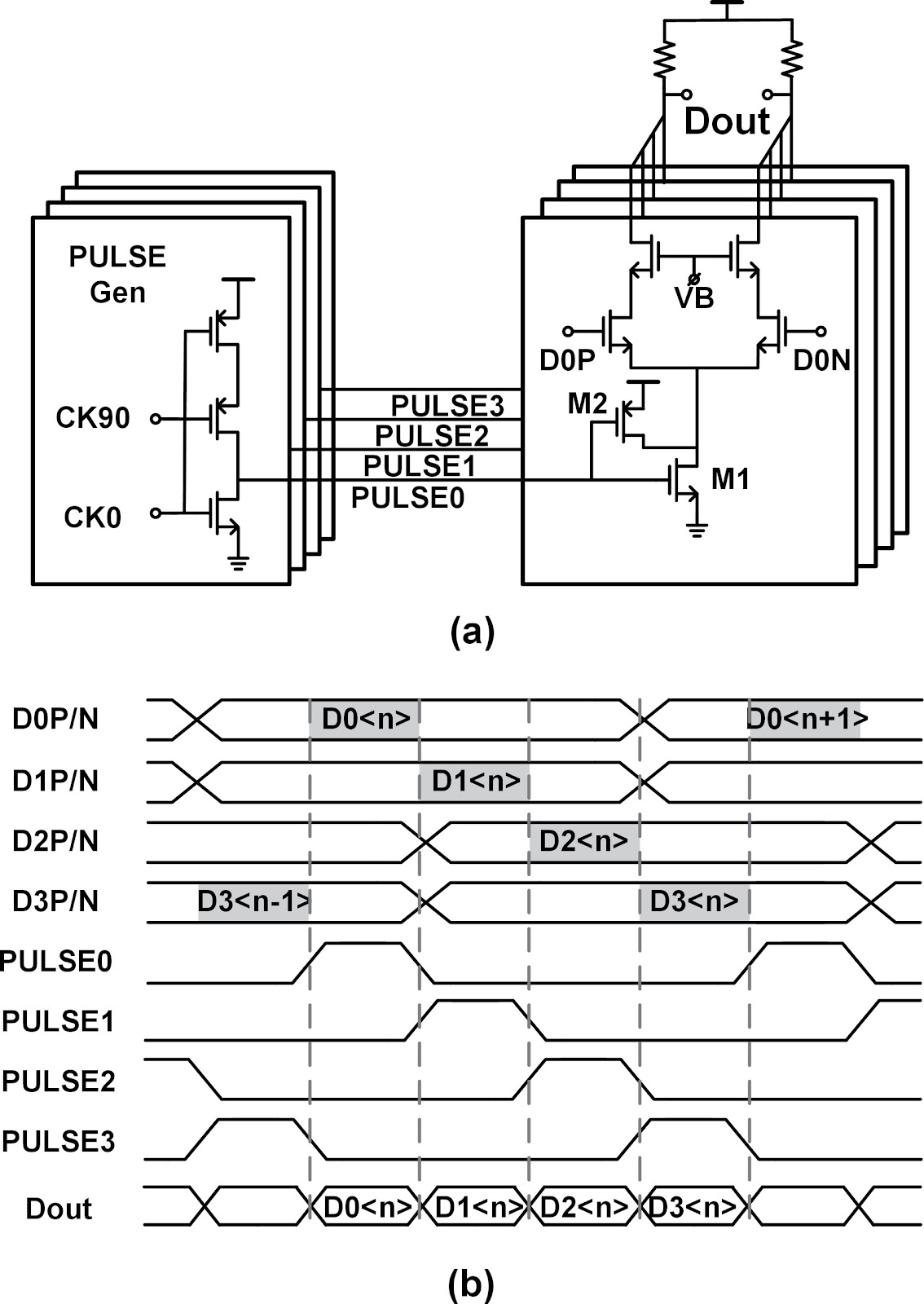
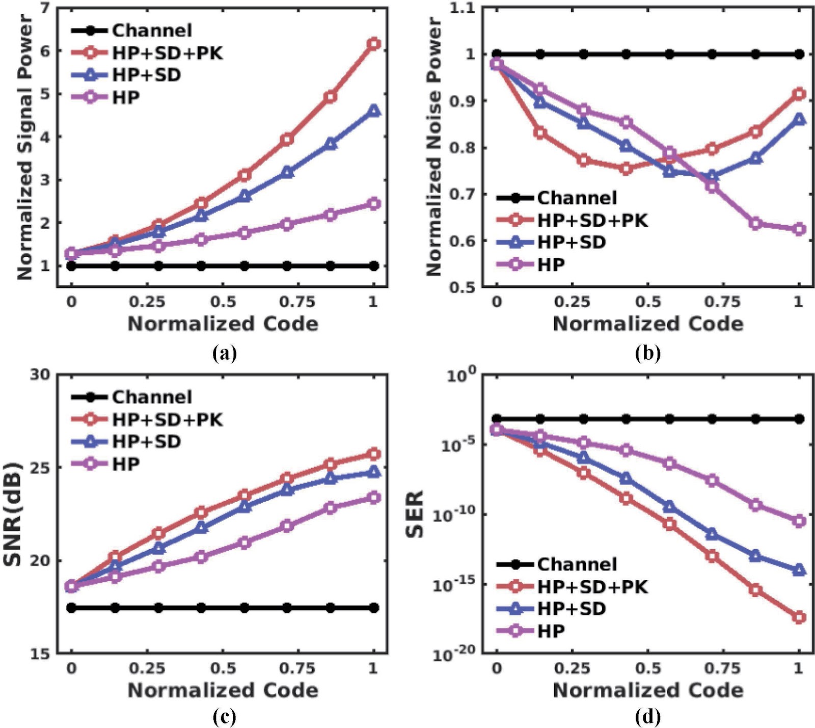
Multi-phase clocks are fundamental components in modern wireline and wireless communication systems, serving as timing and phase references across diverse architectures. As data rates and carrier frequencies scale, the required phase count and operating frequency have increased substantially, pushing conventional clock generation techniques toward their limits. In high-speed wireline transceivers, multi-phase clocks are essential for CDR phase interpolation, time-interleaved ADCs, and advanced PAM-based modulation, imposing stringent requirements on RMS jitter, phase accuracy, and robustness against PVT variations. In wireless and millimeter-wave systems, they are employed for LO generation, quadrature modulation, and beam steering, where phase accuracy often dominates over absolute jitter. Conventional techniques, including PLL-based dividers, multi-core LC oscillators, and passive phase-shifting networks, face scalability challenges at high frequencies, including limited speed, area overhead, narrowband operation, and sensitivity to mismatch. Ring oscillators offer inherent phase scalability and wide tuning range but suffer from poor stability and jitter. Injection-locked ring oscillators (ILROs) enhance stability and phase noise while preserving multi-phase advantages, yet achieving wide locking range and high phase accuracy simultaneously remains challenging. This research highlight reviews these techniques, discusses their limitations, and outlines advanced injection and feedback schemes to overcome these challenges, aiming to guide future developments in high-frequency and wideband multi-phase clock generation.

Multi-phase clock generation techniques toward high-frequency and wideband applications
Graphical Abstract
Original ResearchVol. 32, Issue 2 • pp. 100-112DOI: 10.1088/1674-4926/26020035Jan 15, 2026

Zigzag Domain Walls Unravel the Polarization Switching Puzzle in Wurtzite Ferroelectrics

Authors: Hang Zang, Zhiming Shi, Xiaojuan Sun, Dabing Li

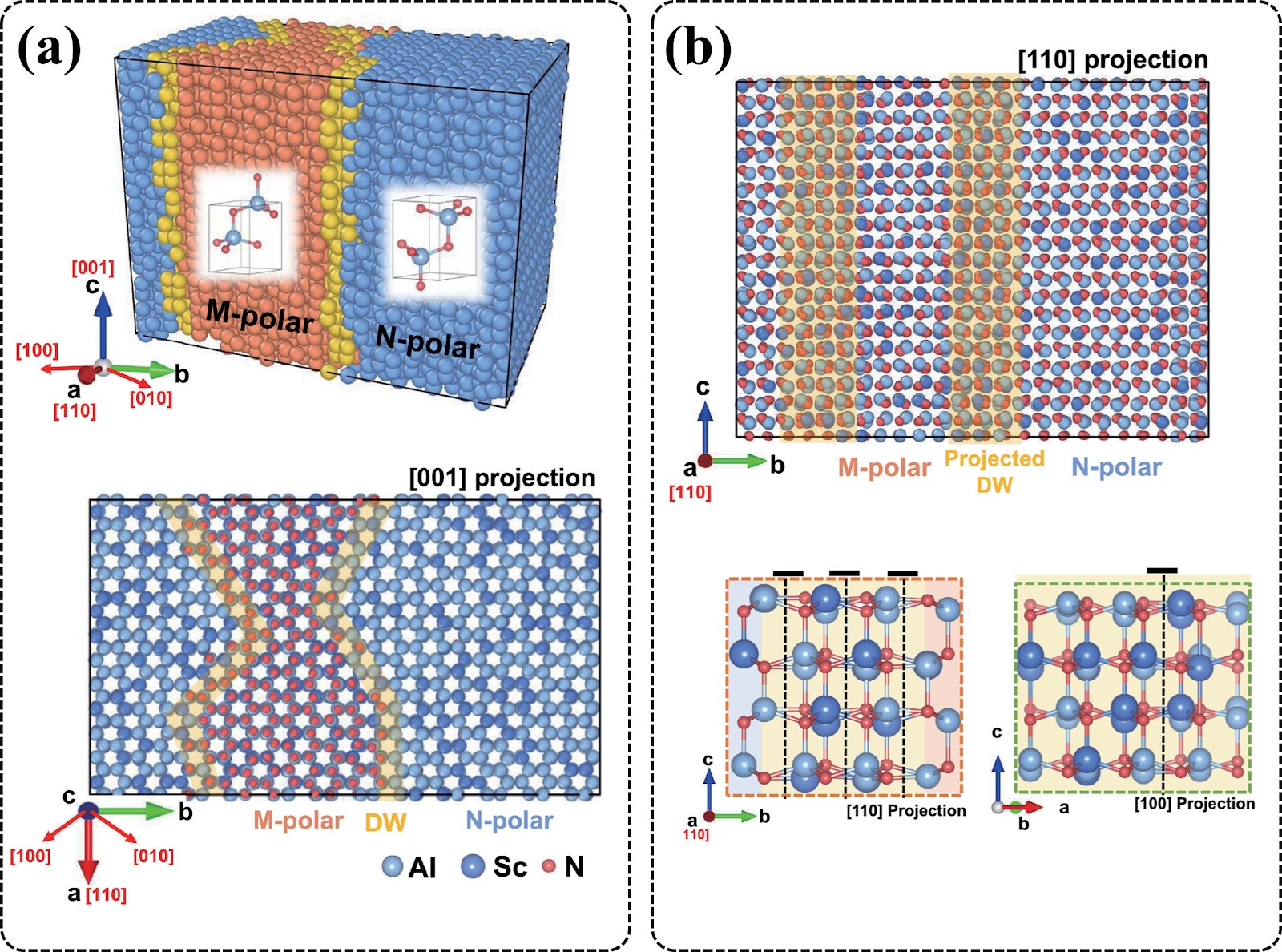
The discovery of robust ferroelectricity in scandium-doped aluminum nitride (Al1−xScxN) has sparked significant interest due to its compatibility with CMOS fabrication, making it a promising candidate for next-generation non-volatile memories and high-frequency devices. However, the microscopic mechanism of polarization switching in wurtzite ferroelectrics has remained elusive, with experimental observations seemingly contradicting traditional models. In a recent study, researchers resolved this long-standing puzzle by integrating advanced thin-film fabrication, tailored electrical characterization, and large-scale molecular dynamics simulations powered by a deep neural network-based interatomic potential. Their findings reveal that the broad 'transitional regions' observed in scanning transmission electron microscopy (STEM) are not a new nonpolar phase but a projection artifact arising from intrinsically three-dimensional zigzag domain walls. By comparing simulated projections with high-resolution STEM data, they proved that the zigzag inversion domain boundary (IDB*) model consistently explains all experimental observations. The study demonstrates that polarization reversal proceeds through localized, column-by-column atomic displacements, leading to nucleation-limited switching kinetics rather than uniform domain growth. Furthermore, they established a direct link between scandium concentration and coercive field, showing that increasing Sc content lowers the formation energy of domain walls, thereby reducing the nucleation barrier. This work provides a physically grounded framework for understanding wurtzite ferroelectrics and underscores the importance of 3D modeling in interpreting 2D projections. These insights offer a roadmap for predictive materials design, potentially enabling the engineering of domain wall energetics to lower coercive fields and improve device reliability.

Zigzag Domain Walls Unravel the Polarization Switching Puzzle in Wurtzite Ferroelectrics
Graphical Abstract
Original ResearchVol. 32, Issue 1 • pp. 100-112DOI: 10.1088/1674-4926/26010050Jan 15, 2026

Bonding at the Atomic Limit: Redefining Contacts in Two-Dimensional Semiconductors

Authors: Bei Zhao, Xidong Duan

Two-dimensional transition metal dichalcogenides (TMDs) hold promise for next-generation electronics, but their industrial adoption is hindered by van der Waals (vdW) contacts, which exhibit weak interfacial coupling and high contact resistance (RC). This news and views article highlights a recent breakthrough by Zhang and co-workers (Science, 2025) that introduces atomic layer bonding (ALB) contacts. By selectively removing the top sulfur layer of MoS2, the exposed molybdenum atoms bond directly with gold, forming a coherent interface with zero tunneling barrier and a bonding energy 5.4 times higher than vdW contacts. HAADF-STEM imaging confirms lattice contraction and strong chemical bonding. Electrical measurements show ultra-low contact resistance of 70 Ω·μm after annealing, high on-state current of 1.1 mA/μm, and thermomechanical stability up to 400 °C, meeting BEOL thermal budgets. ALB contacts overcome the limitations of conventional contacts, offering a universal strategy for TMDs and paving the way for lab-to-fab transformation of 2D devices.

Bonding at the Atomic Limit: Redefining Contacts in Two-Dimensional Semiconductors
Graphical Abstract
Original ResearchVol. 32, Issue 2 • pp. 100-112DOI: 10.1088/1674-4926/26020045Jan 15, 2026

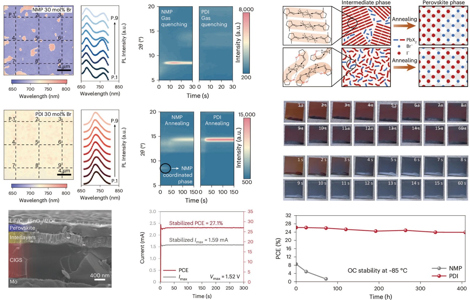
Crystallization Suppression of Mixed-Halide Intermediates for Perovskite/Cu(In,Ga)Se2 Tandem Solar Cells with Improved Efficiency

Authors: Manya Li, Linjing Jing, Hairen Tan

Flexible and lightweight photovoltaics are pivotal for renewable energy applications, and all-thin-film tandem solar cells combining metal-halide perovskites with copper indium gallium selenide (CIGS) offer a synergistic approach to exceed the Shockley-Queisser limit. However, fabricating high-quality wide-bandgap (WBG) perovskite films, especially via scalable blade-coating in ambient air, remains challenging due to uncontrollable crystallization kinetics, phase segregation, and moisture-induced defects. This work addresses these issues by introducing a crystallization suppression strategy that replaces the traditional solvent N-methyl-2-pyrrolidone (NMP) with 2-pyrrolidinone (PDI). In situ grazing-incidence X-ray diffraction (GIXRD) reveals that NMP-based films undergo a crystalline-to-crystalline transition via solvent-coordinated intermediates, leading to residual impurities and incomplete phase transformation. In contrast, PDI, through additional hydrogen bonding, suppresses pre-crystallization and maintains a homogeneous non-crystalline precursor state, enabling a rapid non-crystalline-to-crystalline transition with lower energy barriers. This results in uniform, pinhole-free films with enhanced carrier mobility, longer carrier lifetimes, and reduced trap densities. Single-junction perovskite solar cells fabricated with PDI achieve significantly improved efficiency, demonstrating the effectiveness of this approach for high-performance perovskite/CIGS tandem solar cells.

Crystallization Suppression of Mixed-Halide Intermediates for Perovskite/Cu(In,Ga)Se2 Tandem Solar Cells with Improved Efficiency
Graphical Abstract
Original ResearchVol. 32, Issue 2 • pp. 100-112DOI: 10.1088/1674-4926/26020007Jan 15, 2026

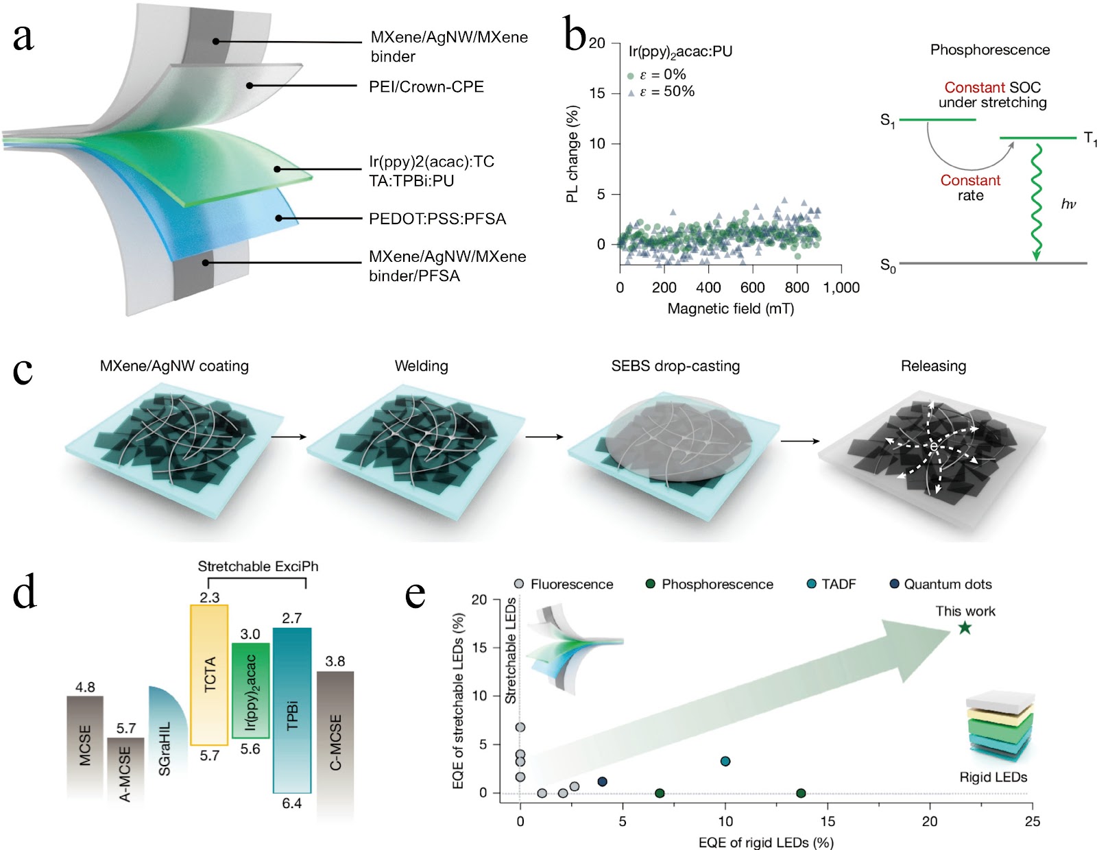
Exciplex-Enabled Fully Stretchable OLEDs Achieve a Record External Quantum Efficiency of 17%

Authors: Meng Wang, Liang Li

Organic light-emitting diodes (OLEDs) are promising candidates for on-skin applications due to their intrinsic stretchability. However, the external quantum efficiency (EQE) of stretchable OLEDs has long been limited to approximately 10%, stemming from the incorporation of insulating elastomer matrices that hinder exciton energy transfer and charge transport, and from conventional stretchable electrodes with insufficient electrical properties and poor interfacial contact. In a recent breakthrough published in Nature (2026), Gogotsi and Lee reported an exciplex-enabled strategy that overcomes these limitations. By integrating a stretchable exciplex-assisted phosphorescent emitting layer, triplet harvesting is significantly enhanced through an elastomer-tolerant triplet-recycling mechanism. Furthermore, they employ work-function-tunable MXene-contact stretchable electrodes (MCSEs) that provide two-dimensional electrical contact for efficient charge injection. Combining these advances, they achieve an unprecedented EQE of 17% in fully stretchable OLEDs while maintaining excellent mechanical stability. The spin-flip process, which converts non-radiative triplets into radiative singlets, is critical yet challenging in stretchable OLEDs because the necessary spin-orbit coupling (SOC) is sensitive to variations in intermolecular distance under strain. The authors utilize the phosphorescent emitter bis(2-phenylpyridine) (Ir(ppy)2acac), whose heavy-metal iridium center provides strong SOC, enabling nearly complete intersystem crossing and triplet utilization. The study demonstrates that the intrinsic SOC of Ir(ppy)2acac remains stable under 50% tensile strain, preserving both spin-mixing rates and photoluminescence stability. To prevent aggregation-induced quenching and enable efficient energy transfer within a soft matrix, the authors develop a stretchable exciplex-assisted phosphorescent (ExciPh) layer using TCTA and TPBi to form an exciplex cohost, while a thermoplastic polyurethane (PU) elastomer provides mechanical stretchability. This system enables triplet excitons to undergo reverse intersystem crossing (RISC) within a charge-transfer state, followed by long-range Förster resonance energy transfer (FRET) to the phosphorescent dopant. The fabricated OLED demonstrates an EQE of 21.7%, validating the effectiveness of this approach. Beyond the emissive layer, the researchers develop MXene-conductive stretchable electrodes (MCSEs) by integrating a two-dimensional MXene interlayer with silver nanowire (AgNW) networks, achieving a sheet resistance of ~30 Ω/sq with over 85% transmittance at 550 nm and a widely tunable work function (3.79–5.71 eV). They also introduce a stretchable gradient hole injection layer (SGraHIL) that suppresses exciton quenching at the interface while maintaining excellent stretchability. By integrating the SGraHIL, the ExciPh emitting layer, and MCSE electrodes, the authors fabricate fully stretchable OLEDs that achieve an unprecedented EQE of 17%, retaining 83% of initial efficiency after 100 cycles of 20% cyclic strain. This work represents a significant advance in intrinsically stretchable optoelectronics, offering a scalable route toward highly conductive, work-function-tunable contacts and influencing broader fields such as stretchable sensors and soft photonic systems.

Exciplex-Enabled Fully Stretchable OLEDs Achieve a Record External Quantum Efficiency of 17%
Graphical Abstract
Original ResearchVol. 32, Issue 2 • pp. 100-112DOI: 10.1088/1674-4926/26020017Jan 15, 2026

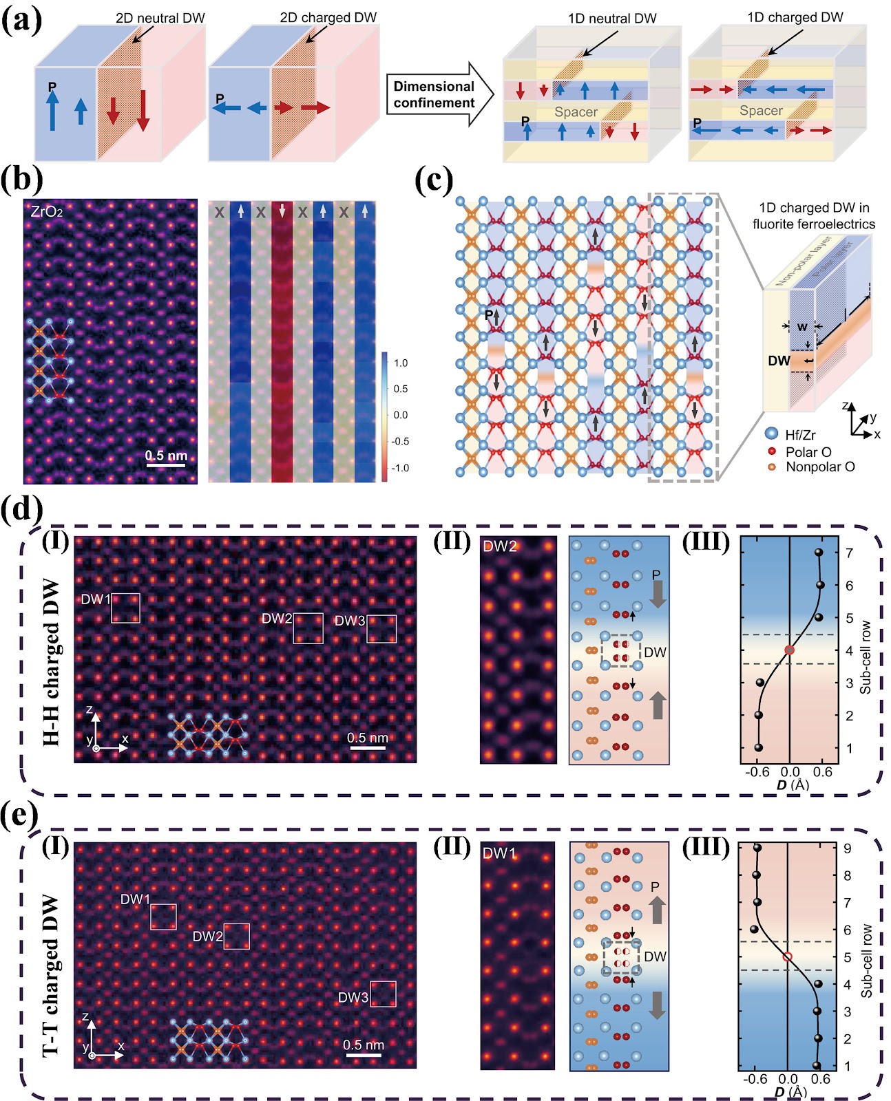
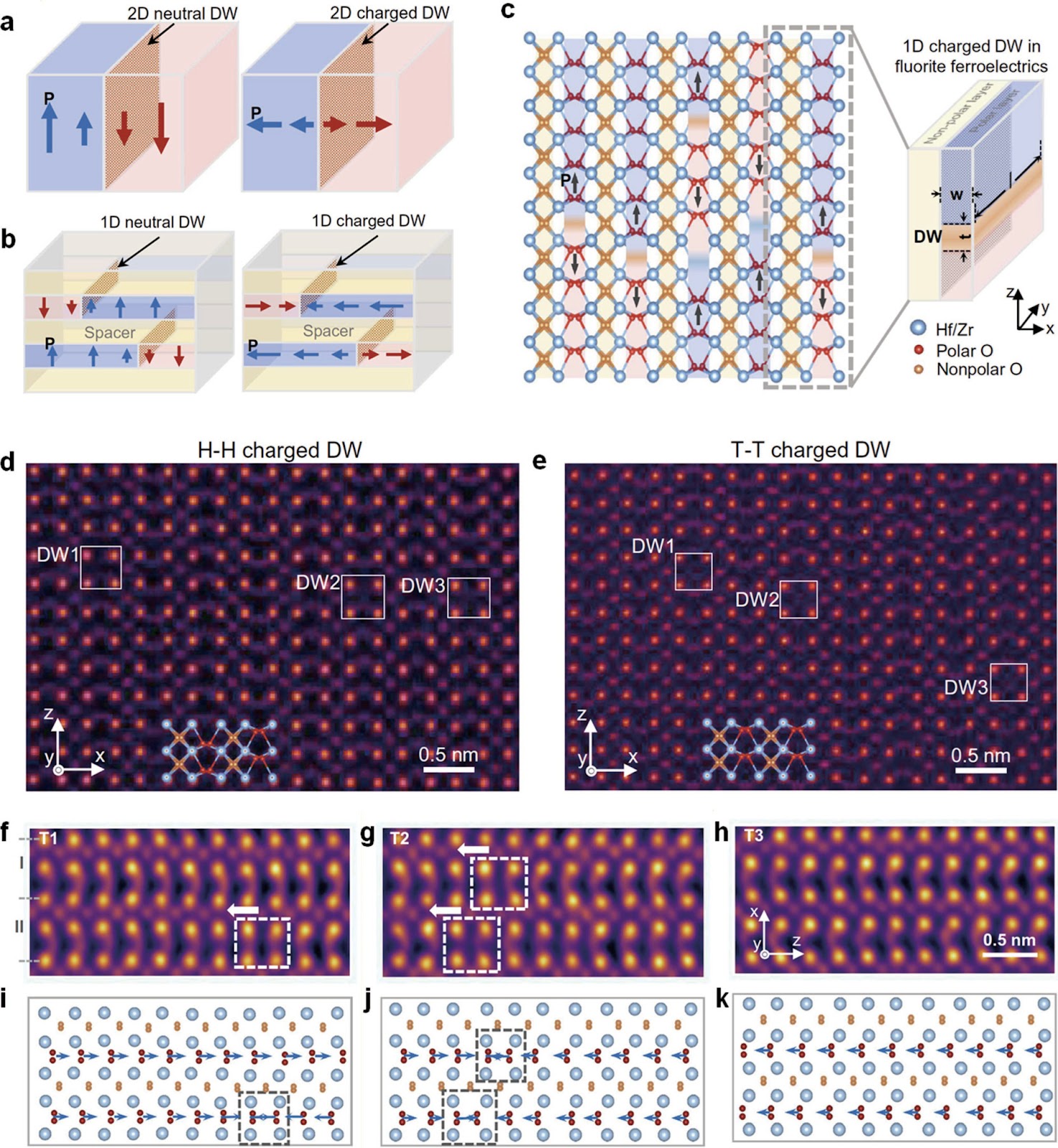
One-dimensional domain walls: A new dimension for ferroelectric nanoelectronics

Authors: Zepeng Li, Wenjing Yue, Yang Li

Topological structures in ferroelectric materials, such as vortices, skyrmions, and merons, have attracted significant attention due to their emergent physical properties distinct from the bulk parent phase. Among these, ferroelectric domain walls (DWs) have long been considered potential active elements for next-generation electronic devices, leading to the paradigm of "domain wall nanoelectronics." However, conventional perovskite ferroelectrics exhibit two-dimensional (2D) domain walls, and charged domain walls (CDWs) suffer from structural broadening due to electronic screening, limiting miniaturization. Recently, a research team led by Chen Ge, Kui-juan Jin, and Qinghua Zhang from the Institute of Physics, Chinese Academy of Sciences, reported the groundbreaking observation of one-dimensional (1D) CDWs in fluorite-structured ferroelectric ZrO2, achieving atomic-scale confinement. Using multislice electron ptychography, they visualized head-to-head and tail-to-tail CDWs with atomic-scale width and thickness (~2.55 Å and ~2.7 Å), equivalent to a single subcell unit. The stability of these atomically thin walls is attributed to a distinct ionic screening mechanism: self-balanced oxygen nonstoichiometry, where H–H walls accumulate excess oxygen ions and T–T walls harbor oxygen vacancies. Furthermore, in situ electric-field experiments demonstrated dynamic manipulation of these 1D structures, revealing a coupling between polarization switching and oxygen ion transport. This discovery breaks the inherent physical limitations of perovskite ferroelectrics and opens new avenues for high-density ferroelectric nanoelectronics.

One-dimensional domain walls: A new dimension for ferroelectric nanoelectronics
Graphical Abstract
Original ResearchVol. 32, Issue 2 • pp. 100-112DOI: 10.1088/1674-4926/26020057Jan 15, 2026

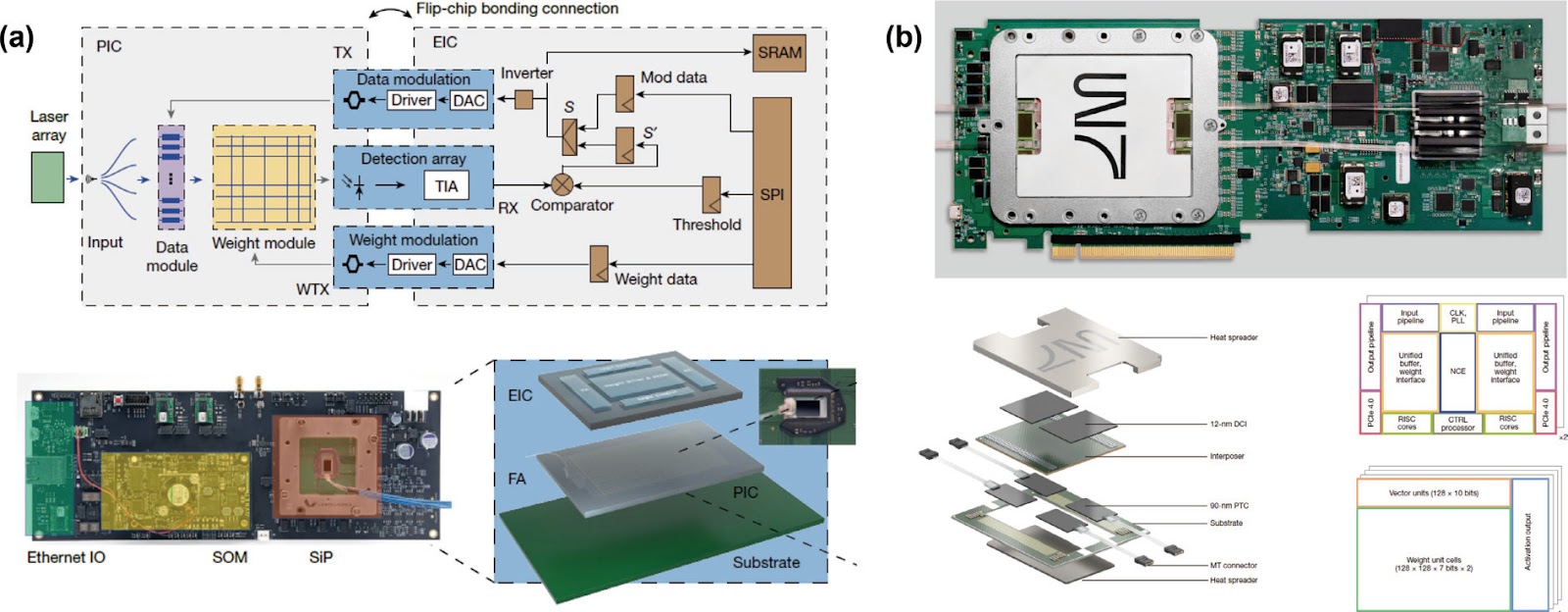
Large-scale integrated photonic accelerators for ultralow-latency and universal AI computing

Authors: Xiangyan Meng, Junshen Li, Kangwei Fei, Yu Wang, Wei Li, Nuannuan Shi, Ming Li

Integrated silicon photonics has emerged as a transformative technology for post-Moore's law computing, offering intrinsic advantages of high bandwidth, ultralow latency, and low energy consumption that far exceed traditional electronic computing architectures. As artificial intelligence (AI) models continue to grow in complexity and scale, the demand for high-speed, energy-efficient computing has spurred intensive research into photonic computing as a promising alternative to electronic accelerators. Matrix multiply-accumulate (MAC) operations, the core of deep learning and combinatorial optimization algorithms, are particularly amenable to photonic implementation, as light enables parallel multiplication and accumulation with minimal data movement. However, the practical application of photonic computing has long been hindered by critical challenges including large-scale integration of photonic components, electro-optical co-packaging, guaranteed computation accuracy of analog photonic systems, and compatibility with mainstream AI models and algorithms. Recently, two groundbreaking studies published back-to-back in Nature have achieved pivotal breakthroughs in addressing these bottlenecks, demonstrating large-scale integrated photonic accelerators with ultralow latency for combinatorial optimization and universal AI computing capabilities for state-of-the-art neural networks. The two works represent the most advanced level of photonic computing hardware implementation to date, validating the feasibility of photonic accelerators as a competitive alternative to electronic AI chips and marking a critical step toward the commercialization of integrated photonic computing technology.

Large-scale integrated photonic accelerators for ultralow-latency and universal AI computing
Graphical Abstract
Original ResearchVol. 32, Issue 2 • pp. 100-112DOI: 10.1088/1674-4926/26020013Jan 15, 2026

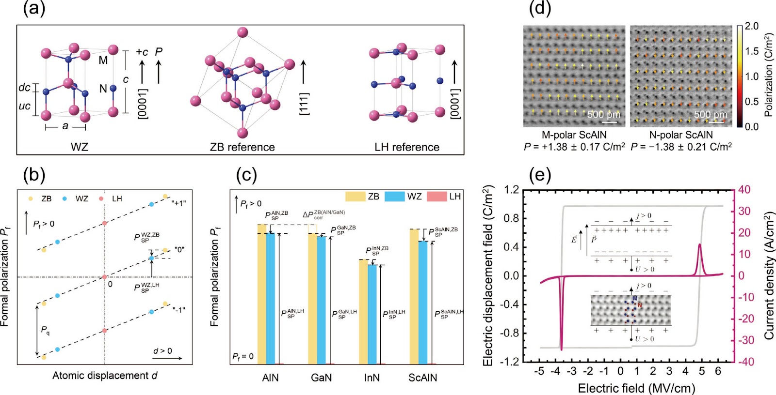
Re-benchmarking Polarization in Wurtzite Nitride Semiconductors

Authors: Ping Wang, Haotian Ye, Rui Wang, Tao Wang, Fang Liu, Zhaoying Chen, Ding Wang, Bo Shen, Xinqiang Wang

Polarization is a defining lever of wurtzite (WZ) III-nitrides. It enables two-dimensional electron and hole gases (2DEG and 2DHG), supports polarization doping, and provides electrostatic control for GaN-based power and radio-frequency (RF) electronics and nitride optoelectronics. Recent advances, especially the emergence of ferroelectric nitrides, have pushed polarization to unprecedented magnitudes and elevated it from a static material constant to an engineering knob. However, the field has long been limited by an uncomfortable reality: the magnitude and orientation of polarization, and its mapping to crystal polarity, have not always been expressed in a self-consistent, experimentally benchmarked language. This mini-review highlights recent progress that rethinks and unifies polarization in wurtzite III-nitride semiconductors. It also discusses how experimental re-benchmarking of giant polarization is reshaping our understanding of nitride polarization and unlocking more predictive polarization engineering for heterostructures and devices.

Re-benchmarking Polarization in Wurtzite Nitride Semiconductors
Graphical Abstract
Original ResearchVol. 32, Issue 2 • pp. 100-112DOI: 10.1088/1674-4926/26020026Jan 15, 2026

One-dimensional charged domain walls in fluorite ferroelectrics

Authors: Jiajia Chen, Haoji Qian, Xiaoxi Li, Yan Liu, Chengji Jin, Genquan Han

Ferroelectric domain walls are conventionally regarded as two-dimensional (2D) interfacial objects that separate regions of different polarization within a crystal. This picture has guided decades of research into polarization switching, domain evolution, and ferroic functionality. In most ferroelectrics, electrostatic considerations strongly favor head-to-tail (H–T) polarization configurations, which minimize bound charge and reduce electrostatic energy. By contrast, charged domain walls (CDWs) carry positive or negative bound polarization charge and form where polarization vectors arrange head-to-head (H–H) or tail-to-tail (T–T), generally considered energetically unfavorable. When such charged walls do occur, they are typically stabilized only as extended 2D structures through a combination of electronic screening, defect accumulation, and lattice relaxation. Despite these energetic constraints, CDWs have attracted growing interest over the past decade because of their emergent functional properties, including enhanced electrical conductivity, strong electromechanical coupling, and reconfigurable electronic behavior localized at charged walls, motivating the broader concept of domain-wall nanoelectronics. Nevertheless, ferroelectric domain walls have almost universally been treated as quasi-2D objects. Further reduction of their dimensionality has long been assumed to be impractical, particularly for charged walls, because confining bound polarization charge to lower dimensions would dramatically increase electrostatic energy. Against this backdrop, Zhong et al. reported the direct observation of one-dimensional (1D) CDWs confined within individual polar layers of ferroelectric ZrO2 (Science (2026)). Using atomic-resolution electron microscopy combined with in situ electric-field manipulation, they demonstrated that both H–H and T–T CDWs can exist as atomic-scale line defects rather than extended 2D interfaces, with their bound polarization charge stabilized through a self-balancing oxygen compensation mechanism. The discovery represents an extreme limit of ferroelectric domain-wall confinement and introduces a fundamentally new class of polar topological objects that occupy an intermediate conceptual regime between conventional domain walls and line defects.

One-dimensional charged domain walls in fluorite ferroelectrics
Graphical Abstract
Original ResearchVol. 32, Issue 3 • pp. 100-112DOI: 10.1088/1674-4926/26030014Jan 15, 2026

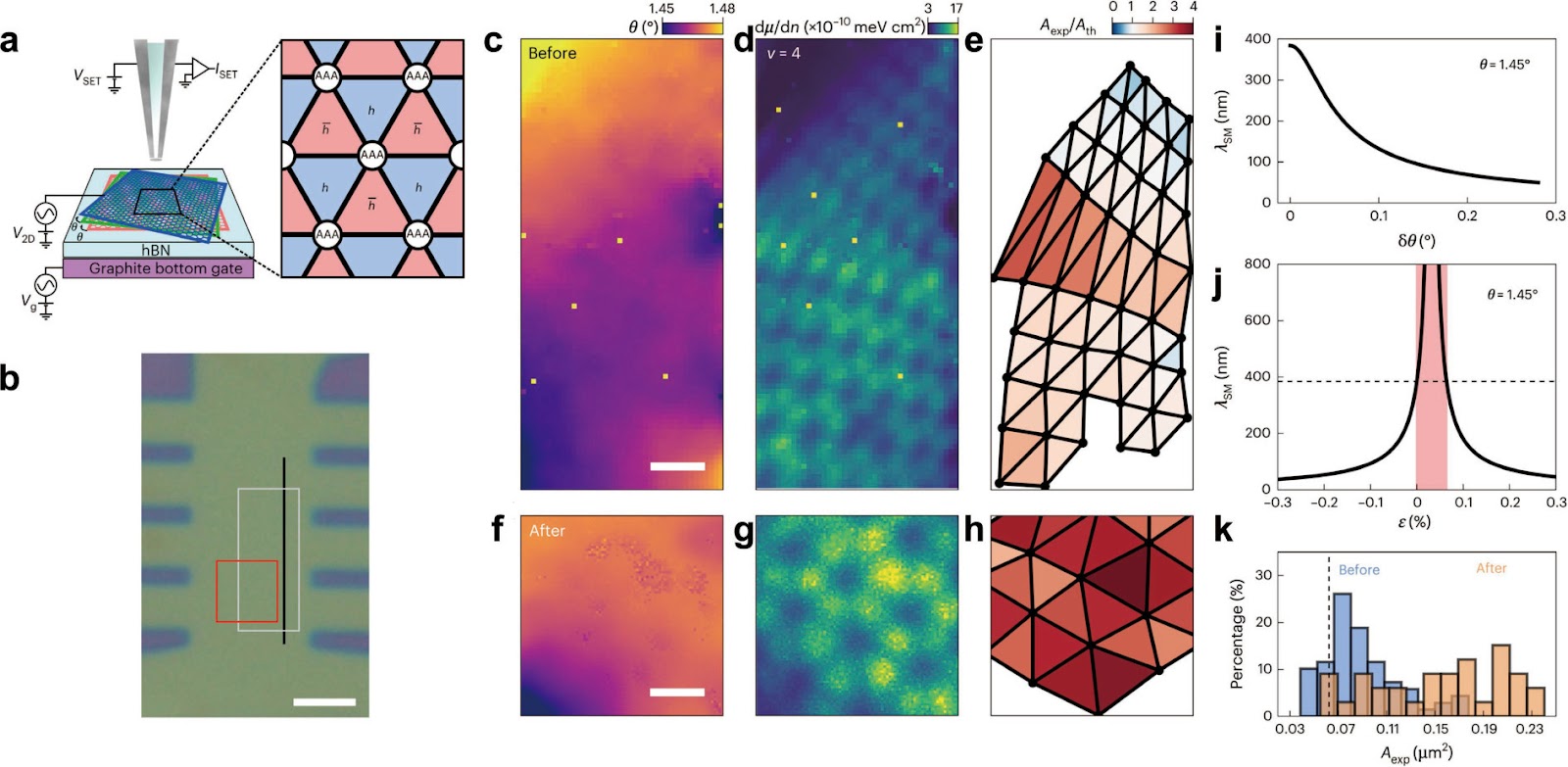
Supermoiré Domains in Helical Trilayer Graphene

Authors: Wen-Jun Wang, Ping-Heng Tan, Xin Zhang

Helical trilayer graphene (HTG), composed of three graphene layers with equal twist angles in the same rotational sense, has emerged as a rich platform for studying moiré physics. Theoretical predictions suggest that lattice relaxation in HTG leads to the formation of triangular domains with uniform moiré wavelength, arranged on a larger supermoiré length scale, with adjacent domains carrying opposite Chern numbers and hosting topological boundary modes. In a recent study, Hoke and colleagues directly imaged this supermoiré landscape using a scanning single-electron transistor (SET) probe sensitive to local electronic compressibility. Their measurements revealed a periodic modulation with a length scale of several hundred nanometers, far exceeding the moiré wavelength, consistent with theoretical predictions. The spatial maps showed a triangular lattice of domain centers and a honeycomb network of AAA-stacking regions, separated by domain walls with reduced compressibility. Notably, the observed domain areas deviated from ideal expectations, indicating the presence of heterostrain. Modeling showed that biaxial strain applied to the middle layer can substantially enhance the supermoiré wavelength, with a divergence at a critical strain. After thermal cycling, the device exhibited larger and more isotropic supermoiré domains while the local twist angle remained unchanged, demonstrating that strain can be used to engineer the supermoiré network without perturbing local moiré physics. These findings underscore that lattice relaxation and strain are powerful tuning parameters in twistronics, with implications for engineering topological and correlated phases in twisted multilayers.

Supermoiré Domains in Helical Trilayer Graphene
Graphical Abstract
Original ResearchVol. 32, Issue 2 • pp. 100-112DOI: 10.1088/1674-4926/26020023Jan 15, 2026

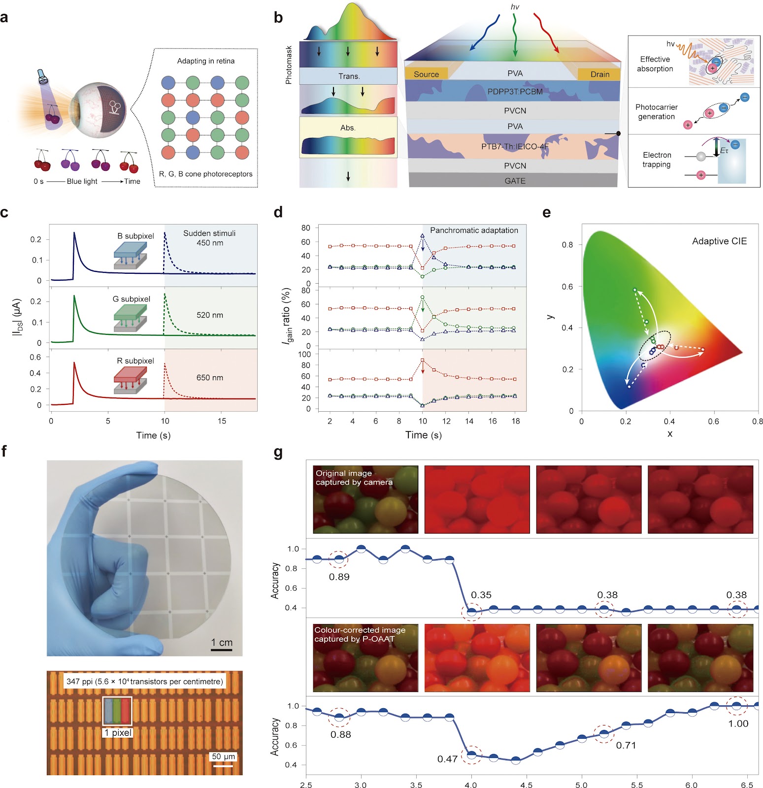
Three-Panchromatic Organic Self-Adaptive Transistors for In-Pixel Color Correction

Authors: Yuan Tan, Wei Deng, Xiujuan Zhang, Jiansheng Jie

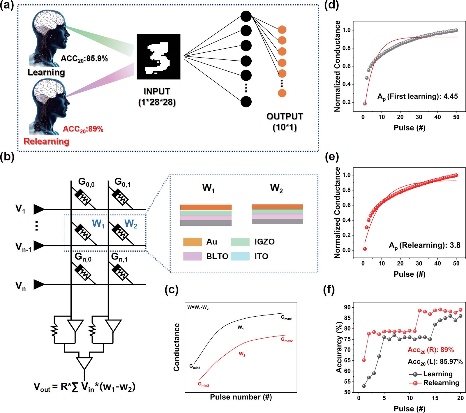
Machine vision systems face a fundamental challenge of illumination-dependent color shift, which conventional post-capture white-balance correction methods address at the cost of computational overhead and latency. Inspired by the human retina's chromatic adaptation, we propose a three-panchromatic organic self-adaptive transistor (OAAT) that embeds color correction directly at the pixel level. The device integrates a dual-layer complementary bulk heterojunction (BHJ) into an organic transistor architecture: a PTB7-Th:IEICO-4F blend serves as the adaptive photoresponse layer with broad-spectrum absorption and wavelength-insensitive trap activation energy that decreases with light intensity, while a PDPP3T:PCBM layer provides spectrally compensatory sensing. This design enables rapid, stable, and intensity-dependent photoadaptation, with an active adaptation index exceeding 150 for red, green, and blue stimuli. Under spectrally biased illumination, the device's responses follow von Kries coefficients and converge to a white-like chromatic state within seconds, demonstrating true chromatic adaptation. Wafer-scale fabrication achieved a 96.1% yield across 256 transistors, with pixel density of 347 ppi and over one million pixels integrated on a four-inch sapphire substrate. In a hybrid artificial visual system combining the OAAT array with a lightweight CNN, in-sensor correction restored classification accuracy for 'frog' in CIFAR-10 from 59.1% to 96.3% under blue-light interference, and outperformed conventional RGB cameras in real-world non-uniform lighting. This work presents a scalable, hardware-based solution for in-pixel color correction, promising for energy-efficient and real-time machine vision.

Three-Panchromatic Organic Self-Adaptive Transistors for In-Pixel Color Correction
Graphical Abstract
Original ResearchVol. 32, Issue 2 • pp. 100-112DOI: 10.1088/1674-4926/26020002Jan 15, 2026

Mitigating phosphonic acid-perovskite interfacial degradation via molecular engineering for ultra-stable solar cells

Authors: LI Xu, GUO Yuxiao, LUO Xin, YAN Haoyuan, XU Bo

Metal halide perovskite solar cells (PSCs) are revolutionizing next-generation photovoltaics by combining high efficiency with low-cost solution processing and flexible compatibility. Certified efficiencies now surpass 27%, nearing the theoretical limit for single-junction cells and highlighting their strong potential for commercialization. In contrast to traditional silicon cells, which require high-temperature processing and rigid substrates, PSCs can be fabricated near room temperature using earth-abundant materials, significantly lowering energy consumption and production costs. However, their commercialization is hindered by a fundamental challenge: insufficient long-term operational stability. PSCs must endure harsh real-world conditions, including elevated temperatures (≥85 °C) and full-spectrum illumination. Meeting the International Electrotechnical Commission (IEC) standard of ≥25 years of service life remains an unresolved critical hurdle for SAM-based PSCs. The hole-transport layer (HTL) plays a decisive role in both the efficiency and long-term stability of PSCs, responsible for efficiently extracting photogenerated holes from the perovskite layer to the transparent conductive oxide electrode. Inadequate extraction leads to severe interfacial charge recombination and significant efficiency losses. Among various HTL materials, phosphonic acid-based self-assembled monolayers (PA-SAMs) have become the material of choice for inverted-structure PSCs, owing to their molecular-scale precision, ultrathin film formation, and superior energy-level alignment—properties that effectively suppress non-radiative recombination and enhance initial device performance. Nevertheless, their practical application is severely limited by an inherent flaw: PA-SAMs primarily anchor to ITO surfaces via weak hydrogen bonds, which dissociate under photothermal stress. This triggers molecular desorption and migration into the perovskite layer, inducing degradation and eventual performance decline. To tackle this persistent issue, Fei et al. report a transformative molecular engineering strategy that unlocks ultra-stable PSCs (Science 2026, https://doi.org/10.1126/science.adz7969). The team designed a triphenylamine-based phosphonic acid (1PA-TPD) with robust covalent anchoring to ITO substrates and optimized a mixed SAM system (60 wt% 1PA-TPD + 40 wt% EtCz3EPA), successfully suppressing interfacial reactivity between PA-SAMs and perovskites. This multifunctional strategy integrates strong substrate binding, interfacial reaction inhibition, crystallinity enhancement, and defect passivation.

Mitigating phosphonic acid-perovskite interfacial degradation via molecular engineering for ultra-stable solar cells
Graphical Abstract
Original ResearchVol. 32, Issue 2 • pp. 100-112DOI: 10.1088/1674-4926/26020058Jan 15, 2026

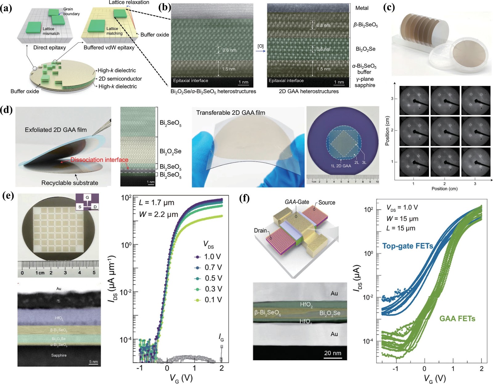
A Transferable Route to Two-Dimensional Gate-All-Around Electronics

Authors: Jian Wang, Ruiqin Wu, Jianfeng Jiang

The relentless drive for miniaturization in microelectronics, guided by Moore's Law, is approaching a critical inflection point. Silicon-based transistors are confronting fundamental physical limits at the atomic scale, where issues of power leakage and degraded electrostatic control become increasingly severe. To sustain performance scaling, the semiconductor industry is transitioning to gate-all-around (GAA) nanosheet architectures for sub-2-nanometer technology nodes. However, integrating atomically thin two-dimensional (2D) semiconductors as channel materials within GAA structures offers a revolutionary path, promising superior electrostatic control and lower power consumption. The grand challenge has been the absence of a scalable, industry-compatible method to synthesize high-quality, uniform 2D semiconductor channels seamlessly encapsulated by high-k gate dielectrics in a GAA configuration. A groundbreaking study by Peng et al. reports the wafer-scale, uniform synthesis of single-crystalline 2D high-k dielectric/semiconductor/high-k dielectric GAA heterostructures via an innovative buffered van der Waals epitaxy technique. The core innovation lies in pre-depositing a high-k van der Waals buffer oxide (α-Bi2SeO5) on an r-plane sapphire substrate, which mitigates lattice mismatch and enables epitaxial growth of uniform Bi2O2Se films. Controlled oxidation transforms the top layer into β-Bi2SeO5, forming a sandwich-like GAA heterostructure with atomically sharp interfaces. The intrinsic transferability of these stacks allows clean exfoliation and transfer onto arbitrary substrates, leaving the sapphire wafer reusable. Field-effect transistors fabricated from these heterostructures exhibit outstanding electrical characteristics: on/off ratios exceeding 10^6 and carrier mobility up to 227 cm²·V⁻¹·s⁻¹. True GAAFETs using both top and bottom gates show improved subthreshold swing and higher on/off ratios, demonstrating superior gate controllability. This work represents a foundational platform technology addressing critical integration challenges for 2D semiconductors, bridging laboratory exploration and foundry-level manufacturing, and enabling monolithic 3D integration for future electronics.

A Transferable Route to Two-Dimensional Gate-All-Around Electronics
Graphical Abstract
Original ResearchVol. 32, Issue 2 • pp. 100-112DOI: 10.1088/1674-4926/26020030Jan 15, 2026

Stabilizing Perovskite Fabrication in Ambient Air

Authors: GONG Ruihao, YAN Buyi, LAN Dongchen

Perovskite-based solar cells have advanced rapidly due to their high efficiency potential, low-cost processing, and flexible fabrication routes. While silicon solar cells remain the dominant commercial technology, combining perovskites with silicon in tandem architectures offers a clear pathway to exceed the efficiency limits of single-junction devices. By pairing perovskite's tunable absorption with silicon's proven performance, perovskite–silicon tandem solar cells open new opportunities for high-efficiency photovoltaics. Yet translating these advances from laboratory demonstrations to scalable manufacturing remains a major challenge. A central obstacle lies in fabricating high-quality perovskite films under ambient conditions. Moisture in air directly interferes with perovskite crystallization, leading to disordered crystal growth, surface degradation, and the accumulation of non-ideal secondary phases. Although thermal annealing is often used to improve crystallinity, the combined effects of heat and humidity can instead accelerate irreversible degradation when processing in air. Together, these factors make crystallization control under ambient conditions particularly difficult, underscoring the need for new strategies that can stabilize film formation without relying on tightly controlled environments. Previous studies have explored several approaches to optimize perovskite film fabrication in ambient air, such as solvent engineering and longitudinal homogeneous intermediates in hybrid sequential deposition, as well as techniques like the P1.5 process that introduce a diffusion barrier layer. However, challenges persist, particularly in achieving the same performance as films fabricated in controlled environments. Now, writing in Joule, Tan et al. tackle this challenge with a novel approach that intervenes in the wet-film stage to stabilize the crystallization process. Instead of relying on environmental controls to eliminate moisture, the authors introduce an additive, n-butylammonium thiocyanate (nBASCN), to regulate crystallization dynamics. Implemented as part of the hybrid sequential deposition process, this wet-film intervention modifies the crystallization pathway, preventing premature nucleation and promoting uniform growth. The key innovation lies in the use of nBASCN to decouple diffusion from crystallization, enabling uniform crystallization and improving film quality under ambient conditions. This intervention not only improves film quality but also enhances device performance, with nBASCN-treated devices achieving higher power conversion efficiency (PCE) compared to untreated controls. Beyond improving single-junction perovskite solar cells, this approach is also effective for tandem solar cells, demonstrating the strategy's applicability to more complex multi-junction devices. This marks a crucial step toward achieving scalable, high-efficiency tandem solar cells.

Stabilizing Perovskite Fabrication in Ambient Air
Graphical Abstract
Original ResearchVol. 32, Issue 2 • pp. 100-112DOI: 10.1088/1674-4926/26020044Jan 15, 2026

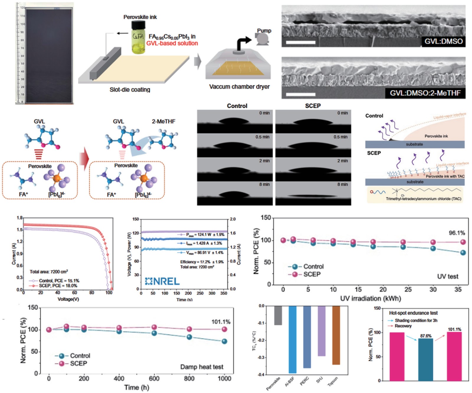
Improved Solvent Systems for the Commercialization of Perovskite Photovoltaic Modules

Authors: Zhaoyang Chu, Xiaotian Hu, Yiwang Chen

Perovskite solar cells (PSCs) are widely recognized as a transformative technology for next-generation photovoltaics, given their exceptional promise for achieving high power conversion efficiencies (PCE), utilizing low-cost raw materials, and enabling versatile fabrication routes. However, commercialization efforts continue to face considerable obstacles, such as the dependence on toxic solvents, inadequate uniformity in large-area film deposition, and limited operational durability. Conventional perovskite inks commonly rely on highly toxic, high-boiling-point aprotic polar solvents, including N,N-dimethylformamide (DMF) and N-methyl-2-pyrrolidone (NMP). These solvents present serious environmental and health hazards while also impeding processing speeds and perovskite film quality in scalable high-throughput manufacturing, such as roll-to-roll slot-die coating, owing to their slow evaporation kinetics. Furthermore, residual solvent and heterogeneous crystallization tend to introduce a high density of defects in perovskite films, which undermines the long-term stability and reliability of the resulting perovskite photovoltaic modules (PPM) and hinders compliance with the rigorous standards required for commercial deployment. Thus, the establishment of an eco-friendly and efficient solvent system is essential for enabling the widespread adoption of perovskite technology in the mainstream photovoltaic market. In this context, Wang et al. devised an eco-friendly ink formulation utilizing green solvents (γ-valerolactone (GVL), dimethylsulfoxide (DMSO) and 2-methyltetrahydrofuran (2-MeTHF)), and integrated it with a solvent-constrained edge-protection (SCEP) strategy. This approach enhanced the edge quality of perovskite films and lowered defect density under ambient conditions, thereby enabling the scalable production of high-performance PPM (Science, 2025, 390, 1021-1028). These approaches enabled the production of 7200-square-centimeter PPM that achieved a certified stabilized efficiency of 17.2% by NREL. In addition, the scalable module passed all IEC 61215 reliability standards as certified by TÜV Rheinland. This work has realized a PPM with a certified stabilized efficiency of 17.2% over an area of 7200 cm2. The adoption of green solvents not only addresses environmental and regulatory concerns, but also owing to their lower boiling point and the optimized process flow, which reduces energy consumption during production. Combined with slot-die coating technology, which is well-suited for large-scale roll-to-roll manufacturing, the proposed solution demonstrates considerable potential for achieving highly competitive levelized cost of electricity in the future, thereby accelerating the commercialization of perovskite photovoltaics.

Improved Solvent Systems for the Commercialization of Perovskite Photovoltaic Modules
Graphical Abstract
Original ResearchVol. 32, Issue 4 • pp. 100-112DOI: 10.1088/1674-4926/26041001Jan 15, 2026

Preface to Focus Topic on Integrated Circuits, Technologies and Applications (ICTA) 2025

Authors: Yan Lu, Sai-Weng Sin

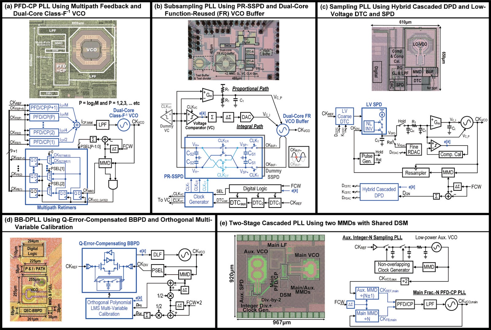
This Special Topic of the Journal of Semiconductors (JoS) features expanded versions of key articles presented at the 2025 IEEE International Conference on Integrated Circuits Technologies and Applications (ICTA), held in Macao, China, from October 22 to 24, 2025. IEEE ICTA is an IEEE flagship conference in the field of integrated circuits (IC) in China, providing a communication platform for sharing state-of-the-art techniques from experts in the field of ICs. Among the 146 papers presented at ICTA 2025, the Technical Program Committee and the Award Committee selected 3 high-quality articles for recommendation to the Special Topic of JoS, covering the technical fields of RF, medical neural interface, and vision sensing ICs. The first article, from Zhejiang University, introduces a fractional-N dual-path SPD/PFD PLL with a complementary digital-to-time converter (DTC) pair for DTC range reduction and INL cancellation, achieving 118 fs RMS jitter and -247.5 dB figure-of-merit in 7 nm FinFET. The second article, also from Zhejiang University, presents a battery-free neural interface with dual-overlapped on-chip antennas, enabling high-data-rate backscatter for 72-channel simultaneous recording, achieving 18 Mbps backscatter data rate in 65 nm CMOS. The third article, from the Southern University of Science and Technology, describes a cascadable stereo matching processor with a scalable semi-global matching algorithm, achieving speedups of up to 178x and 97x over CPU and Edge GPU platforms, respectively, with an energy efficiency of 7.9 pJ/pixel in 40-nm CMOS.

Preface to Focus Topic on Integrated Circuits, Technologies and Applications (ICTA) 2025
Graphical Abstract
Original ResearchVol. 32, Issue 2 • pp. 100-112DOI: 10.1088/1674-4926/26020015Jan 15, 2026

Ultrathin van der Waals Ferroelectric Oxides for Scalable Low-Power Memory

Authors: Xiaokun Qin, Bowen Zhong, Zheng Lou, Lili Wang

The continuous scaling of ferroelectric memories to below 5 nm has exacerbated challenges such as depolarization fields, interfacial charge trapping, and structural non-uniformity, which critically bottleneck the performance and consistency of ferroelectric field-effect transistors (FeFETs). Although van der Waals ferroelectrics offer a promising route to overcome interface-related issues and critical-thickness limits, the lack of wafer-scale, CMOS-compatible ultrathin ferroelectric materials with robust polarization and high dielectric constants has hindered practical deployment. In a recent study published in Science (2026), Peng and colleagues report a wafer-scale, ultrathin van der Waals ferroelectric oxide platform that addresses these challenges via a controlled oxidation strategy, transforming a two-dimensional semiconductor precursor into a layered ferroelectric oxide with atomically smooth and chemically coherent interfaces. This native-oxide approach enables robust and switchable polarization down to the monolayer limit, as demonstrated by domain writing and erasing. The platform supports monolithic integration of FeFET arrays over centimetre-scale areas, exhibiting consistent hysteresis windows and switching thresholds across hundreds of devices, with narrow distributions of on/off ratios and threshold voltages. Furthermore, the programmable coupling between ferroelectric polarization and semiconductor channels enables multi-level threshold voltage programmability and stable switching between logic states, positioning these devices as reconfigurable building blocks for low-power memory and computing-in-memory architectures. This work bridges the gap between atomic-scale ferroelectric physics and manufacturable device architectures, offering a scalable path for next-generation non-volatile memory.

Ultrathin van der Waals Ferroelectric Oxides for Scalable Low-Power Memory
Graphical Abstract
Original ResearchVol. 32, Issue 2 • pp. 100-112DOI: 10.1088/1674-4926/26020003Jan 15, 2026

Material Platforms for Solid-State Single-Photon Sources: Wide Bandgap Semiconductors

Authors: MENG Junhua, SHI Yiming, ZHANG Xingwang

Single-photon sources are essential components for scalable quantum information technologies, with applications spanning quantum communication, quantum key distribution, quantum computing, and quantum sensing. Color centers in the solid state, such as optically active point defects, are promising candidates for the next-generation single-photon sources. Their atom-like properties enable the emission of single photons with high efficiency, purity, and indistinguishability, while their solid-state nature allows for integration into scalable quantum photonic devices. Among these, color centers in wide-bandgap semiconductors stand out as exceptionally promising single-photon emitters (SPEs), owing to their stable room-temperature (or higher) operation and wide spectral tunability. Furthermore, their compatibility with mature semiconductor technology facilitates direct integration into practical optoelectronic systems. In recent years, such defect-based SPEs have been realized in a variety of wide-bandgap semiconductors, including diamond, silicon carbide (SiC), silicon nitride (Si3N4), gallium nitride (GaN), aluminum nitride (AlN), hexagonal boron nitride (h-BN), zinc oxide (ZnO), and beta-phase gallium oxide (β-Ga2O3). This mini-review summarizes recent progress in SPEs based on wide-bandgap semiconductors and discusses their potential for integrated quantum photonic circuits.

Material Platforms for Solid-State Single-Photon Sources: Wide Bandgap Semiconductors
Graphical Abstract
Original ResearchVol. 32, Issue 1 • pp. 100-112DOI: 10.1088/1674-4926/25010031Jan 15, 2025

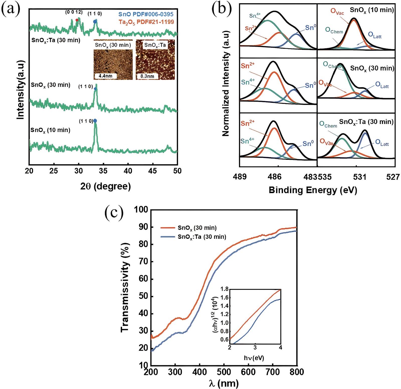
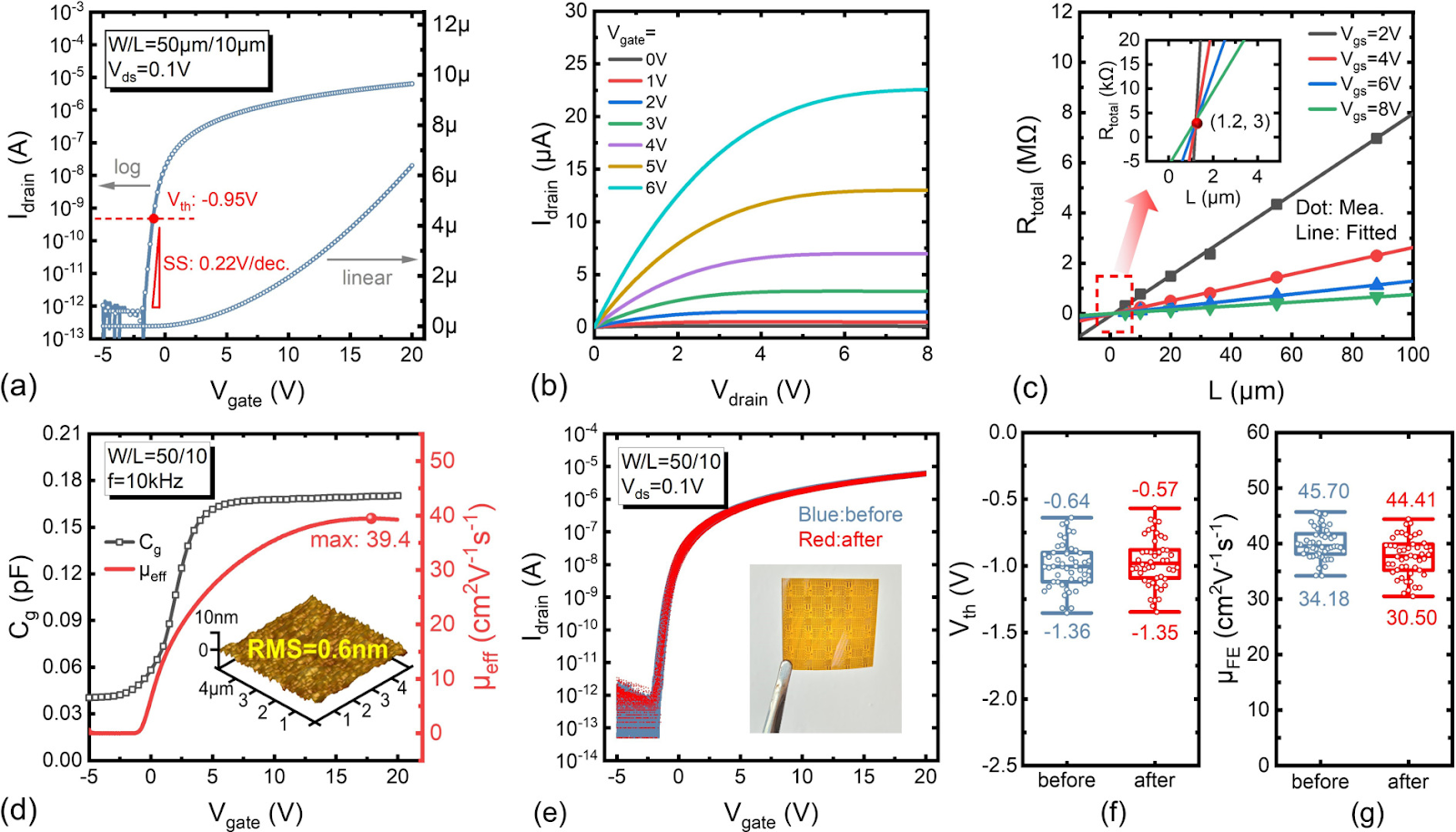
Improving electrical performance and fringe effect in p-type SnOx thin film transistors via Ta incorporation

Authors: Yu Song, Runtong Guo, Ruohao Hong, Rui He, Xuming Zou, Benjamin Iñiguez, Denis Flandre, Lei Liao, and Guoli Li

In this work, the incorporation of tantalum (Ta) into p-type metal-oxide (SnOx) semiconductor film is investigated to improve the electrical characteristics and suppress the fringe effect of thin film transistors (TFTs). The Ta-doped SnOx (SnOx:Ta) film is deposited by radio-frequency (RF) magnetron sputtering with a Sn:Ta (3 at.%) target and thermally annealed at 270 °C for 30 min. Here, we observe that the SnOx:Ta film presents increased crystallinity, reduced defect density (3.25 × 1012 cm−2·eV−1), and widened bandgap (1.98 eV), in comparison with the undoped SnOx film. As a result, the SnOx:Ta TFTs exhibit a lower off-state current (Ioff), an improved on/off current ratio (2.17 × 10⁴), a remarkably decreased subthreshold swing (SS) by 41%, and enhanced device stability. Additionally, by introducing Ta dopants, the fringe effect as well as the impact of channel width-to-length ratio (W/L) on electrical performances of the p-type oxide TFTs can be effectively suppressed. These results shall contribute to further exploration and development of p-type SnOx TFTs.

Improving electrical performance and fringe effect in p-type SnOx thin film transistors via Ta incorporation
Graphical Abstract
Original ResearchVol. 32, Issue 1 • pp. 100-112DOI: 10.1088/1674-4926/25010024Jan 15, 2025

AlGaN/GaN-based SBDs grown on silicon substrates with trenched n+-GaN cap layer and local passivation layer to improve BFOM and dynamic properties

Authors: Zhizhong Wang, Jingting He, Fuping Huang, Xuchen Gao, Kangkai Tian, Chunshuang Chu, Yonghui Zhang, Shuting Cai, Xiaojuan Sun, Dabing Li, Xiao Wei Sun, Zi-Hui Zhang

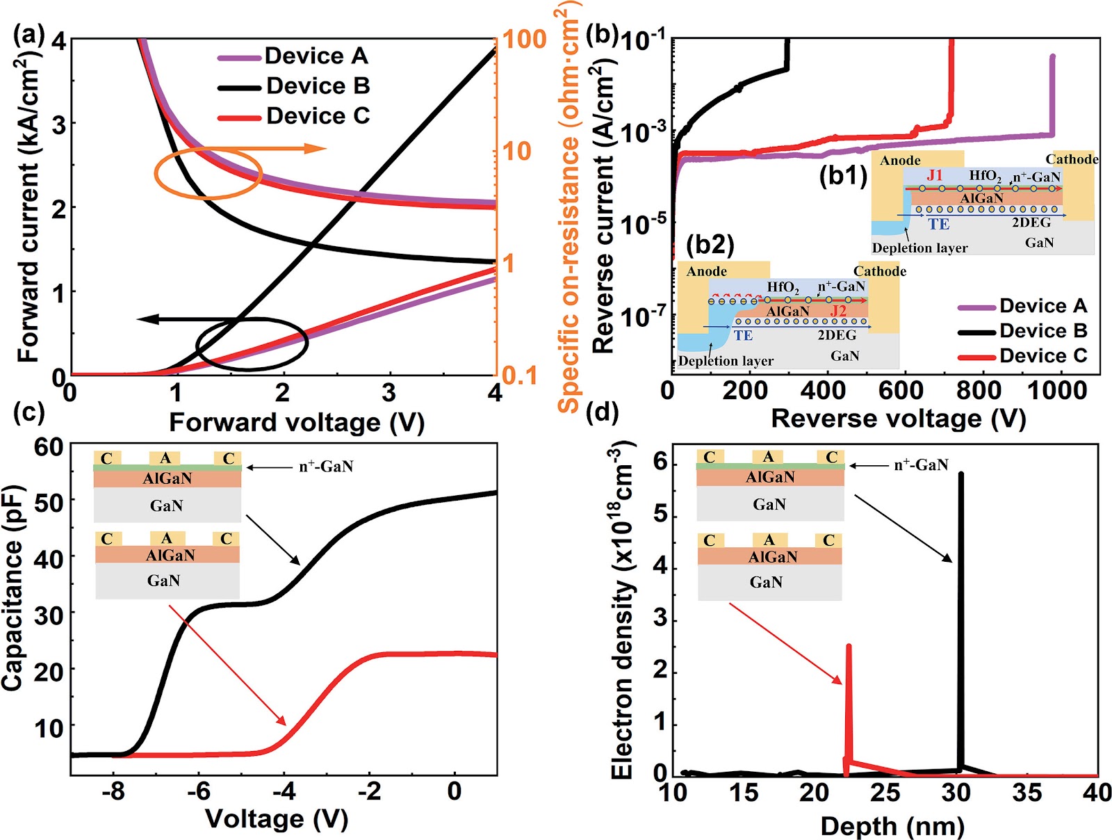
In this work, we design and fabricate AlGaN/GaN-based Schottky barrier diodes (SBDs) on a silicon substrate with a trenched n+-GaN cap layer. With the developed physical models, we find that the n+-GaN cap layer provides more electrons into the AlGaN/GaN channel, which is further confirmed experimentally. When compared with the reference device, this increases the two-dimensional electron gas (2DEG) density by two times and leads to a reduced specific ON-resistance (Ron,sp) of ~2.4 mΩ·cm2. We also adopt the trenched n+-GaN structure such that partial of the n+-GaN is removed by using dry etching process to eliminate the surface electrical conduction when the device is set in the off-state. To suppress the surface defects that are caused by the dry etching process, we also deposit Si3N4 layer prior to the deposition of field plate (FP), and we obtain a reduced leakage current of ~8 × 10⁻⁵ A·cm−2 and breakdown voltage (BV) of 876 V. The Baliga’s figure of merit (BFOM) for the proposed structure is increased to ~319 MW·cm−2. Our investigations also find that the pre-deposited Si3N4 layer helps suppress the electron capture and transport processes, which enables the reduced dynamic Ron,sp.

AlGaN/GaN-based SBDs grown on silicon substrates with trenched n+-GaN cap layer and local passivation layer to improve BFOM and dynamic properties
Graphical Abstract
Original ResearchVol. 32, Issue 1 • pp. 100-112DOI: 10.1088/1674-4926/25010026Jan 15, 2025

Reducing specific contact resistivity of V/Al/Ti/Au n-electrode on n-AlGaN with Al content over 80% for far-UVC LEDs

Authors: Jiale Peng, Ke Jiang, Shanli Zhang, Jianwei Ben, Kexi Liu, Ziyue Qin, Ruihua Chen, Chunyue Zhang, Shunpeng Lv, Xiaojuan Sun, Dabing Li

AlGaN-based LEDs with peak wavelength below 240 nm (far-UVC) pose no significant harm to human health, thus highlighting their broader application potential. While, there is a significant Schottky barrier between the n-electrode and Al-rich n-AlGaN, adversely impeding electron injection and resulting in considerable heat generation. Here, we fabricate V-based electrodes of V/Al/Ti/Au on n-AlGaN with Al content over 80% and investigate the relationship between the metal diffusion and contact properties during the high-temperature annealing process. Experiments reveal that decreasing V thickness in the electrode promotes the diffusion of Al towards the surface of n-AlGaN, which facilitates the formation of VN and thus the increase of local electron concentration, resulting in lower specific contact resistivity. Then, increasing the Al thickness inhibits the diffusion of Au to the n-AlGaN surface, suppressing the rise of Schottky barrier. Experimentally, an optimized n-electrode of V(10 nm)/Al(240 nm)/Ti(40 nm)/Au(50 nm) on n-Al0.81Ga0.19N is obtained, realizing an optimal specific contact resistivity of 7.30 × 10⁻⁴ Ω·cm2. Based on the optimal n-electrode preparation scheme for Al-rich n-AlGaN, the work voltage of a far-UVC LED with peak wavelength of 233.5 nm is effectively reduced.

Reducing specific contact resistivity of V/Al/Ti/Au n-electrode on n-AlGaN with Al content over 80% for far-UVC LEDs
Graphical Abstract
Original ResearchVol. 32, Issue 1 • pp. 100-112DOI: 10.1088/1674-4926/25010015Jan 15, 2025

Review on three-dimensional graphene: synthesis and joint photoelectric regulation in photodetectors

Authors: Bingkun Wang, Jinqiu Zhang, Huijuan Wu, Fanghao Zhu, Shanshui Lian, Genqiang Cao, Hui Ma, Xurui Hu, Li Zheng, Gang Wang

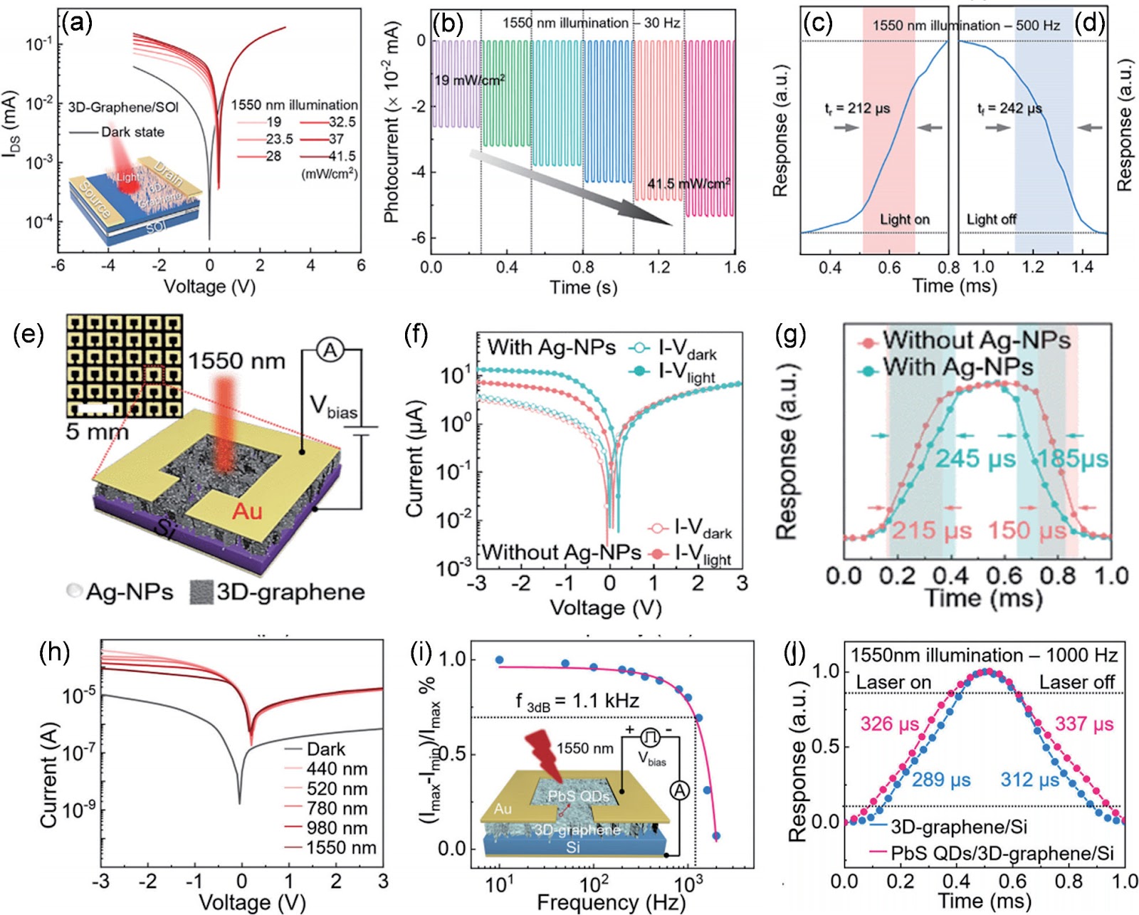
Graphene has garnered significant attention in photodetection due to its exceptional optical, electrical, mechanical, and thermal properties. However, the practical application of two-dimensional (2D) graphene in optoelectronic fields is limited by its weak light absorption (only 2.3%) and zero bandgap characteristics. Increasing light absorption is a critical scientific challenge for developing high-performance graphene-based photodetectors. Three-dimensional (3D) graphene comprises vertically grown stacked 2D-graphene layers and features a distinctive porous structure. Unlike 2D-graphene, 3D-graphene offers a larger specific surface area, improved electrochemical activity, and high chemical stability, making it a promising material for optoelectronic detection. Importantly, 3D-graphene has an optical microcavity structure that enhances light absorption through interaction with incoming light. This paper systematically reviews and analyzes the current research status and challenges of 3D-graphene-based photodetectors, aiming to explore feasible development paths for these devices and promote their industrial application.

Review on three-dimensional graphene: synthesis and joint photoelectric regulation in photodetectors
Graphical Abstract
Original ResearchVol. 32, Issue 1 • pp. 100-112DOI: 10.1088/1674-4926/25010027Jan 15, 2025

Investigating the doping performance of an ionic dopant for organic semiconductors and thermoelectric applications

Authors: Jing Guo, Yaru Feng, Jinjun Zhang, Jing Zhang, Ping-An Chen, Huan Wei, Xincan Qiu, Yu Liu, Jiangnan Xia, Huajie Chen, Yugang Bai, Lang Jiang, Yuanyuan Hu

Doping plays a pivotal role in enhancing the performance of organic semiconductors (OSCs) for advanced optoelectronic and thermoelectric applications. In this study, we systematically investigated the doping performance and applicability of the ionic dopant 4-isopropyl-4′-methyldiphenyliodonium tetrakis(penta-fluorophenyl-borate) (DPI-TPFB) as a p-dopant for OSCs. Using the p-type OSC PBBT-2T as a model system, we demonstrated that DPI-TPFB shows significant doping effect, as confirmed by ESR spectra, ultraviolet−visible−near-infrared (UV−vis−NIR) absorption, and work function analysis, and enhances the electronic conductivity of PBBT-2T films by over four orders of magnitude. Furthermore, DPI-TPFB exhibited broad doping applicability, effectively doping various p-type OSCs and even imparting p-type characteristics to the n-type OSC N2200, transforming its intrinsic n-type behavior into p-type. The application of DPI-TPFB-doped PBBT-2T films in organic thermoelectric devices (OTEs) was also explored, achieving a power factor of approximately 10 μW∙m−1∙K−2. These findings highlight the potential of DPI-TPFB as a versatile and efficient dopant for integration into organic optoelectronic and thermoelectric devices.

Investigating the doping performance of an ionic dopant for organic semiconductors and thermoelectric applications
Graphical Abstract
Original ResearchVol. 32, Issue 1 • pp. 100-112DOI: 10.1088/1674-4926/25010005Jan 15, 2025

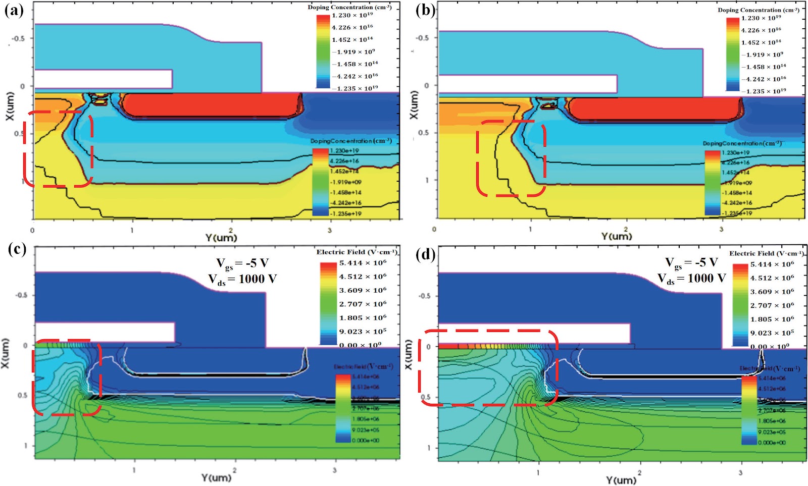
4H-SiC superjunction MOSFET with integrated high-K gate dielectric and split gate

Authors: Jiafei Yao, Zhengfei Yang, Yuxuan Dai, Ziwei Hu, Man Li, Kemeng Yang, Jing Chen, Maolin Zhang, Jun Zhang, Yufeng Guo

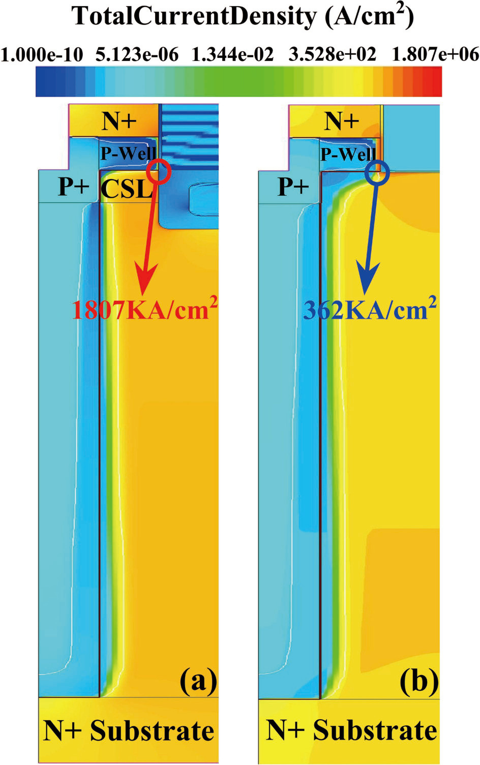
A 4H-SiC superjunction (SJ) MOSFET (SJMOS) with integrated high-K gate dielectric and split gate (HKSG-SJMOS) is proposed in this paper. The key features of HKSG-SJMOS involve the utilization of high-K (HK) dielectric as the gate dielectric, which surrounds the source-connected split gate (SG) and metal gate. The high-K gate dielectric optimizes the electric field distribution within the drift region, creating a low-resistance conductive channel. This enhancement leads to an increase in the breakdown voltage (BV) and a reduction in the specific on resistance (Ron,sp). The introduction of split gate surrounded by high-K dielectric reduces the gate−drain capacitance (Cgd) and gate−drain charge (Qgd), which improves the switching characteristics. The simulation results indicate that compared to conventional 4H-SiC SJMOS, the HKSG-SJMOS exhibits a 110.5% enhancement in figure of merit (FOM, FOM = BV2/Ron,sp), a 93.6% reduction in the high frequency figure of merit (HFFOM) of Ron,sp·Cgd, and reductions in turn-on loss (Eon) and turn-off loss (Eoff) by 38.3% and 31.6%, respectively. Furthermore, the reverse recovery characteristics of HKSG-SJMOS has also discussed, revealing superior performance compared to conventional 4H-SiC SJMOS.

4H-SiC superjunction MOSFET with integrated high-K gate dielectric and split gate
Graphical Abstract
Original ResearchVol. 32, Issue 1 • pp. 100-112DOI: 10.1088/1674-4926/25010030Jan 15, 2025

A 2D/3D vision chip based on organic substrate 3D package

Authors: Siyuan Wei, Quanmin Chen, Jingyi Yu, Xuanzhe Xu, Yuxiao Wen, Runjiang Dou, Shuangming Yu, Guike Li, Kaiming Nie, Jie Cheng, Jiangtao Xu, Liyuan Liu, Nanjian Wu

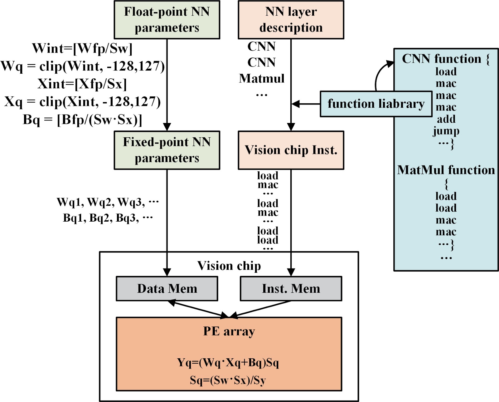
This paper describes a 2D/3D vision chip with integrated sensing and processing capabilities. The 2D/3D vision chip architecture includes a 2D/3D image sensor and a programmable visual processor. In this architecture, we design a novel on-chip processing flow with die-to-die image transmission and low-latency fixed-point image processing. The vision chip achieves real-time end-to-end processing of convolutional neural networks (CNNs) and conventional image processing algorithms. Furthermore, an end-to-end 2D/3D vision system is built to exhibit the capacity of the vision chip. The vision system achieves real-timing applications under 2D and 3D scenes, such as human face detection (processing delay 10.2 ms) and depth map reconstruction (processing delay 4.1 ms). The frame rate of image acquisition, image process, and result display is larger than 30 fps.

A 2D/3D vision chip based on organic substrate 3D package
Graphical Abstract
Original ResearchVol. 32, Issue 1 • pp. 100-112DOI: 10.1088/1674-4926/25010010Jan 15, 2025

Topological materials-based photodetectors from the infrared to terahertz range

Authors: Zhaowen Bao, Yiming Wang, Kaixuan Zhang, Yingdong Wei, Xiaokai Pan, Zhen Hu, Shiqi Lan, Yichong Zhang, Xiaoyun Wang, Huichuan Fan, Hongfei Wu, Lei Yang, Zhiyuan Zhou, Xin Sun, Yulu Chen, Lin Wang

Infrared and terahertz waves constitute pivotal bands within the electromagnetic spectrum, distinguished by their robust penetration capabilities and non-ionizing nature. These wavebands offer the potential for achieving high-resolution and non-destructive detection methodologies, thereby possessing considerable research significance across diverse domains including communication technologies, biomedical applications, and security screening systems. Two-dimensional materials, owing to their distinctive optoelectronic attributes, have found widespread application in photodetection endeavors. Nonetheless, their efficacy diminishes when tasked with detecting lower photon energies. Furthermore, as the landscape of device integration evolves, two-dimensional materials struggle to align with the stringent demands for device superior performance. Topological materials, with their topologically protected electronic states and non-trivial topological invariants, exhibit quantum anomalous Hall effects and ultra-high carrier mobility, providing a new approach for seeking photosensitive materials for infrared and terahertz photodetectors. This article introduces various types of topological materials and their properties, followed by an explanation of the detection mechanism and performance parameters of photodetectors. Finally, it summarizes the current research status of near-infrared to far-infrared photodetectors and terahertz photodetectors based on topological materials, discussing the challenges faced and future prospects in their development.

Topological materials-based photodetectors from the infrared to terahertz range
Graphical Abstract
Original ResearchVol. 32, Issue 1 • pp. 100-112DOI: 10.1088/1674-4926/25010002Jan 15, 2025

A K/Ka-band series Doherty CMOS power amplifier with distributed multi-step impedance inverting network

Authors: Xinyu Jiang, Wei Deng, Junlong Gong, Haikun Jia, Baoyong Chi

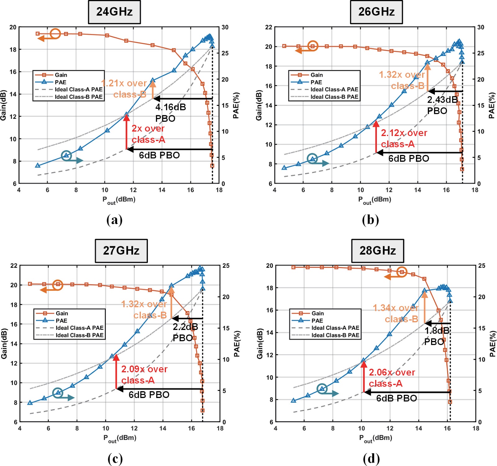
A two-way K/Ka-band series-Doherty PA (SDPA) with a distributed impedance inverting network (IIN) for millimeter wave applications is presented in this article. The proposed distributed IIN contributes to achieve wideband linear and power back-off (PBO) efficiency enhancement. Implemented in 65 nm bulk CMOS technology, this work realizes a measured 3 dB bandwidth of 15.5 GHz with 21.2 dB peak small-signal gain at 34.2 GHz. Under 1-V power supply, it achieves OP1dB over 13.4 dBm and Psat over 16 dBm between 21 to 30 GHz. The measured maximum Psat, OP1dB, peak/OP1dB/6dBPBO PAE results are 17.5, 14.7 dBm, and 28.2%/23.2%/13.2%. Without digital pre-distortion (DPD) and equalization, EVMs are lower than −25.2 dB for 200 MHz 64-QAM signals. Besides, this work achieves −33.35, −23.52, and −20 dB EVMs for 100 MHz 256-QAM, 600 MHz 64-QAM and 2 GHz 16-QAM signals at 27 GHz without DPD and equalization.

A K/Ka-band series Doherty CMOS power amplifier with distributed multi-step impedance inverting network
Graphical Abstract
Original ResearchVol. 32, Issue 1 • pp. 100-112DOI: 10.1088/1674-4926/25010028Jan 15, 2025

A battery-free wireless temperature sensing chipset implemented by 55 and 65 nm CMOS process

Authors: Jiayi Wang, Haoyang Li, Weixiao Wang, Tianying Fang, Jiaqing Li, Yuxuan Luo, Bo Zhao

In the applications such as food production, the environmental temperature should be measured continuously during the entire process, which requires an ultra-low-power temperature sensor for long-termly monitoring. Conventional temperature sensors trade the measurement accuracy with power consumption. In this work, we present a battery-free wireless temperature sensing chip for long-termly monitoring during food production. A calibrated oscillator-based CMOS temperature sensor is proposed instead of the ADC-based power-hungry circuits in conventional works. In addition, the sensor chip can harvest the power transferred by a remote reader to eliminate the use of battery. Meanwhile, the system conducts wireless bidirectional communication between the sensor chip and reader. In this way, the temperature sensor can realize both a high precision and battery-free operation. The temperature sensing chip is fabricated in 55 nm CMOS process, and the reader chip is implemented in 65 nm CMOS technology. Experimental results show that the temperature measurement error achieves ±1.6 °C from 25 to 50 °C, with battery-free readout by a remote reader.

A battery-free wireless temperature sensing chipset implemented by 55 and 65 nm CMOS process
Graphical Abstract
Original ResearchVol. 32, Issue 1 • pp. 100-112DOI: 10.1088/1674-4926/25010017Jan 15, 2025

Growth and optical properties of large-sized Co2+: ZnGa2O4 single crystal

Authors: Zhengyuan Li, Jiaqi Wei, Yiyuan Liu, Huihui Li, Yang Li, Zhitai Jia, Xutang Tao, Wenxiang Mu

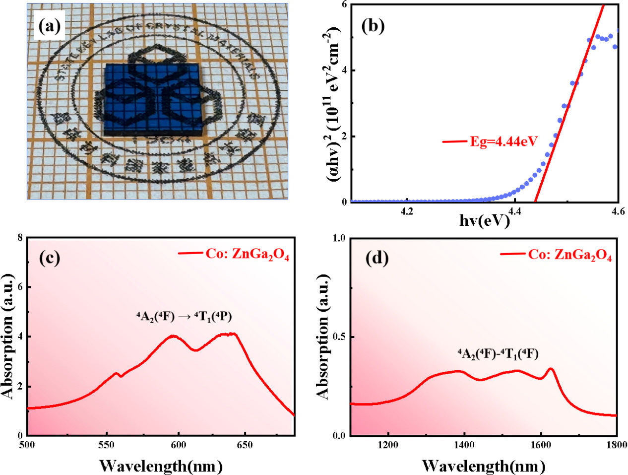
The transition of cobalt ions located at tetrahedral sites will produce strong absorption in the visible and near-infrared regions, and is expected to work in a passively Q-switched solid-state laser at the eye-safe wavelength of 1.5 µm. In this study, Co2+ ions were introduced into the wide bandgap semiconductor material ZnGa2O4, and large-sized and high-quality Co2+-doped ZnGa2O4 crystals with a volume of about 20 cm3 were grown using the vertical gradient freeze (VGF) method. Crystal structure and optical properties were analyzed using X-ray powder diffraction (XRD), X-ray photoelectron spectroscopy (XPS), and absorption spectroscopy. XRD results show that the Co2+-doped ZnGa2O4 crystal has a pure spinel phase without impurity phases and the rocking curve full width at half maximum (FWHM) is only 58 arcsec. The concentration of Co2+ in Co2+-doped ZnGa2O4 crystals was determined to be 0.2 at.% by the energy dispersive X-ray spectroscopy. The optical band gap of Co2+-doped ZnGa2O4 crystals is 4.44 eV. The optical absorption spectrum for Co2+-doped ZnGa2O4 reveals a prominent visible absorption band within 550−670 nm and a wide absorption band spanning from 1100 to 1700 nm. This suggests that the Co2+ ions have substituted the Zn2+ ions, which are typically tetrahedrally coordinated, within the lattice structure of ZnGa2O4. The visible region's absorption peak and the near-infrared broad absorption band are ascribed to the 4A2(4F) → 4T1(4P) and 4A2(4F) →4T1(4F) transitions, respectively. The optimal ground state absorption cross section was determined to be 3.07 × 10⁻¹⁹ cm2 in ZnGa2O4, a value that is comparatively large within the context of similar materials. This finding suggests that ZnGa2O4 is a promising candidate for use in near-infrared passive Q-switched solid-state lasers.

Growth and optical properties of large-sized Co2+: ZnGa2O4 single crystal
Graphical Abstract
Original ResearchVol. 32, Issue 1 • pp. 100-112DOI: 10.1088/1674-4926/25010022Jan 15, 2025

Research on heterojunction semiconductor photodetectors based on CsPbBr3 QDs/CsPbBrxI3–x QDs

Authors: Chenguang Shen, Mengwei Chen, Wei Huang, Yingping Yang

All-inorganic CsPbBr3 perovskite quantum dots (QDs) have attracted extensive attention in photoelectric detection for their excellent photoelectric properties and stability. However, the CsPbBr3 quantum dot film exhibits a high non-radiative recombination rate, and the mismatch in energy levels with the carbon electrode weakens hole extraction efficiency. These reduces the device's performance. To improve this, a semiconductor photodetector based on fluorine-doped tin oxide (FTO)/dense titanium dioxide (c-TiO2)/mesoporous titanium dioxide (m-TiO2)/CsPbBr3 QDs/CsPbBrxI3–x (x = 2, 1.5, 1) QDs/C structure was studied. By adjusting the Br– : I– ratio, the synthesized CsPbBrxI3–x (x = 2, 1.5, 1) QDs showed an adjustable band gap width of 2.284−2.394 eV. And forming a type Ⅱ band structure with CsPbBr3 QDs, which reduced the valence band offset between the active layer and the carbon electrode, this promoted carrier extraction and reduced non-radiative recombination rate. Compared with the original device (the photosensitive layer is CsPbBr3 QDs), the performance of the photodetector based on the CsPbBr3 QDs/CsPbBr2I QDs heterostructure is significantly improved, the responsivity (R) increased by 73%, the specific detectivity rate (D*) increased from 6.98 × 10¹² to 3.19 × 10¹³ Jones, the on/off ratio reached 106. This study provides a new idea for the development of semiconductor tandem detectors.

Research on heterojunction semiconductor photodetectors based on CsPbBr3 QDs/CsPbBrxI3–x QDs
Graphical Abstract
Original ResearchVol. 32, Issue 1 • pp. 100-112DOI: 10.1088/1674-4926/25010021Jan 15, 2025

Interface energetics in organic and perovskite semiconductor solar cells

Authors: Shaobing Xiong, Mats Fahlman, Qinye Bao

Improving the quality of life for Earth’s growing population is a complex task that requires the development of new technologies and materials. Perhaps the biggest challenge is access to clean and renewable energy sources that can drive a sustainable future. Photovoltaics, today mainly represented by silicon-based solar cells, convert solar energy into electricity and is already an important component in the renewable energy portfolio. Organic solar cells (OSCs) and perovskite solar cells (PSCs) both offer advantages compared to silicon solar cells such as low-temperature solution processing, flexibility and semi-transparency while sharing similar device structures consisting of a photoactive layer (PAL) sandwiched between an anode and a cathode contact. The anode and cathode contacts in OSCs and PSCs typically consist of a charge transport layer (CTL) and a conductor (often a metal), and the CTLs significantly impact device performance. The CTLs used in OSCs and PSCs share many functionalities. OSCs and PSCs fabrication involves sequential deposition of layers from solution and treatments at elevated temperatures, so the CTLs must be solvent resistant and stable under thermal cycling (also important for long-term device stability). Preferably, the CTLs should also have sufficient tolerance to thickness variations to facilitate roll-to-roll fabrication. The CTL requirements however differ for OSCs and PSCs due to the unique respective properties of the organic semiconductor and metal halide perovskite PALs, so we will discuss them separately below.

Interface energetics in organic and perovskite semiconductor solar cells
Graphical Abstract
Original ResearchVol. 32, Issue 2 • pp. 100-112DOI: 10.1088/1674-4926/25020010Jan 15, 2025

A 128 × 128 monolithic spike-based hybrid-vision sensor with 0.96 Geps and 117 kfps

Authors: Huanhui Zhang, Chi Zhang, Xu Yang, Zhe Wang, Cong Shi, Runjiang Dou, Shuangming Yu, Jian Liu, Nanjian Wu, Peng Feng, Liyuan Liu

The event-based vision sensor (EVS), which can generate efficient spiking data streams by exclusively detecting motion, exemplifies neuromorphic vision methodologies. Generally, its inherent lack of texture features limits effectiveness in complex vision processing tasks, necessitating supplementary visual information. However, to date, no event-based hybrid vision solution has been developed that preserves the characteristics of complete spike data streams to support synchronous computation architectures based on spiking neural network (SNN). In this paper, we present a novel spike-based sensor with digitized pixels, which integrates the event detection structure with the pulse frequency modulation (PFM) circuit. This design enables the simultaneous output of spiking data that encodes both temporal changes and texture information. Fabricated in 180 nm process, the proposed sensor achieves a resolution of 128 × 128, a maximum event rate of 960 Meps, a grayscale frame rate of 117.1 kfps, and a measured power consumption of 60.1 mW, which is suited for high-speed, low-latency, edge SNN-based vision computing systems.

A 128 × 128 monolithic spike-based hybrid-vision sensor with 0.96 Geps and 117 kfps
Graphical Abstract
Original ResearchVol. 32, Issue 2 • pp. 100-112DOI: 10.1088/1674-4926/25020014Jan 15, 2025

GaN diodes comparative study for high energy protons detection

Authors: Matilde Siviero, Maxime Hugues, Lucas Lesourd, Eric Frayssinet, Shirley Prado de la Cruz, Sebastien Chenot, Johan-Petter Hofverberg, Marie Vidal, Jean-Yves Duboz

GaN diodes for high energy (64.8 MeV) proton detection were fabricated and investigated. A comparison of the performance of GaN diodes with different structures is presented, with a focus on sapphire and on GaN substrates, Schottky and pin diodes, and different active layer thicknesses. Pin diodes fabricated on a sapphire substrate are the best choice for a GaN proton detector working at 0 V bias. They are sensitive (minimum detectable proton beam <1 pA/cm2), linear as a function of proton current and fast (<1 s). High proton current sensitivity and high spatial resolution of GaN diodes can be exploited in the future for proton imaging of patients in proton therapy.

GaN diodes comparative study for high energy protons detection
Graphical Abstract
Original ResearchVol. 32, Issue 2 • pp. 100-112DOI: 10.1088/1674-4926/25020006Jan 15, 2025

Dynamic avalanche reliability enhancement of FS-IGBT under unclamped inductive switching

Authors: Jingping Zhang, Houcai Luo, Huan Wu, Bofeng Zheng, Xianping Chen

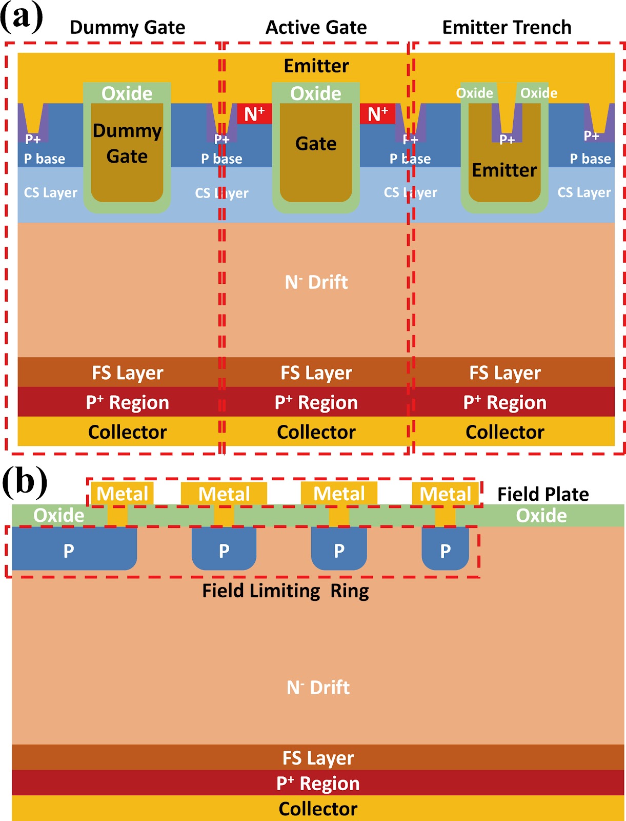
The dynamic avalanche effect is a critical factor influencing the performance and reliability of the field-stop insulated gate bipolar transistors (FS-IGBT). Unclamped inductive switching (UIS) is the primary method for testing the dynamic avalanche capability of FS-IGBTs. Numerous studies have demonstrated that factors such as device structure, avalanche-generating current filaments, and electrical parameters influence the dynamic avalanche effect of the FS-IGBT. However, few studies have focused on enhancing the avalanche reliability of the FS-IGBT by adjusting circuit parameters during operation. In this paper, the dynamic avalanche effect of the FS-IGBT under UIS conditions is comprehensively investigated through a series of comparative experiments with varying circuit parameters, including bus voltage VDC, gate voltage VG, gate resistance Rg, load inductance L, and temperature TC. Furthermore, a method to enhance the dynamic avalanche reliability of the FS-IGBT under UIS by optimizing circuit parameters is proposed. In practical applications, reducing gate voltage, increasing load inductance, and lowering temperature can effectively improve the dynamic avalanche capability of the FS-IGBT.

Dynamic avalanche reliability enhancement of FS-IGBT under unclamped inductive switching
Graphical Abstract
Original ResearchVol. 32, Issue 2 • pp. 100-112DOI: 10.1088/1674-4926/25020029Jan 15, 2025

A miniaturized wireless electrical impedance myography platform for the long-term adaptive muscle fatigue monitoring

Authors: Shanshan Yu, Yichao Gan, Feifan Song, Qiongzhang Wang, Hao Tang, Zhao Li

Accurate quantification of exercise interventions and changes in muscle function is essential for personalized health management. Electrical impedance myography (EIM) technology offers an innovative, noninvasive, painless, and easy-to-perform solution for muscle health monitoring. However, current EIM platforms face a number of limitations, including large device size, wired connections, and instability of the electrode-skin interface, which limit their applicability for monitoring muscle movement. In this study, a miniature wireless EIM platform with a user-friendly smartphone app is proposed and developed. The miniature, wireless, multi-frequency (20 kHz−1 MHz) EIM platform is equipped with flexible microneedle array electrodes (MAE). The advantages of MAEs over conventional electrodes were demonstrated by physical field modeling simulations and skin-electrode contact impedance comparison tests. The smartphone APP was developed to wirelessly operate the EIM platform, and to transmit and process real-time muscle impedance data. To validate its effectiveness, a seven-day adaptive fatigue training study was conducted, which demonstrated that the EIM platform was able to detect muscle adaptations and serve as a reliable indicator of fatigue. This study presents an innovative approach to applying EIM technology to muscle health monitoring and exercise testing, thereby advancing the development of personalized health management and athletic performance assessment.

A miniaturized wireless electrical impedance myography platform for the long-term adaptive muscle fatigue monitoring
Graphical Abstract
Original ResearchVol. 32, Issue 2 • pp. 100-112DOI: 10.1088/1674-4926/25020018Jan 15, 2025

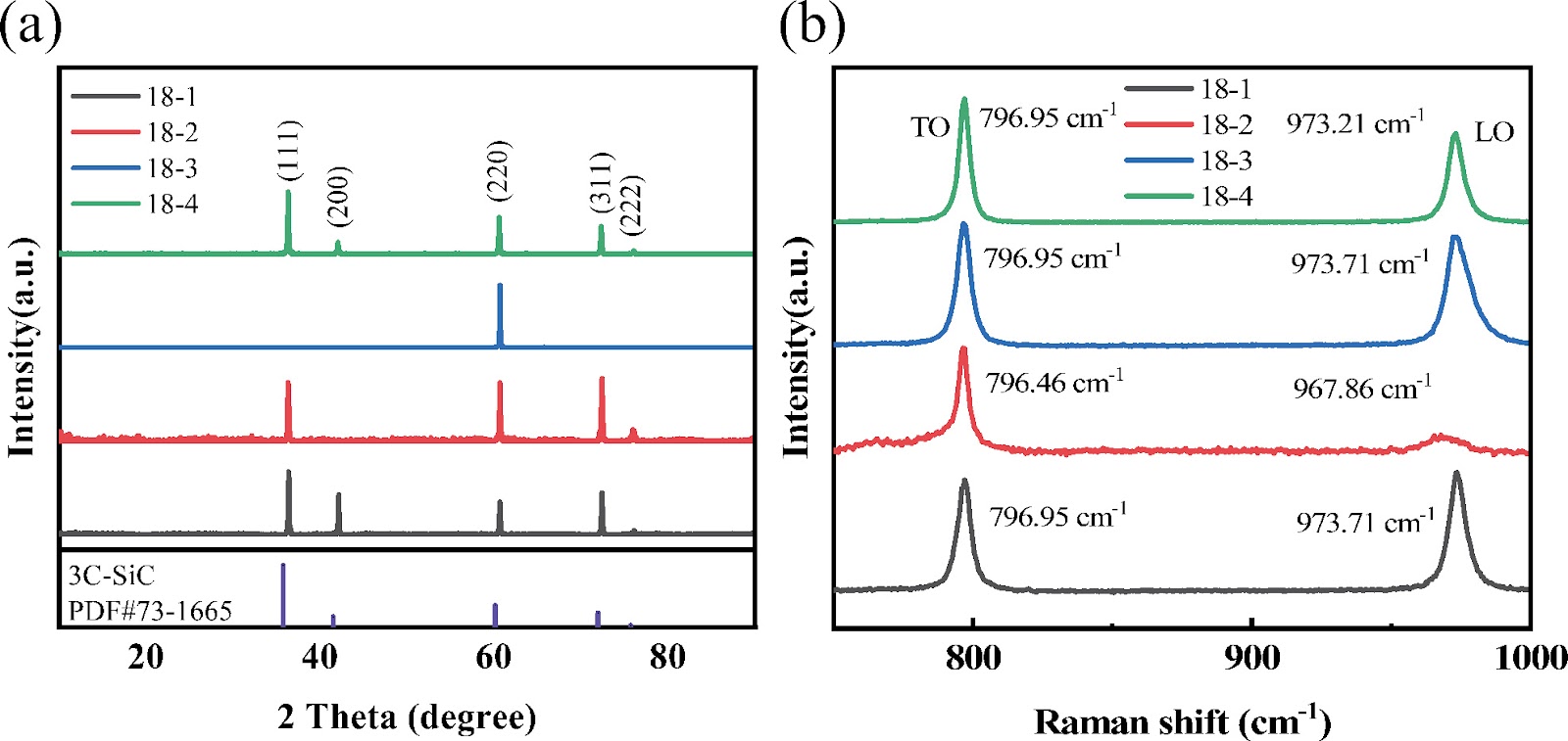
Effect of grain size on the resistivity of polycrystalline 3C-SiC

Authors: Guo Li, Lei Ge, Mingsheng Xu, Jisheng Han, Xiangang Xu

Silicon carbide offers distinct advantages in the field of power electronic devices. However, manufacturing processes remain a significant barrier to its widespread adoption. Polycrystalline SiC is less expensive and easier to produce than single crystal. But stabilizing and controlling its performance are critical challenges that must be addressed urgently. Due to its material properties and excellent performance in applications, 3C-SiC is gaining increasing attention in research. This article presents the electrical and material properties of a series of polycrystalline 3C-SiC samples and investigates their interrelationship. The samples were examined using TEM, which confirmed their polycrystalline structure. Combined with XRD and Raman spectroscopy, the grain orientations within the samples were analyzed, and the presence of stress was verified. EBSD was employed to statistically examine the grain structure and size across samples. For samples with similar doping levels, grain size is the most influential factor in determining electrical characteristics. Further EBSD measurements reveal the relationship between resistivity and grain size as log(ρ) = −1.93 + 8.67/d. These findings provide a foundation for the quantitative control and application of polycrystalline 3C-SiC. This work offers theoretical evidence for optimizing the performance tuning of 3C-SiC ceramics and enhancing their effectiveness in electronic applications.

Effect of grain size on the resistivity of polycrystalline 3C-SiC
Graphical Abstract
Original ResearchVol. 32, Issue 2 • pp. 100-112DOI: 10.1088/1674-4926/25020033Jan 15, 2025

Study of a novel SiC-based light initiated multi-gate semiconductor switch

Authors: Chongbiao Luan, Jianqiang Yuan, Hongwei Liu, Longfei Xiao, Huiru Sha, Le Xu, Yang He, Lingyun Wang, Hongtao Li, Yupeng Huang

To optimize turn on velocity of the SiC LIMS, we proposed a new structure for the LIMS that incorporates an optimized n+ layer and a multi-light triggered electrode design for the anode. The chip size is 5.5 mm × 5.5 mm in dimension. The experiment results indicate that the saturation laser energy required to trigger the prepared SiC LIMS has been decreased from 1.8 mJ to 40 μJ, with the forward blocking voltage of the prepared SiC LIMSs capable of withstanding over 7000 V. The leakage current is about 0.3 μA at room temperature, and the output current density achieves 4.25 kA/cm2 (with di/dt larger than 20 kA/μs).

Study of a novel SiC-based light initiated multi-gate semiconductor switch
Graphical Abstract
Original ResearchVol. 32, Issue 2 • pp. 100-112DOI: 10.1088/1674-4926/25020031Jan 15, 2025

Breathable and skin-conformal electronic skin with dual-modality synchronous perception of pressure and temperature

Authors: Hao Zhu, Zhelin Jin, Tie Li, Guanggui Cheng, Jianning Ding

The random nanofiber distribution in traditional electrospun membranes restricts the pressure sensing sensitivity and measurement range of electronic skin. Moreover, current multimodal sensing suffers from issues like overlapping signal outputs and slow response. Herein, a novel electrospinning method is proposed to prepare double-coupled microstructured nanofibrous membranes. Through the effect of high voltage electrostatic field in the electrospinning, the positively charged nanofibers are preferentially attached to the negatively charged foam surface, forming the ordered two-dimensional honeycomb porous nanofibrous membrane with three-dimensional spinous microstructure. Compared with the conventional random porous nanofibrous membrane, the bionic two-dimensional honeycomb and three-dimensional spinous dual-coupled microstructures in the ordered porous nanofibrous membrane endows the electronic skin with significantly improved mechanical properties (maximum tensile strain increased by 77% and fatigue resistance increased by 35%), air permeability (water vapor transmission rate increased by 16%) and sensing properties (pressure sensitivity increased by 276% and detection range increased by 137%). Furthermore, the electronic skin was constructed by means of a conformal composite ionic liquid functionalized nanofibrous membrane, and the real-time and interference-free dual-signal monitoring of pressure and temperature (maximum temperature coefficient of resistance: −0.918 °C−1) was realized.

Breathable and skin-conformal electronic skin with dual-modality synchronous perception of pressure and temperature
Graphical Abstract
Original ResearchVol. 32, Issue 2 • pp. 100-112DOI: 10.1088/1674-4926/25020025Jan 15, 2025

Mesa-structured AlGaAsSb APD: dark current and noise analysis

Authors: Yuhang He, Rui Wang, Yan Liang, Yingqiang Xu, Guowei Wang, Haiqiao Ni, Shuo Wang, Zhichuan Niu, Xiaohong Yang

Avalanche photodiode (APD) is a kind of photodetector with important applications in optical communication, light detection and ranging (LIDAR) and other fields. APDs fabricated using the recently developed AlGaAsSb as the multiplication material exhibit excellent noise performance. In this work, we report a low-noise separate absorption, grading, charge, and multiplication (SAGCM) InGaAs/AlGaAsSb APD operating at 1550 nm. A double-mesa structure was fabricated to reduce the dark current. Numerical simulations were conducted to compare two different mesa-structured APDs. By analyzing the electric field distribution, it was found that the electric field at the edge of the multiplication region in the double-mesa APD is nearly 100 kV/cm lower than that of the single-mesa structure. Experimental results demonstrate that after device punch-through, the double-mesa APD’s dark current can be reduced by up to four times compared to the single-mesa APD. Quantitative analysis of the dark current components in the AlGaAsSb APD further confirms that the low sidewall electric field in the double-mesa structure effectively suppresses the trap-assisted tunneling. Additionally, noise measurements indicate a k-value of approximately 0.014, which is significantly lower than that of traditional multiplication materials. This work provides preliminary validation for further performance improvements in low noise and low dark current AlGaAsSb APDs.

Mesa-structured AlGaAsSb APD: dark current and noise analysis
Graphical Abstract
Original ResearchVol. 32, Issue 2 • pp. 100-112DOI: 10.1088/1674-4926/25020008Jan 15, 2025

Band alignment of SnO/β-Ga2O3 heterojunction and its electrical properties for power device application

Authors: Xia Wu, Chenyang Huang, Xiuxing Xu, Jun Wang, Xinwang Yao, Yanfang Liu, Xiujuan Wang, Chunyan Wu, Linbao Luo

In this study, we present the fabrication of vertical SnO/β-Ga2O3 heterojunction diode (HJD) via radio frequency (RF) reactive magnetron sputtering. The valence and conduction band offsets between β-Ga2O3 and SnO are determined to be 2.65 and 0.75 eV, respectively, through X-ray photoelectron spectroscopy, showing a type-Ⅱ band alignment. Compared to its Schottky barrier diode (SBD) counterpart, the HJD presents a comparable specific ON-resistances (Ron,sp) of 2.8 mΩ·cm² and lower reverse leakage current (IR), leading to an enhanced reverse blocking characteristics with breakdown voltage (BV) of 1675 V and power figure of merit (PFOM) of 1.0 GW/cm². This demonstrates the high quality of the SnO/β-Ga2O3 heterojunction interface. Silvaco TCAD simulation further reveals that electric field crowding at the edge of anode for the SBD was greatly depressed by the introduction of SnO film, revealing the potential application of SnO/β-Ga2O3 heterojunction in the future β-Ga2O3-based power devices.

Band alignment of SnO/β-Ga2O3 heterojunction and its electrical properties for power device application
Graphical Abstract
Original ResearchVol. 32, Issue 2 • pp. 100-112DOI: 10.1088/1674-4926/25020028Jan 15, 2025

A leap forward in compute-in-memory system for neural network inference

Authors: Liang Chu, Wenjun Li

Developing efficient neural network (NN) computing systems is crucial in the era of artificial intelligence (AI). Traditional von Neumann architectures have both the issues of "memory wall" and "power wall", limiting the data transfer between memory and processing units. Compute-in-memory (CIM) technologies, particularly analogue CIM with memristor crossbars, are promising because of their high energy efficiency, computational parallelism, and integration density for NN computations. In practical applications, analogue CIM excels in tasks like speech recognition and image classification, revealing its unique advantages. For instance, it efficiently processes vast amounts of audio data in speech recognition, achieving high accuracy with minimal power consumption. In image classification, the high parallelism of analogue CIM significantly speeds up feature extraction and reduces processing time. With the boosting development of AI applications, the demands for computational accuracy and task complexity are rising continually. However, analogue CIM systems are limited in handling complex regression tasks with needs of precise floating-point (FP) calculations. They are primarily suited for the classification tasks with low data precision and a limited dynamic range. A novel analogue-digital unified CIM architecture (named as AnDi) has been developed by integrating the analogue and digital computing cores, which aims to address the above challenges of analogue CIM. The key component is the dual-domain floating-point (DDFP) processor, which serves as a universal data type to represent both FP and integer (INT) numbers. This processor enables FP compatibility regardless of the native capabilities of analogue CIM or digital cores. The DDFP data structure consists of an INT tensor for the feature map and an FP scale. The DDFP processor manages data flow between the analogue and digital domains, performing quantization or dequantization operation. This effectively decouples the NN algorithm from the underlying hardware, enabling more general NN computation. The training process for the top-level algorithm can proceed without considering specific hardware architectures, as all data-scaling operations are handled at the hardware level. To maximize the potential of AnDi architecture, several strategies have been proposed. The fine-grained dual-domain mapping divides weight matrices larger than analogue CIM arrays into smaller ones. Weights are allocated to either digital or analogue cores based on their size. Low-parallel weight blocks are assigned to digital cores, thus maximizing the utilization rates of digital multiply-accumulate (MAC) cores. This approach enhances system-level energy efficiency by avoiding weight splits into additional blocks within the same layer, thereby reducing memory management overhead. The NN feature-enhancing technique addresses the noise accumulation issue in analogue CIM. Lightweight enhancing layers are integrated into the network and deployed on noise-free digital cores for inference.

A leap forward in compute-in-memory system for neural network inference
Graphical Abstract
Original ResearchVol. 32, Issue 2 • pp. 100-112DOI: 10.1088/1674-4926/25020024Jan 15, 2025

Boosting photoelectrochemical performance on α-Ga2O3 nanowire arrays by indium cation doping for self-powered ultraviolet detection

Authors: Junjun Xue, Jiyuan Huang, Kehan Li, Ping Liu, Yan Gu, Ting Zhi, Yan Dong, Jin Wang

Low power consumption, high responsivity, and self-powering are key objectives for photoelectrochemical ultraviolet detectors. In this research, In-doped α-Ga2O3 nanowire arrays were fabricated on fluorine-doped tin oxide (FTO) substrates through a hydrothermal approach, with subsequent thermal annealing. These arrays were then used as photoanodes to construct a ultraviolet (UV) photodetector. In doping reduced the bandgap of α-Ga2O3, enhancing its absorption of UV light. Consequently, the In-doped α-Ga2O3 nanowire arrays exhibited excellent light detection performance. When irradiated by 255 nm deep ultraviolet light, they obtained a responsivity of 38.85 mA/W. Moreover, the detector's response and recovery times are 13 and 8 ms, respectively. The In-doped α-Ga2O3 nanowire arrays exhibit a responsivity that is about three-fold higher than the undoped one. Due to its superior responsivity, the In-doped device was used to develop a photoelectric imaging system. This study demonstrates that doping α-Ga2O3 nanowire with indium is a potent approach for optimizing their photoelectrochemical performance, which also has significant potential for optoelectronic applications.

Boosting photoelectrochemical performance on α-Ga2O3 nanowire arrays by indium cation doping for self-powered ultraviolet detection
Graphical Abstract
Original ResearchVol. 32, Issue 2 • pp. 100-112DOI: 10.1088/1674-4926/25020011Jan 15, 2025

A 32Gb/s digital-assisted PAM-4 DFB laser driver in 28-nm CMOS

Authors: Yang Min, Nan Qi, Yihan Chen, Minye Zhu, Guike Li, Yonghui Lin, Zhao Zhang, Jian Liu, Nanjian Wu, Jingbo Shi, Frank F. Shi, Liyuan Liu

This paper presents a 4-level pulse amplitude modulation (PAM-4) distributed feedback (DFB) laser driver. The driver adopts a digital slicing architecture to achieve high linearity by adjusting the weights of three thermometer-coded main paths. An efficient-biased output stage structure is proposed to reduce power consumption while avoiding the degradation of output node bandwidth typically induced by parasitic capacitance in high-current bias path. A two-tap linear and nonlinear feed-forward equalizer (FFE) is implemented in the digital domain to extend bandwidth limitations and compensate for the dynamic nonlinearity of the DFB laser. The nonlinear FFE is realized at the cost of lower power consumption and smaller area by utilizing the simultaneity of low-speed parallel data. The chip is fabricated in 28 nm CMOS process. Measurement results indicate that, with a laser bias current of 40 mA, a modulation current of 20 mApp, and an operating rate of 32 Gb/s PAM-4, the overall power consumption of the chip is 372 mW, corresponding to an energy efficiency of 11.6 pJ/b.

A 32Gb/s digital-assisted PAM-4 DFB laser driver in 28-nm CMOS
Graphical Abstract
Original ResearchVol. 32, Issue 2 • pp. 100-112DOI: 10.1088/1674-4926/25020034Jan 15, 2025

Robotic computing system and embodied AI evolution: an algorithm-hardware co-design perspective

Authors: YAN Longke, ZHAO Xin, YANG Bohan, WU Yongkun, DAI Guangnan, LI Jiancong, TSUI Chi-Ying, CHENG Kwang-Ting, ZHANG Yihan, TU Fengbin

Robotic computing systems play an important role in enabling intelligent robotic tasks through intelligent algorithms and supporting hardware. In recent years, the evolution of robotic algorithms indicates a roadmap from traditional robotics to hierarchical and end-to-end models. This algorithmic advancement poses a critical challenge in achieving balanced system-wide performance. Therefore, algorithm-hardware co-design has emerged as the primary methodology, which analyzes algorithm behaviors on hardware to identify common computational properties. These properties can motivate algorithm optimization to reduce computational complexity and hardware innovation from architecture to circuit for high performance and high energy efficiency. We then reviewed recent works on robotic and embodied AI algorithms and computing hardware to demonstrate this algorithm-hardware co-design methodology. In the end, we discuss future research opportunities by answering two questions: (1) how to adapt the computing platforms to the rapid evolution of embodied AI algorithms, and (2) how to transform the potential of emerging hardware innovations into end-to-end inference improvements.

Robotic computing system and embodied AI evolution: an algorithm-hardware co-design perspective
Graphical Abstract
Original ResearchVol. 32, Issue 3 • pp. 100-112DOI: 10.1088/1674-4926/25030009Jan 15, 2025

Self-assembled flexible Ti3C2Tx MXene-based thermally chargeable supercapacitor

Authors: Lifeng Wu, La Li, Guozhen Shen

Thermally chargeable supercapacitors (TCSCs) have unique advantages in the collection, conversion, and storage of thermal energy, contributing to the development of new strategies for thermal energy utilization. 2D MXene materials are predicted to be highly promising new thermoelectric materials. Here, we report a self-assembled flexible Ti3C2Tx MXene-based TCSC device, using prepared Ti3C2Tx MXene as the capacitor electrode and a NaClO4/PEO gel as the electrolyte. We also explore the working mechanism of the TCSCs. The fabricated Ti3C2Tx-based TCSCs exhibit an excellent Seebeck coefficient of 11.8 mV∙K−1 on average and maintain good cycling stability under various temperature differences. Demonstrations of multiple practical applications show that Ti3C2Tx MXene-based TCSC devices are excellent candidates for self-powered integrated electronic devices.

Self-assembled flexible Ti3C2Tx MXene-based thermally chargeable supercapacitor
Graphical Abstract
Original ResearchVol. 32, Issue 3 • pp. 100-112DOI: 10.1088/1674-4926/25030023Jan 15, 2025

Nucleation control for the growth of two-dimensional single crystals

Authors: Jinxia Bai, Chi Zhang, Fankai Zeng, Jinzong Kou, Jinhuan Wang, Xiaozhi Xu

The unique structure and exceptional properties of two-dimensional (2D) materials offer significant potential for transformative advancements in semiconductor industry. Similar to the reliance on wafer-scale single-crystal ingots for silicon-based chips, practical applications of 2D materials at the chip level need large-scale, high-quality production of 2D single crystals. Over the past two decades, the size of 2D single-crystals has been improved to wafer or meter scale, where the nucleation control during the growth process is particularly important. Therefore, it is essential to conduct a comprehensive review of nucleation control to gain fundamental insights into the growth of 2D single-crystal materials. This review mainly focuses on two aspects: controlling nucleation density to enable the growth from a single nucleus, and controlling nucleation position to achieve the unidirectionally aligned islands and subsequent seamless stitching. Finally, we provide an overview and forecast of the strategic pathways for emerging 2D materials.

Nucleation control for the growth of two-dimensional single crystals
Graphical Abstract
Original ResearchVol. 32, Issue 3 • pp. 100-112DOI: 10.1088/1674-4926/25030003Jan 15, 2025

Synthesis of p-type PbS quantum dot ink via inorganic ligand exchange in solution for high-efficiency and stable solar cells

Authors: Napasuda Wichaiyo, Yuyao Wei, Chao Ding, Guozheng Shi, Witoon Yindeesuk, Liang Wang, Huān Bì, Jiaqi Liu, Shuzi Hayase, Yusheng Li, Yongge Yang, Qing Shen

Traditional p-type colloidal quantum dot (CQD) hole transport layers (HTLs) used in CQD solar cells (CQDSCs) are commonly based on organic ligands exchange and the layer-by-layer (LbL) technique. Nonetheless, the ligand detachment and complex fabrication process introduce surface defects, compromising device stability and efficiency. In this work, we propose a solution-phase ligand exchange (SPLE) method utilizing inorganic ligands to develop stable p-type lead sulfide (PbS) CQD inks for the first time. Various amounts of tin (II) iodide (SnI2) were mixed with lead halide (PbX2; X = I, Br) in the ligand solution. By precisely controlling the SnI₂ concentration, we regulate the transition of PbS QDs from n-type to p-type. PbS CQDSCs were fabricated using two different HTL approaches: one with 1,2-ethanedithiol (EDT)-passivated QDs via the LbL method (control) and another with inorganic ligand-passivated QD ink (target). The target devices achieved a higher power conversion efficiency (PCE) of 10.93%, compared to 9.83% for the control devices. This improvement is attributed to reduced interfacial defects and enhanced carrier mobility. The proposed technique offers an efficient pathway for producing stable p-type PbS CQD inks using inorganic ligands, paving the way for high-performance and flexible CQD-based optoelectronic devices.

Synthesis of p-type PbS quantum dot ink via inorganic ligand exchange in solution for high-efficiency and stable solar cells
Graphical Abstract
Original ResearchVol. 32, Issue 3 • pp. 100-112DOI: 10.1088/1674-4926/25030012Jan 15, 2025

Manipulation strategy of cation inhomogeneity in perovskite solar cells

Authors: Jiale Sun, Xuxia Shai, Weitao Chen, Shenchao Li, Jinlan He, Xinxing Liu, Dongmei He, Yue Yu, Jiangzhao Chen

In recent years, research advancements have highlighted the critical role of the A-site cation in determining the optoelectronic and physicochemical properties of organic–inorganic lead halide perovskites. Mixed-cation perovskites (MCPs) have been extensively used as absorber thin films in perovskite solar cells (PSCs), achieving high power conversion efficiencies (PCE) over 26%. The incorporation of mixed cations has led to a more optimal tolerance factor for the crystal structure, enhancing structural stability and providing additional functionalities to improve the chemical stability of the absorber thin films. However, mixed-cation perovskite absorbers often experience element and phase segregation, which can reduce device efficiency and operational lifespan. This segregation is a widespread phenomenon observed across various types of MCPs, whether in 2D or 3D structures. Therefore, understanding the fundamental causes of non-uniformity and phase segregation, as well as effective nanoscale regulatory strategies, is essential for enhancing the performance of PSCs. The development of high-quality MCPs with highly uniform cation distribution and stable phases is critical for addressing the stability challenges in PSCs.

Manipulation strategy of cation inhomogeneity in perovskite solar cells
Graphical Abstract
Original ResearchVol. 32, Issue 3 • pp. 100-112DOI: 10.1088/1674-4926/25030001Jan 15, 2025

A 112 Gbps DSP-based PAM4 SerDes receiver with a wide band equalization tuning AFE in 7 nm FinFET

Authors: Huanan Guo, Yufeng Yao, Jiazhen Ni, Xiang Gao

In DSP-based SerDes application, it is essential for AFE to implement a pre-ADC equalization to provide a better signal for ADC and DSP. To meet the various equalization requirements of different channel and transmitter configurations, this paper presents a 112 Gbps DSP-Based PAM4 SerDes receiver with a wide band equalization tuning AFE. The AFE is realized by implementing source degeneration transconductance, feedforward high-pass branch and inductive feedback peaking TIA. The AFE offers a flexible equalization gain tuning of up to 17.5 dB at Nyquist frequency without affecting the DC gain. With the proposed AFE, the receiver demonstrates eye opening after digital FIR equalization and achieves 6 × 10⁻⁹ BER with a 29.6 dB insertion loss channel.

A 112 Gbps DSP-based PAM4 SerDes receiver with a wide band equalization tuning AFE in 7 nm FinFET
Graphical Abstract
Original ResearchVol. 32, Issue 3 • pp. 100-112DOI: 10.1088/1674-4926/25030025Jan 15, 2025

CZTS based novel bifunctional photovoltaic and self-powered photodetection nano system

Authors: Kalyan B. Chavan, Maruti V. Salve, Shweta Chaure, Nandu B. Chaure

CZTS (Cu2ZnSnS4) is a quaternary semiconductor that is environmentally friendly, less expensive. In this paper, we report on the optimization and fabrication of CZTS-based heterojunction nanodevices for bifunctional applications such as solar cells and photodetectors. CZTS thin films were deposited on top of (Molybdenum) Mo-coated glass substrates via RF sputtering at 100 and 200 W. Rapid thermal processing (RTP) was used at 300, 400, and 500 °C temperatures. CdS (cadmium sulphide) was deposited on CZTS using a chemical bath deposition system with 3- and 5-min deposition times. ZnO (zinc oxide) and AZO (aluminium doped zinc oxide) layers were deposited using RF (radio frequency) sputtering to create the solar device. XRD confirms the formation of a tetragonal structure with increased crystallinity due to the use of RTP. Raman reveals the characteristic Raman shift peak associated with CZTS at 336 and 335 cm−1. The FESEM shows a relationship with RTP temperature. Surface features, including grain size, vary with RTP temperature. The ideality factor is nearly 2, indicating imperfection in the Mo/CZTS interface. Schottky barrier height estimates range from 0.6 to 0.7 eV. Absorbance and transmittance show a predictable fluctuation with RTP temperature. Photovoltaic device was built using the higher crystalline feature of CZTS in conjunction with CdS deposited at 3 and 5 min. The efficiency of CdS deposited after 3 and 5 min was 1.15 and 0.97 percent, respectively. Fabricated devices were used for wavelength-dependent photodetection. This work demonstrated self-powered photodetection.

CZTS based novel bifunctional photovoltaic and self-powered photodetection nano system
Graphical Abstract
Original ResearchVol. 32, Issue 3 • pp. 100-112DOI: 10.1088/1674-4926/25030041Jan 15, 2025

Effect of nitrogen incorporation and surface passivation on photoluminescence properties of InAs-based nanowires

Authors: Ratmir Ustimenko, Danila Karaulov, Maxim Vinnichenko, Ilya Norvatov, Andrey Kaveev, Vladimir Fedorov, Ivan Mukhin, Dmitry Firsov

InAsN nanowires on InAs stems were obtained using plasma-assisted molecular beam epitaxy on a SiOx/Si (111) substrate. Also, heterostructured InAs/InAsN and InAsN/InP nanowires were grown in the core/shell geometry. In the low-temperature photoluminescence spectra of the grown structures, spectral features are observed that correspond to the polytypic structure of nanowires with a predominance of the wurtzite phase and parasitic islands of the sphalerite phase. It was shown that the interband photoluminescence spectral features of InAsN nanowires experience a red shift relative to the pristine InAs nanowires. The incorporation of nitrogen reduces the bandgap by splitting the conduction band into two subbands. The position of the spectral features in the photoluminescence spectra confirms the formation of a nitride solid solution with a polytypic hexagonal structure, having a concentration of nitrogen atoms of up to 0.7%. Additional passivation of the nanowire surface with InP leads to a decrease in the intensity of nonradiative recombination and an improvement in the photoluminescent response of the nanowires, which makes it possible to detect photoluminescence emission at room temperature. Thus, by changing the composition and morphology of nanowires, it is possible to control their electronic structure, which allows varying the operating range of detectors and mid-IR radiation sources based on them.

Effect of nitrogen incorporation and surface passivation on photoluminescence properties of InAs-based nanowires
Graphical Abstract
Original ResearchVol. 32, Issue 3 • pp. 100-112DOI: 10.1088/1674-4926/25030801Jan 15, 2025

Preface to Special Topic on Quantum Dot Semiconductor Optoelectronic Materials, Devices, and Characterization

Authors: Zeke Liu, Wanli Ma

The discovery and synthesis of colloidal quantum dots (QDs) were awarded the 2023 Nobel Prize in Chemistry. QDs, as a novel class of materials distinct from traditional molecular materials and bulk materials, have rapidly emerged in the field of optoelectronic applications due to their unique size-, composition-, surface-, and process-dependent optoelectronic properties. More importantly, their ultra-high specific surface area allows for the application of various surface chemical engineering techniques to regulate and optimize their optoelectronic performance. Furthermore, three-dimensionally confined QDs can achieve nearly perfect photoluminescence quantum yields and extended hot carrier cooling times. Particularly, their ability to be colloidally synthesized and processed using industrially friendly solvents is driving transformative changes in the fields of electronics, photonics, and optoelectronics. In this Special Topic, we have selected four typical types of QD materials and their optoelectronic applications, including 4 Research Articles and 1 Review, to introduce the latest research advances in QD materials and optoelectronic fields.

Preface to Special Topic on Quantum Dot Semiconductor Optoelectronic Materials, Devices, and Characterization
Graphical Abstract
Original ResearchVol. 32, Issue 3 • pp. 100-112DOI: 10.1088/1674-4926/25030015Jan 15, 2025

High-speed electro-absorption modulated laser

Authors: Zhenyao Li, Chen Lyu, Xuliang Zhou, Mengqi Wang, Haotian Qiu, Yejin Zhang, Hongyan Yu, Jiaoqing Pan

Currently, the global 5G network, cloud computing, and data center industries are experiencing rapid development. The continuous growth of data center traffic has driven the vigorous progress in high-speed optical transceivers for optical interconnection within data centers. The electro-absorption modulated laser (EML), which is widely used in optical fiber communications, data centers, and high-speed data transmission systems, represents a high-performance photoelectric conversion device. Compared to traditional directly modulated lasers (DMLs), EMLs demonstrate lower frequency chirp and higher modulation bandwidth, enabling support for higher data rates and longer transmission distances. This article introduces the composition, working principles, manufacturing processes, and applications of EMLs. It reviews the progress on advanced indium phosphide (InP)-based EML devices from research institutions worldwide, while summarizing and comparing data transmission rates and key technical approaches across various studies.

High-speed electro-absorption modulated laser
Graphical Abstract
Original ResearchVol. 32, Issue 3 • pp. 100-112DOI: 10.1088/1674-4926/25030031Jan 15, 2025

Jitter suppression scheme for detection pulses in high-speed sinusoidal gated single-photon detectors

Authors: Lianjun Jiang, Dongdong Li, Dawei Li, Yuqiang Fang, Ming Liu, Wei Jiang, Zhilin Xie, Guoqing Liu, Rui Ma, Yukang Zhao, Jian Sun, Lei Chang, Lin Yu, Shibiao Tang

Quantum key distribution (QKD) achieves information-theoretic security based on quantum mechanics principles, where single-photon detectors (SPDs) serve as critical components. This study focuses on the sinusoidal gated SPDs widely used in high-speed QKD systems. We investigate the mechanisms underlying the rising-edge jitter in detection signals, identifying contributions from factors such as the temporal width of injected optical pulses, avalanche generation processes, avalanche signal extraction, and pulse discrimination. To address the issue of excessive jitter-induced bit errors, we propose a retiming scheme that utilizes coincidence signals synchronized with the sinusoidal gating signal. This approach effectively suppresses detection signal jitter and reduces the after-pulse probability of the detector. Experimental validation using a high-precision time-to-digital converter (TDC) demonstrates a significant reduction in the rising-edge jitter distribution after applying the suppression scheme. The proposed method features clear principles and straightforward engineering implementation, avoiding direct interference with the detector's operational processes. The designed high-speed sinusoidal gated InGaAs/InP SPD operates at 1.25 GHz, achieving a remarkable reduction in after-pulse probability from 10.7% (without jitter suppression) to 0.72%, thereby enhancing the overall performance of QKD systems.

Jitter suppression scheme for detection pulses in high-speed sinusoidal gated single-photon detectors
Graphical Abstract
Original ResearchVol. 32, Issue 3 • pp. 100-112DOI: 10.1088/1674-4926/25030011Jan 15, 2025

Research on optical soliton characteristics GaSb-based ~2 μm wavelength two-section integrated optical chip

Authors: Wenjun Yu, Zhongliang Qiao, Xiang Li, Jia Xu Brian Sia, Dengqun Weng, Xiaohu Hou, Zaijin Li, Lin Li, Hao Chen, Zhibin Zhao, Yi Qu, Chongyang Liu, Hong Wang, Yu Zhang, Zhichuan Niu

The optical soliton characteristics of GaSb-based ~2 μm wavelength integrated optical chips have broad application prospects in optoelectronic fields such as optical communications, infrared countermeasures, and gas environment monitoring. In the research of two-section integrated optical chips, more attention is paid to their passive mode-locked characteristics. The ability of its structure to generate stable soliton transmission has not yet been studied, which will limit its further application in high-performance near-mid infrared optoelectronic technology. In this paper, we design and prepare a GaSb-based ~2 μm wavelength two-section integrated semiconductor laser chip structure, and test and analyze its related properties of soliton, including power−injection current−voltage (P−I−V), temperature and mode-locked characteristics. Experimental results show that the chip can achieve stable mode-locked operation at nearly ~2 μm wavelength and present the working characteristics of near optical soliton states and multi-peak optical soliton states. By comparing and analyzing the measured optical pulse sequence curve with the numerical fitting based on the pure fourth order soliton approximation solution, it is confirmed that the two-section integrated optical chip structure can generate stable transmission of multi-peak optical soliton. This provides a research direction for developing near-mid infrared mode-locked integrated optical chips with high-performance property of optical soliton.

Research on optical soliton characteristics GaSb-based ~2 μm wavelength two-section integrated optical chip
Graphical Abstract
Original ResearchVol. 32, Issue 3 • pp. 100-112DOI: 10.1088/1674-4926/25030043Jan 15, 2025

Simulation and fabrication of vertical channel transistors with self-aligned high-κ metal gates using ion implantation for source/drain doping

Authors: Penghui Sun, Yongkui Zhang, Jun Luo

In vertical channel transistors (VCTs), source/drain ion implantation (I/I) represents a significant technical challenge due to inherent three-dimensional structural constraints, which induce complications such as difficulties in dummy gate formation and shadowing effects of I/I. This article systematically investigates the impact of different implantation conditions on the performance of VCTs with and without dummy gates through TCAD simulation. It reveals the significant role of the lightly doped regions (LDRs) naturally formed due to ion implantation in source/drain of VCTs. Furthermore, it was found that VCT without dummy gates can achieve an approximately 27% increase in on-state current (Ion) under the same implantation conditions, and can greatly simplify the process flow and reduce costs. Finally, N-type and P-type VCTs were successfully fabricated using this implantation method.

Simulation and fabrication of vertical channel transistors with self-aligned high-κ metal gates using ion implantation for source/drain doping
Graphical Abstract
Original ResearchVol. 32, Issue 3 • pp. 100-112DOI: 10.1088/1674-4926/25030030Jan 15, 2025

A high reliability NOR flash cell in 50 nm node technology

Authors: Kevin Fang, Wei Wang, Yibai Xue, Fan Wang, Dong Pan, Yi Li, Jerry Zhou

Along with NOR flash cell scaling down, dielectric burnout has gradually become one of the most important factors which affects product reliability, especially for high dropout voltage films. In this study, we demonstrate a reliability-enhanced NOR flash cell in 50 nm node technology through structural optimization of floating gate (FG) dimensions and active area profile. By synergistically increasing FG thickness, reducing FG width, and tuning cell-open depth, the control gate-to-active area corner distance expands by 22%, suppressing peak electric fields by 29% vertically and 18% horizontally. This structural innovation achieves: (1) 100× reduction in early-cycle burnout failures, (2) 7.38× time dependent dielectric breakdown lifetime improvement, while maintaining data retention and accelerating programming/erasing speeds by 15.4%/7.3%. The enhanced reliability enables 97.5% reduction in Fowler−Nordheim stress time during characterization program testing, providing a cost-effective solution for automotive-grade flash memories.

A high reliability NOR flash cell in 50 nm node technology
Graphical Abstract
Original ResearchVol. 32, Issue 3 • pp. 100-112DOI: 10.1088/1674-4926/25030017Jan 15, 2025

High-responsivity and high-speed germanium photodetector for C + L application

Authors: HU Yiling, LIU Zhipeng, LIU Zhi, ZHU Yupeng, MEN Tao, ZHANG Guangze, ZHENG Jun, ZUO Yuhua, CHENG Buwen

A silicon-based germanium (Ge) photodetector working for C and L bands is proposed in this paper. The device features a novel asymmetric PIN structure, which contributes to a more optimized electric field distribution in Ge and a shorter effective width of depleted region. Meanwhile, the optical structure is designed carefully to enhance responsivity for broadband. Under −7 V, where the weak avalanche process happens, the responsivity of our device is 1.49 and 1.16 A/W at 1550 and 1600 nm, with bandwidth of 47.1 and 44.5 GHz, respectively. These performances demonstrate the significant application potential of the device in optical communication systems.

High-responsivity and high-speed germanium photodetector for C + L application
Graphical Abstract
Original ResearchVol. 32, Issue 3 • pp. 100-112DOI: 10.1088/1674-4926/25030039Jan 15, 2025

Influencing factors of noise characteristics in EBCMOS with uniformly doped P-type substrates

Authors: Xinyue He, Gangcheng Jiao, Hongchang Cheng, Tianjiao Lu, Ye Li, De Song, Weijun Chen

In this study, with the aim of achieving a high signal-to-noise ratio (SNR) in an electron-bombarded complementary metal−oxide−semiconductor (EBCMOS) imaging chip, we analyzed the sources of noise using principles from low-light-level imaging and semiconductor theory, and established a physical computational model that relates the electron-multiplication layer to the noise characteristics of an EBCMOS chip in a uniformly doped structure with a P-type substrate. We conducted theoretical calculations to analyze the effects on noise characteristics of the passivation layer material and thickness, P-substrate doping concentration, P-substrate thickness, incident electron energy, and substrate temperature. By comparing the characteristics of pixel noise, dark current, multiplication electron numbers, and SNR under various structures, we simulated optimized structural parameters of the device. Our simulation results showed that the noise characteristics of the device could be optimized using an Al2O3 passivation thickness of 15 nm and substrate temperature of 260 K, and by decreasing the doping concentration and thickness of the P-type substrate and increasing the incident electron energy. The optimized SNR were 252 e/e. And the substantial impact of dark current noise, primarily governed by interfacial defects, on the overall noise characteristics of the device. This research offers theoretical support to develop EBCMOS imaging chips with high gain and SNR.

Influencing factors of noise characteristics in EBCMOS with uniformly doped P-type substrates
Graphical Abstract
Original ResearchVol. 32, Issue 4 • pp. 100-112DOI: 10.1088/1674-4926/25040035Jan 15, 2025

Progress and trends of low-jitter fractional-N PLL

Authors: Jun Yin, Haoran Li, Xiaoqi Lin, Rui P. Martins, Pui-In Mak

Fractional-N phase-locked loops (PLLs) are widely deployed in high-speed communication systems to generate local oscillator (LO) or clock signals with precise frequency. To support sophisticated modulations for increasing the data rate, the PLL needs to generate low-jitter output. Since the output frequency of the fractional-N PLL is not an integer multiple of the reference clock frequency, the phase error seen by the phase detector (PD) contains not only a random part induced by the oscillator and loop noise, but also a deterministic part due to the fractional operation, which is referred to as the quantization error (Q-error). The Q-error has two side effects on the output jitter. Firstly, the Q-error will induce quantization noise in the PLL output. Although the energy of quantization noise can be shaped to high offset frequencies and suppressed by the low-pass characteristics of the loop with the aid of a delta-sigma modulator (DSM), it could still contribute a substantial portion of the output jitter if a moderate or large loop bandwidth is required to suppress the oscillator's phase noise (PN). Secondly, when the Q-error passes through a nonlinear PD, fractional spurs will be generated, and quantization noise at high offset frequencies will be folded into in-band, which also degrades the output jitter. These side effects could limit the jitter performance in fractional-N PLLs. In the following sections, recent techniques to minimize the side effects of Q-error that enable low-jitter fractional-N PLL with high power efficiency will be reviewed.

Progress and trends of low-jitter fractional-N PLL
Graphical Abstract
Original ResearchVol. 32, Issue 4 • pp. 100-112DOI: 10.1088/1674-4926/25040026Jan 15, 2025

A γ-irradiated AlGaN/GaN Schottky barrier diode with barrier-decreased Schottky junction and high breakdown voltage

Authors: CHEN Jiahao, ZHANG Tao, TAO Ziqi, SU Kai, XU Shengrui, LI Xiangdong, SU Huake, ZHANG Yachao, HAO Yue, ZHANG Jincheng

In this letter, we demonstrate the effect of γ irradiation on the lateral AlGaN/GaN Schottky barrier diodes (SBDs) with self-terminated recessed anode structure and low work-function metal tungsten (W) as anode. For a comprehensive evaluation of the radiation-resistance performance of the device, the total dose of γ irradiation is up to 100 kGy with irradiation time of 20 h. Attributed to the barrier lowering effect of the W/GaN interface induced by γ irradiation observed in the experiment, the extracted turn-on voltage (VON) defined at anode forward current of 1 mA decreases from 0.47 to 0.43 V. Meanwhile, benefiting from the reinforced Schottky interface treated by post-anode-annealing, a high breakdown voltage (BV) of 1.75 kV is obtained for the γ-irradiated AlGaN/GaN SBD, which shows the promising application for the deep-space radiation environment and promotes the development of radiation-resistance research for GaN SBDs.

A γ-irradiated AlGaN/GaN Schottky barrier diode with barrier-decreased Schottky junction and high breakdown voltage
Graphical Abstract
Original ResearchVol. 32, Issue 4 • pp. 100-112DOI: 10.1088/1674-4926/25040037Jan 15, 2025

Trends and emerging techniques in isolated power converters

Authors: Lin Cheng, Dongfang Pan

Isolated power converters have emerged as an active research topic in power integrated circuit (IC) design. Reflecting this growing interest, ISSCC 2025 has featured a dedicated session on "Isolated Power and Gate Drivers". These converters enable safe and reliable power delivery across voltage domains and are widely used in renewable energy, electric vehicles, and telecommunications. Galvanic isolation prevents surge currents and ground loop issues in harsh high-voltage environments. As demand grows for compact, efficient, and high–power-density solutions, fully integrated architectures featuring on-chip transformers are increasingly favored over traditional module-based designs, offering >5 kV isolation with a smaller footprint and lower system cost. This mini review highlights recent advances and trends in isolated power converter technologies, focusing on efficiency improvement and EMI suppression.

Trends and emerging techniques in isolated power converters
Graphical Abstract
Original ResearchVol. 32, Issue 4 • pp. 100-112DOI: 10.1088/1674-4926/25040033Jan 15, 2025

Multi-chip multi-phase DC−DC converters for AI power: a ring, a chain, or a net, independent or master-slave?

Authors: Yan Lu, Zhiguo Tong, Jiacheng Yang, Zhewen Yu, Mo Huang, Xiangyu Mao

As artificial intelligence (AI) workloads escalate exponentially, ultra-thin, high-efficiency voltage regulator modules (VRMs) with exceptional power density become essential for backside-mounted configurations. High-density multiphase DC−DC converters are pivotal for implementing vertical power delivery (VPD) architectures in XPU platforms. Strategically positioning these converters beneath processors and maximizing spatial utilization enables core rail currents exceeding 2 kA while significantly reducing power distribution network (PDN) losses compared to conventional solutions. The VPD configuration elevates system-level energy efficiency with >100 W power saving per processor, yielding megawatt-scale savings in a datacenter that uses ~100 000 processors. The synergy of 48 V power conversion architectures and advanced packaging techniques enables the industry’s commitment to balancing computational demands with CO2 emission reduction and environmental sustainability. This paper discusses system architecture, layout geometry, and control strategies for multi-chip multi-phase DC−DC converters, comparing ring, chain, and net topologies, as well as independent and master-slave control schemes.

Multi-chip multi-phase DC−DC converters for AI power: a ring, a chain, or a net, independent or master-slave?
Graphical Abstract
Original ResearchVol. 32, Issue 4 • pp. 100-112DOI: 10.1088/1674-4926/25040013Jan 15, 2025

Eco-sustainable biosynthesis of CoFe2O4 nanoparticles using apple extract for multifunctional applications

Authors: Heba Hussein, Sobhy Sayed Ibrahim, Sherif Ahmed Khairy

This study investigates the effect of apple extract on CoFe2O4 nanoparticles synthesized via a green self-ignition method. High resolution transmission electron microscope (HRTEM) showed nanometric particles with varied shapes, while X-ray diffraction (XRD) and Rietveld refinement confirmed a facecentered cubic (Fd3̅m) structure. Mössbauer spectroscopy revealed a Zeeman sextet pattern with only Fe3+ ions. Ultra violet vissible nearinfrared (UV–Vis–NIR) spectra indicated strong absorbance in the visible and NIR regions, suggesting optoelectronic potential. The nanoparticles demonstrated high photo-Fenton catalytic efficiency, degrading 96.88% of Methylene Blue under visible light. They also exhibited 100% adsorption capacities for Cr3+ and Pb2+, making them effective for water treatment. These properties were attributed to a large surface area (347.04 m2/g), mesoporous structure, and mixed spinel phase. ANOVA and Tukey’s honestly significant difference (HSD) tests confirmed that contact time and adsorbent dosage significantly affected pollutant removal. Additionally, strong antimicrobial activity highlighted their biotechnological relevance. The inclusion of apple extract enhanced structural and functional features, expanding application prospects in spin valves, magnetic recording, refrigeration, microwave technologies (C to Ku bands), optoelectronics, and biotechnology. Future work should explore the photo-Fenton degradation mechanism and optimize synthesis for scalable production, aiming to maximize their industrial utility.

Eco-sustainable biosynthesis of CoFe2O4 nanoparticles using apple extract for multifunctional applications
Graphical Abstract
Original ResearchVol. 32, Issue 4 • pp. 100-112DOI: 10.1088/1674-4926/25040027Jan 15, 2025

Solar-blind UV light-modulated β-Ga2O3 full-wave bridge rectifier

Authors: Haifeng Chen, Yuduo Zhang, Xiexin Sun, Jingguo Zong, Qin Lu, Yifan Jia, Zhenfu Feng, Zhan Wang, Lijun Li, Xiangtai Liu, Shaoqing Wang, Yue Hao

A monolithic integrated full-wave bridge rectifier consisted of horizontal Schottky-barrier diodes (SBD) is prepared based on 100 nm ultra-thin β-Ga2O3 and demonstrated the solar-blind UV (SUV) light-modulated characteristics. Under SUV light illumination, the rectifier has the excellent full-wave rectification characteristics for the AC input signals of 5, 12, and 24 V with different frequencies. Further, experimental results confirmed the feasibility of continuously tuning the rectified output through SUV light-encoding. This work provides valuable insights for the development of optically programmable Ga2O3 AC-DC converters.

Solar-blind UV light-modulated β-Ga2O3 full-wave bridge rectifier
Graphical Abstract
Original ResearchVol. 32, Issue 4 • pp. 100-112DOI: 10.1088/1674-4926/25040012Jan 15, 2025

A minireview on technology and application of silicon integrated single crystal perovskite

Authors: Jing Weng, Molang Cai, Xu Pan, Xing Li

Metal halide perovskites (MHPs) have become promising optoelectronic materials due to their long carrier lifetimes and high mobility. However, the presence of defects and ion migration in MHPs results in high and unstable dark currents, which compromise the stability and detection performance of MHP-based optoelectronic devices. Interfacial engineering has proven to be an effective strategy to reduce defect density in MHPs and suppress ion migration. Given the compatibility of silicon (Si) and MHP processing technologies, coupled with the simplicity and cost-effectiveness of the approach, the integration of MHPs onto Si surfaces has become a prominent area of research. This integration not only enhances device performance but also expands their practical applications. This review provides an overview of the integration technologies for Si and single crystal MHPs, evaluates the advantages and limitations of various integration schemes (including inverse temperature crystallization, vacuum-assisted vapor deposition, and anti-solvent vapor-assisted crystallization), and explores the practical applications of Si/MHP-integrated optoelectronic devices with different structures. These optimized devices exhibit outstanding performance in X-ray detection, multi-wavelength photodetection, and circularly polarized light detection. This review provides a systematic reference for technological innovation and application expansion of Si/MHP-integrated devices.

A minireview on technology and application of silicon integrated single crystal perovskite
Graphical Abstract
Original ResearchVol. 32, Issue 4 • pp. 100-112DOI: 10.1088/1674-4926/25040023Jan 15, 2025

Radiation hardness of 1.2 kV SiC power devices with advanced edge termination structures under proton irradiation

Authors: Sangyeob Kim, Jeongtae Kim, Dong-Seok Kim, Hyuncheol Bae, Min-Woo Ha, Ogyun Seok

This work presents a systematic analysis of proton-induced total ionizing dose (TID) effects in 1.2 kV silicon carbide (SiC) power devices with various edge termination structures. Three edge terminations including ring-assisted junction termination extension (RA-JTE), multiple floating zone JTE (MFZ-JTE), and field limiting rings (FLR) were fabricated and irradiated with 45 MeV protons at fluences ranging from 1 × 10^12 to 1 × 10^14 cm^-2. Experimental results, supported by TCAD simulations, show that the RA-JTE structure maintained stable breakdown performance with less than 1% variation due to its effective electric field redistribution by multiple P+ rings. In contrast, MFZ-JTE and FLR exhibit breakdown voltage shifts of 6.1% and 15.2%, respectively, under the highest fluence. These results demonstrate the superior radiation tolerance of the RA-JTE structure under TID conditions and provide practical design guidance for radiation-hardened SiC power devices in space and other high-radiation environments.

Radiation hardness of 1.2 kV SiC power devices with advanced edge termination structures under proton irradiation
Graphical Abstract
Original ResearchVol. 32, Issue 5 • pp. 100-112DOI: 10.1088/1674-4926/25050007Jan 15, 2025

Innovative applications of fullerenes in perovskite solar cells

Authors: Tianhua Liu, Xiangyue Meng, Chunru Wang

Perovskite solar cells (PSCs) have emerged as a highly promising photovoltaic technology, achieving power conversion efficiencies exceeding 25%. However, stability remains a critical challenge due to degradation under heat, moisture, and operational stress. Fullerenes, such as C60 and PCBM, have been widely used as electron-transport materials in PSCs, but they offer limited interfacial stabilization. Recent research focuses on innovative fullerene-based materials that enhance electron conduction and protect the perovskite interface. A cutting-edge approach involves magnetic endohedral metallofullerenes, such as Nd@C82, integrated into a polymer matrix to form a robust interface layer. This composite interlayer facilitates ultrafast electron transport, provides in-situ encapsulation, and induces interface polarization for efficient charge separation, thereby improving both efficiency and stability.

Innovative applications of fullerenes in perovskite solar cells
Graphical Abstract
Original ResearchVol. 32, Issue 5 • pp. 100-112DOI: 10.1088/1674-4926/25050012Jan 15, 2025

High-precision ADC design techniques in ISSCC 2025

Authors: Bingrui Li, Zongnan Wang, Xiyuan Tang

High-precision analog-to-digital converters (ADCs) serve as fundamental components in modern electronic systems, bridging the physical analog world and digital intelligence. They find ubiquitous applications across diverse domains, ranging from the Internet of Things (IoT) to embodied artificial intelligence systems. Achieving high precision necessitates various circuit techniques including high-performance amplifiers and advanced calibration schemes. Furthermore, the evolution of ADC architectures has gradually elevated the significance of peripheral circuitry co-design in optimizing system-level performance metrics. In ISSCC 2025, several techniques are proposed to address these challenges. Amplifiers are typically the main bottleneck in the performance and efficiency of high-precision ADCs. The open-loop charge-transfer amplifier is a promising candidate for its good efficiency. However, conventional ones suffer from poor power supply rejection ratio (PSRR) and common-mode rejection, leading to signal-to-noise ratio (SNR) and robustness challenges. To overcome these problems, Huang et al. proposed a floating charge transfer topology, where the transistors are powered by a floating capacitor. As input and output currents of the capacitor are forced to be equal, supply noise will be forced to circulate within the amplifier. The post-layout simulation shows that the gain variation is limited to ±2.7% over process-voltage-temperature (PVT) variations without any trimming. Fabrication-induced variations, such as inter-stage gain errors and capacitor mismatches, can degrade ADC performance. Researches presented several improvements in dynamic element matching (DEM) and calibration techniques this year to address these challenges. Zhao et al. implemented a 120 dB signal-to-noise-and-distortion ratio (SNDR) 189 dB Schreier figure-of-merit (FoMs) noise-shaping (NS) successive approximation register (SAR) ADC with hybrid mismatch shaping and system-level chopping. The 8b capacitor digital-to-analog converter (CDAC) is segmented into 3 most significant bits (MSBs) with 8 equal capacitors and 5 binary-weighted least significant bits (LSBs). Data weighted averaging (DWA) and mismatch error shaping (MES) are applied to the MSBs and LSBs respectively, increasing the quantizer resolution effectively. System-level chopping is adopted to eliminate the offset, 1/f noise, and the VCM induced CDAC nonlinearity simultaneously. In Ref. [4], Gao et al. extended the MES to multi-stage applications and presented a 93.3 dB-SNDR 180.4 dB-FoMs calibration-free NS pipelined-SAR ADC with cross-stage gain-mismatch-error-shaping technique. An extra capacitor CFB is added in the 1st-stage CDAC to serve as the mismatch reference of the 2nd-stage CDAC and residue amplifier. By involving CFB in the MES procedure of the 1st stage, both the capacitor mismatch of two stages and the gain error can be shaped and eliminated. This work further solved the MES saturation problem by pre-comparison during sampling. Sampling noise is a critical problem for discrete-time (DT) ADCs. Wang et al. propose...

High-precision ADC design techniques in ISSCC 2025
Graphical Abstract
Original ResearchVol. 32, Issue 5 • pp. 100-112DOI: 10.1088/1674-4926/25050016Jan 15, 2025

A RISC-V 32-bit microprocessor on two-dimensional semiconductor platform

Authors: Di Zhang, Yang Li

With the rapid development of information technology, the demand for high-performance and low-power microprocessors continues to grow. Traditional silicon-based semiconductor technologies have encountered numerous bottlenecks in performance enhancement, such as drain-induced barrier lowering, reduced mobility caused by interface scattering, and limited current on/off ratios. These limitations have spurred researchers to seek out new materials. Two-dimensional (2D) semiconductors have emerged as a promising solution due to their atomic thickness, excellent electrical properties, and mechanical flexibility. Despite significant progress in the wafer-scale growth and device fabrication of 2D materials, integrating them into large-scale functional circuits remains a challenge. Recently, Zhou and colleagues achieved a significant breakthrough in this area by successfully developing the RV32-WUJI, a RISC-V 32-bit microprocessor based on 5900 molybdenum disulfide (MoS₂) transistors, demonstrating the great potential of 2D semiconductors in complex circuits. This microprocessor achieved a manufacturing yield of 99.77% and a low power consumption of 0.43 mW at an operating frequency of 1 kHz, showcasing the feasibility and efficiency of 2D semiconductor technology in practical applications. In the manufacturing process, the researchers use a 4-inch MoS₂ wafer to successfully fabricate the RV32-WUJI microprocessor. The microprocessor employs a top-gate field-effect transistor (FET) structure that is compatible with mainstream silicon CMOS technology. The manufacturing process includes front-end-of-line (FEOL) and back-end-of-line (BEOL) processes. By employing a systematic co-optimization strategy and machine learning to analyze the impact of each process step on device performance, the researchers achieve a high yield (99.92% for transistors) and low power consumption (0.43 milliwatts at 1 kHz) in the wafer-scale 2D integrated circuit manufacturing. Fig. 1(a) presents the optical microscopic images of the entire wafer and a single RV32-WUJI chip, highlighting the complexity and scale of the manufacturing. Fig. 1(b) clearly illustrates the four-layer structure of the microprocessor, including the source and drain layer (M0), gate layer, logic connection layer (M1), and module connection layers (M2 and M3), clarifying the functions and interconnections of each layer. This four-layer structure is crucial for achieving the high integration density and functionality required for complex microprocessors. The use of a top-gate structure allows for better control over the electrical properties of the MoS2 transistors, which is essential for high-performance digital circuits. Additionally, the researchers optimize the process flow to ensure compatibility with existing CMOS technologies, making the integration of 2D materials more feasible.

A RISC-V 32-bit microprocessor on two-dimensional semiconductor platform
Graphical Abstract
Original ResearchVol. 32, Issue 5 • pp. 100-112DOI: 10.1088/1674-4926/25050802Jan 15, 2025

Preface to Special Topic on Integrated Circuits, Technologies and Applications 2024

Authors: Zheng Wang, Yan Lu

This Special Topic of the Journal of Semiconductors (JOS) features expanded versions of key articles presented at the 2024 IEEE International Conference on Integrated Circuits Technologies and Applications (ICTA), held in Hangzhou, Zhejiang, China, from October 25 to 27, 2024. Among the 115 papers presented, four high-quality articles were selected covering RF IC, Analog IC, and Wireline IC. The RF IC papers include a battery-free wireless temperature sensing chip for food production environment monitoring and a two-way series Doherty power amplifier with distributed impedance inverting network for millimeter-wave applications. The Analog IC paper presents a high-precision bandgap reference with ultra-low temperature coefficient and line sensitivity for battery management systems. The Wireline IC paper (not detailed in the excerpt) completes the selection. These articles represent state-of-the-art advancements in integrated circuit design and technology.

Preface to Special Topic on Integrated Circuits, Technologies and Applications 2024
Graphical Abstract
Original ResearchVol. 32, Issue 5 • pp. 100-112DOI: 10.1088/1674-4926/25050801Jan 15, 2025

Preface to the Special Issue on Updated Progresses in Perovskite Solar Cells

Authors: Jingbi You

Metal halide perovskites, as a novel class of semiconductor optoelectronic materials, combine the excellent optoelectronic properties of inorganic semiconductors with the advantages of low-cost, printable fabrication typical of organic semiconductors, making them a cutting-edge research focus in the field of semiconductor optoelectronic devices. In recent years, significant progress has been made in perovskite solar cell research: the efficiency of single-junction cells has reached 27%, module efficiency at the square-meter scale has exceeded 18%, laboratory-tested stability has achieved 10,000 h, extrapolated stability has reached several tens of thousands of hours, and GW-scale production lines have been preliminarily established. Perovskite-based tandem cells are flourishing, with perovskite/crystalline silicon tandem efficiency approaching 35%. Wafer-sized perovskite/silicon tandems have already surpassed the efficiency of single-junction silicon cells, while important advancements have also been made in perovskite/perovskite, perovskite/organic, and perovskite/copper indium gallium selenide (CIGS) tandem cells. From these progresses, we fully believe perovskite solar cells is very promising photovoltaic technology. In this special topic, we organized a Special Issue to summarize updated progresses in perovskite solar cells, and we are grateful to invite 12 researchers who are working in perovskite solar cells to summarize recent important progresses, contribute their research results or highlight recent outstanding work in perovskite solar cells. Specifically, we have 4 reviews, including the flexible perovskite solar cells and its potential application in aerospace, integrated perovskite-organic solar cells, NiOx for perovskite solar cells, and high performance perovskite material FAPbI3, in addition, 5 research papers covering perovskite/perovskite tandem solar cells, lead free perovskite solar cells, passivation and additive for enhancing device performance. We also invited two highlights, one is perovskite/silicon tandem, which is one of the most important topic now in photovoltaic technology, not only the researchers in university or institute working in this topic, a lot of leading silicon companies are immerging into this hot area; the other one is the homogenizing of perovskite, which should be the next critical strategy for further improving the efficiency and also the stability of perovskite solar cells. Last but not at least, a comment paper is about Interface energetics in organic and perovskite semiconductor solar cells. We sincerely hope that the readers working in this hot area could benefit a lot from the published papers in this Special Issue.

Preface to the Special Issue on Updated Progresses in Perovskite Solar Cells
Graphical Abstract
Original ResearchVol. 32, Issue 5 • pp. 100-112DOI: 10.1088/1674-4926/25050011Jan 15, 2025

Machine learning facilitates the development of interconnecting layers for perovskite/silicon heterojunction tandem solar cells with proof-of-concept efficiency > 38%

Authors: Xuejiao Wang, Guanlan Chen, Ying Liu, Guangyi Wang, Wei Han, Jin Wang, Pengfei Liu, Jilei Wang, Shaojuan Bao, Bo Yu, Ying Liu, Xinliang Chen, Shengzhi Xu, Ying Zhao, Xiaodan Zhang

As the development of single-junction solar cells reaches a bottleneck, tandem solar cells have emerged as a critical pathway to further enhance power conversion efficiency. Among them, monolithic perovskite/silicon heterojunction tandem solar cells are currently the fastest-growing technology, achieving the highest efficiencies at relatively low costs. The interconnecting layer, which connects the two sub-cells, plays a crucial role in tandem cell performance. It collects electrons and holes from the respective sub-cells and facilitates recombination and tunneling at the interface. Therefore, the properties of the interconnecting layer are pivotal to the overall device performance. In this work, we applied statistical analysis and machine learning algorithms to systematically analyze the interconnecting layer. A comprehensive dataset on interconnecting layer parameters was established, and predictive modeling was performed using Lasso linear regression, random forest, and multilayer perceptron (a type of neural network). The analysis revealed key feature importance for experimental parameters, providing valuable insights into the application of interconnecting layers in perovskite/silicon heterojunction tandem solar cells. The final optimized interconnecting layer can achieve a proof-of-concept efficiency of 38.17%, providing guidance and direction for the development of monolithic perovskite/silicon tandem solar cells.

Machine learning facilitates the development of interconnecting layers for perovskite/silicon heterojunction tandem solar cells with proof-of-concept efficiency > 38%
Graphical Abstract
Original ResearchVol. 32, Issue 6 • pp. 100-112DOI: 10.1088/1674-4926/25060003Jan 15, 2025

Challenges, development and future of silica abrasives in chemical mechanical polishing derived from past six decades

Authors: WU Zuozuo, CHENG Jinglin, YU Zhiguo, ZHOU Wei, LI Yangjian, CAO Jianwei, SUN Wei, YUAN Shuai, YANG Deren

Chemical mechanical polishing (CMP) serves as an indispensable process for achieving global planarization in semiconductor manufacturing, especially as integrated circuit (IC) technology advances to sub-7 nm nodes, where atomic-level surface flatness becomes crucial. Silica abrasives, which account for over 90% of the abrasive market in advanced CMP processes, operate not through simple mechanical grinding but through a key "chemical-mechanical synergistic" mechanism: chemically softening the wafer surface, then mechanically removing the softened layer to expose a new surface, which is further softened and removed, repeating this cycle to produce a smooth wafer. Despite their prevalence, conventional silica abrasives still face challenges, including relatively low material removal rate (MRR), a tendency to agglomerate, leading to poor dispersion and surface defects, and limitations in achieving ultimate surface uniformity. Significant progress has been made to address these issues. Development has progressed from simple spherical particles to complex structural designs (such as mesoporous, hollow, and raspberry-shaped structures) to enhance slurry transport and mechanical action. Surface chemical modifications (e.g., using amino or polymer groups) can improve dispersion stability and reduce scratching. Furthermore, composites with other materials (e.g., ceria, polymers) and precise control of particle size distribution are key to enhancing performance. These innovative approaches have yielded significant performance gains. State-of-the-art slurries have demonstrated the ability to achieve surface roughness below 0.1 nm RMS. The development of silica abrasives is increasingly focused on sustainability and smart manufacturing. A prominent direction is the design of biodegradable abrasives that disintegrate after use, thereby simplifying post-chemical mechanical polishing (CMP) cleanup and minimizing environmental impact—an approach fully aligned with green manufacturing principles. This review systematically summarizes the progress of silica abrasives for CMP over the past 60 years. This summary provides theoretical insights and forward-looking strategies to overcome the current limitations of abrasive technology. We believe this review will be helpful in advancing the field of CMP abrasives.

Challenges, development and future of silica abrasives in chemical mechanical polishing derived from past six decades
Graphical Abstract
Original ResearchVol. 32, Issue 6 • pp. 100-112DOI: 10.1088/1674-4926/25060030Jan 15, 2025

Effects of cell topology and JFET width on depletion layer of SiC MOSFET

Authors: Bofeng Zheng, Houcai Luo, Huan Wu, Jingping Zhang, Xianping Chen

High gate oxide electric field, which can lead to device failure, is a common issue in SiC MOSFETs. To mitigate this issue and ensure high device reliability, an electric field shielding layer (also called depletion layer) in JFET region is always used to reduce the gate oxide electric filed strength (Eox,max). However, there is still a lack of a detection methods to characterize the changes in the depletion layer of the JFET region. In this paper, a type of 1200 V 4H-SiC MOSFET with different JFET widths and cell topologies is designed and fabricated, and an innovative detection method for the depletion layer of JFET region is proposed for the first time. This method is adopted to focus on discussing the influence of the depletion layer formed by different JFET widths on Vg, and the changes in the gate oxide capacitance Cg of hexagonal cells and linear cells during the formation of the JFET depletion layer are studied. Finally, the robustness of different cell topologies and JFET widths is determined by the depletion voltage drift in the high temperature gate reverse bias tests (HTGB−) reliability test.

Effects of cell topology and JFET width on depletion layer of SiC MOSFET
Graphical Abstract
Original ResearchVol. 32, Issue 6 • pp. 100-112DOI: 10.1088/1674-4926/25060021Jan 15, 2025

Flexible ITO TFTs with high mobility of 39.1 cm2·V−1·s−1 and excellent uniformity fabricated via mass-production compatible process

Authors: Zuoxu Yu, Yuzhen Zhang, Tingrui Huang, Wenting Xu, Mingming Liu, Di Gui, Kaizhi Sui, Guangan Yang, Weifeng Sun, Runxiao Shi, Wangran Wu

The increasing pursuit of ultra-high resolution displays has driven the demand for thin film transistors (TFTs) with higher mobility, especially on flexible substrates. In this work, we developed indium tin oxide (ITO) TFTs on flexible substrates for the first time and achieved a remarkable average mobility of 39.1 cm2·V−1·s−1, via mass-production compatible processes utilizing SiO2 gate dielectric. Benefiting from the ultra-flat surface and extremely low coefficient of thermal expansion (CTE) of our PI substrate, the ITO TFTs exhibit excellent large-scale uniformity. Additionally, the TFTs generate minor variations of −5.5% and +0.45 V in mobility and threshold voltage under a bending radius of 7 mm, respectively. They stay fully functional even after a dynamic bending test up to 13 000 cycles, observing no obvious degradation in mobility and threshold voltage. The reliable mechanical flexibility and robust bending durability demonstrate their great potential for ultra-high resolution flexible displays in the future.

Flexible ITO TFTs with high mobility of 39.1 cm2·V−1·s−1 and excellent uniformity fabricated via mass-production compatible process
Graphical Abstract
Original ResearchVol. 32, Issue 6 • pp. 100-112DOI: 10.1088/1674-4926/25060031Jan 15, 2025

AlScN: characteristics, micro/nano fabrication and multiple applications

Authors: Shihang Liu, Jinfeng Gao, Jiajie Pan, Lin Li, Hanxiang Jia, Shuangzan Lu, Maowei Zhang, Bo Zhao, Jun Liu

Aluminum scandium nitride (AlScN), an emerging Ⅲ-nitride semiconductor material, has attracted significant attention in recent years due to its exceptional piezoelectric properties, high thermal stability, tunable bandgap, and excellent compatibility with micro/nano fabrication. This paper systematically reviews the crystal structure, fundamental properties, and property modulation mechanisms of AlScN. It also summarizes recent progress in micro/nano fabrication technologies, including deposition, etching, and device integration. Furthermore, the applications of AlScN in diverse fields such as micro-electromechanical systems (MEMS), RF communications, energy conversion, optoelectronics and sensors are discussed. Finally, current challenges and promising future research directions for AlScN are outlined.

AlScN: characteristics, micro/nano fabrication and multiple applications
Graphical Abstract
Original ResearchVol. 32, Issue 6 • pp. 100-112DOI: 10.1088/1674-4926/25060033Jan 15, 2025

Optimizing 55 nm split-gate memory for compute-in-memory: a focus on floating-gate engineering

Authors: Wanyi Ling, Ranran Liu, Kun Ren, Dianyu Qi, Yongyu Wu, Guangji Li, Miao Zhou, Qingshuang Xu, Zhenghui Xia, Xuan Li, Dertsyr Fan, Ichun Chuang, Tzung Wen Cheng, Chenming Tsai, Dawei Gao

The escalating need for high-performance artificial intelligence (AI) computing intensifies the "memory bottleneck" of the von Neumann architecture, prompting extensive exploration of computation-in-memory (CIM) solutions. This study is centered on the optimization of a high-efficiency, low-power "L"-shaped split-gate floating-gate (FG) memory for CIM applications. Fabricated on a 55 nm CMOS platform, the memory devices were systematically investigated through wafer acceptance test (WAT), Sentaurus™ simulations and comprehensive evaluations with the DNN + NeuroSim Framework V2.0. Among devices with diverse FG lengths, the 95-nm FG variant exhibits outstanding performance: it achieves a 5.35 V memory window, reaches a maximum conductance of 16.7 μS with excellent linearity under the varying voltage and width pulse scheme (VWPS), realizes 32-state multi-level storage, and attains a 92% training accuracy on the CIFAR-10 dataset using the VGG8 neural network.

Optimizing 55 nm split-gate memory for compute-in-memory: a focus on floating-gate engineering
Graphical Abstract
Original ResearchVol. 32, Issue 6 • pp. 100-112DOI: 10.1088/1674-4926/25060032Jan 15, 2025

Optoelectronic synapses based on IGZO/Bi3.25La0.75Ti3O12 heterojunctions for human brain learning mechanism simulation

Authors: Dongping Yang, Hao Chen, Zhenhua Tang, Qijun Sun, Xingui Tang

In recent years, optoelectronic synapses have garnered significant attention in the field of neuromorphic computing due to their integration of optical sensing and synaptic functions. In this work, we propose an optoelectronic synapse based on IGZO/Bi3.25La0.75Ti3O12 heterojunction. Under UV light stimulation, this device can simulate a range of synaptic behaviors, including paired-pulse facilitation, spike-intensity-dependent plasticity, spike-number-dependent plasticity, spike-width-dependent plasticity, and the transition from short-term memory to long-term memory. The majority of perceptible information for humans is acquired through the visual system. The 3 × 3 retinal morphology synapse arrays constructed based on plasticity behaviors not only integrates light perception and storage functions but also exhibits adaptive adjustment capabilities to address image blurring caused by object movement. At the same time, in CNN recognition training, the device successfully simulates the learning−relearning mechanism of the human brain. These findings highlight the device’s immense potential for applications in artificial vision systems.

Optoelectronic synapses based on IGZO/Bi3.25La0.75Ti3O12 heterojunctions for human brain learning mechanism simulation
Graphical Abstract
Original ResearchVol. 32, Issue 6 • pp. 100-112DOI: 10.1088/1674-4926/25060014Jan 15, 2025

In situ synthesis and stabilization of perovskite quantum dots in electrospinned fibers

Authors: Alexey Serdobintsev, Vladimir Neplokh, Alexander Koryakin, Ilia Kozhevnikov, Anastasiya Yakubova, Demid Kirilenko, Mariia Saveleva, Sergey Makarov, Ivan Mukhin, Polina Demina

Flexible materials with perovskite quantum dots (PQDs) are widely used in the field of photonics and opto-electronics due to their unique properties. Development of new materials based on these nanoparticles, incorporated into flexible and lightweight nonwoven fabrics, demonstrated high photoconductivity and efficient light energy conversion. In this work, we propose a method for creating a stable luminescent nonwoven material using electrospinning, in which inorganic salt precursors are used without the need for additional stabilizers. Equimolar solutions of cesium and lead (Ⅱ) bromide were mixed with a fluoroplast, resulting in a series of samples. Luminescent materials were obtained containing PQDs with a composition of CsPbBr3, with emission peaks ranging from 507 to 517 nm under 365-nm excitation. We have experimentally established and theoretically confirmed that the peak position is related to the size of the particles formed in the fiber during electrospinning and depends on processing time. Developed materials exhibited stable luminescent properties for up to 2.5 years, making them a promising candidate for the development of new flexible optoelectronic devices based on PQDs.

In situ synthesis and stabilization of perovskite quantum dots in electrospinned fibers
Graphical Abstract
Original ResearchVol. 32, Issue 6 • pp. 100-112DOI: 10.1088/1674-4926/25060004Jan 15, 2025

A deep-junction single-photon detector with field polysilicon gate structure for increased photon detection efficiency and reduced dark count noise

Authors: Zhentao Ni, Dajing Bian, Haoxiang Jiang, Xiaoming Huang, Yue Xu

A high-sensitivity, low-noise single photon avalanche diode (SPAD) detector was presented based on a 180 nm BCD process. The proposed device utilizes a p-implant layer/high-voltage n-well (HVNW) junction to form a deep avalanche multiplication region for near-infrared (NIR) sensitivity enhancement. By optimizing the device size and electric field of the guard ring, the fill factor (FF) is significantly improved, further increasing photon detection efficiency (PDE). To solve the dark noise caused by the increasing active diameter, a field polysilicon gate structure connected to the p+ anode was investigated, effectively suppressing dark count noise by 76.6%. It is experimentally shown that when the active diameter increases from 5 to 10 μm, the FF is significantly improved from 20.7% to 39.1%, and thus the peak PDE also rises from 13.3% to 25.8%. At an excess bias voltage of 5 V, a NIR photon detection probability (PDP) of 6.8% at 905 nm, a dark count rate (DCR) of 2.12 cps/μm2, an afterpulsing probability (AP) of 1.2%, and a timing jitter of 216 ps are achieved, demonstrating excellent single photon detection performance.

A deep-junction single-photon detector with field polysilicon gate structure for increased photon detection efficiency and reduced dark count noise
Graphical Abstract
Original ResearchVol. 32, Issue 7 • pp. 100-112DOI: 10.1088/1674-4926/25070024Jan 15, 2025

Optimization and defect control in photoresist etch back processes for advanced semiconductor technologies

Authors: Ting Lei, Zhehong Liu, Zhiwen Liu, Guangjie Xue, Chun Sun, Jun Zhou, Xiangshui Miao

The introduction of high-k/metal gate (HK/MG) technology enables independent tuning of N-type metal−oxide−semiconductor (NMOS) and P-type metal−oxide−semiconductor (PMOS) threshold voltages, facilitating advanced nodes and improving overall chip performance. However, severe pattern loading effects during PMOS device fabrication pose challenges in dummy poly removal. This work reports the optimization of the photoresist etch back (PREB) process, providing a wider process window for subsequent AL CMP. By tuning the PR coating uniformity to 1.6% and applying four-zone electrostatic chuck (ESC) temperature control, the wafer-level uniformities of PR, SiN, and SiO2 were reduced to 6.3%, 2.3%, and 5.1%, respectively. An optimized over etch (OE) recipe with a high selectivity of PR : SiN : SiO2 ≈ 1 : 1 : 6 effectively balanced gate height loading between N- and PMOS regions. Furthermore, precise EB1 time tuning enabled defect removal, while advanced KLA inspection ensured early detection of critical failure modes. Collectively, these measures establish a robust and stable PREB process for advanced logic device fabrication.

Optimization and defect control in photoresist etch back processes for advanced semiconductor technologies
Graphical Abstract
Original ResearchVol. 32, Issue 7 • pp. 100-112DOI: 10.1088/1674-4926/25070023Jan 15, 2025

Harnessing Eu/Ce-codoped ZnO nanomaterial derived from MOF precursor for high-performance n-butanol sensing under UV activation at ambient temperature

Authors: Yinzhong Liu, Xuechun Yang, Yun Guo, Lingchao Wang, Xiaofan Li, Hui Guo, Yiyu Qiao, Xiaotao Zhu, Lingli Cheng, Zheng Jiao

Prolonged exposure to n-butanol, a common hazardous volatile organic compound (VOC) in the environment, can lead to a broad range of adverse health effects. Therefore, detecting n-butanol safely and efficiently at low concentrations becomes critical for both environmental monitoring and human health. In this study, a novel Eu/Ce-codoped MOF-ZnO gas sensor was developed for the sensitive detection of n-butanol gas under ultraviolet activation at ambient temperature. A series of Eu/Ce-ZnO nanomaterials were synthesized via a simple co-precipitation route, by carefully designing the varied mass ratios of Eu and Ce incorporated into pristine ZnO derived from MOF precursors. The gas testing results revealed that introducing an appropriate amount of Eu and Ce would enlarge the specific surface area and enrich the oxygen vacancy content compared to pristine MOF-ZnO. Upon UV irradiation, the 0.03 wt% Eu 0.04 wt% Ce-ZnO sensor achieved a superior response of 611 for 100 ppm n-butanol at room temperature, 15.28 times higher than that of pristine MOF-ZnO (40). Furthermore, the sensor presented rapid response/recovery times (15 s/28 s) and excellent selectivity. The above contributions pave the way for the promising development of highly sensitive, ultraviolet-enhanced gas sensors for ambient temperature detection of VOCs.

Harnessing Eu/Ce-codoped ZnO nanomaterial derived from MOF precursor for high-performance n-butanol sensing under UV activation at ambient temperature
Graphical Abstract
Original ResearchVol. 32, Issue 7 • pp. 100-112DOI: 10.1088/1674-4926/25070031Jan 15, 2025

Room-temperature electrically injected GaN-based photonic-crystal surface-emitting lasers

Authors: Tong Xu, Meixin Feng, Xiujian Sun, Rui Xi, Xinchao Li, Shuming Zhang, Qian Sun, Xiaoqi Yu, Kanglin Xiong, Hui Yang, Xianfei Zhang, Zhuangpeng Guo, Peng Chen

Photonic crystal surface emitting lasers (PCSELs) utilize the Bragg diffraction of two-dimensional photonic crystals to achieve a single-mode output with a high power and a small divergence angle, and has recently attracted much attention. In 2023, Kyoto University reported GaAs-based 945 nm PCSELs with a continuous-wave (CW) single-mode output power of exceeding 50 W, and a narrow beam divergence angle of 0.05°, demonstrating a brightness of 1 GW·cm−2·sr−1, which rivals those of the existing bulky lasers. As compared with GaAs/InP-based materials, the emission wavelength of GaN-based materials is shorter, covering the spectrum from visible light to deep ultraviolet, which brings great promise to GaN-based PCSELs for various important applications, such as material processing, laser illumination, underwater communication, visible light communication, chip-scale atomic clock, laser medical treatment and so on. However, the development of GaN-based PCSELs is hindered by its small refractive index, immature regrowth and device fabrication processing technology. So far, only Kyoto University and Canon Corporation have achieved room-temperature (RT) electrically pumped lasing of GaN-based PCSELs with air holes retained via regrowth approach, which would inevitably degrade the material quality, complicate the fabrication process, and increase manufacturing costs. Compared to the regrowth-based methods, the regrowth-free approach reduces the fabrication complexity while maintaining the device performance, offering a cost-effective solution for mass production. In this letter, we reported regrowth-free GaN-based PCSELs grown on sapphire substrate, and demonstrated the RT electrically pumped lasing of GaN-based PCSELs with a threshold current density of 13.7 kA/cm2.

Room-temperature electrically injected GaN-based photonic-crystal surface-emitting lasers
Graphical Abstract
Original ResearchVol. 32, Issue 7 • pp. 100-112DOI: 10.1088/1674-4926/25070029Jan 15, 2025

Contrastive learning for data-efficient substrate deoxidation monitoring in edge-side adaptive molecular beam epitaxy systems

Authors: Yuehao Li, Chao Shen, Wenkang Zhan, Bo Xu, Yazhou Yang, Xu Zhang, Hongchang Wang, Chao Zhao, Haifang Jian

Accurate temperature control and effective oxide removal are essential for achieving high-quality epitaxial growth in molecular beam epitaxy (MBE). However, traditional methods often rely on manual identification of reflection high-energy electron diffraction (RHEED) patterns. This process is heavily influenced by the grower’s experience, leading to issues with reproducibility and limiting the potential for automation. In this report, we propose an unsupervised learning framework for real-time RHEED analysis during the deoxidation process. By incorporating temporal similarity constraints into contrastive learning, our model generates smooth and interpretable feature trajectories that illustrate transitions in the deoxidation state, thus eliminating the need for manual labeling. The model, pre-trained using grouped contrastive loss, shows significant improvement in RHEED feature boundary discrimination and localization of critical regions. We evaluated its generalizability through two transfer learning strategies: calibration-free clustering and few-shot fine-tuning. The pre-trained model achieved a clustering accuracy of 88.1% for GaAs deoxidation samples without additional labels and reached an accuracy of 94.3% to 95.5% after fine-tuning with just five sample pairs across GaAs, Ge, and InAs substrates. This framework is optimized for resource-constrained edge devices, allowing for real-time, plug-and-play integration with existing MBE systems and swift adaptation across various materials and equipment. This work paves the way for greater automation and improved reproducibility in semiconductor manufacturing.

Contrastive learning for data-efficient substrate deoxidation monitoring in edge-side adaptive molecular beam epitaxy systems
Graphical Abstract
Original ResearchVol. 32, Issue 8 • pp. 100-112DOI: 10.1088/1674-4926/25080014Jan 15, 2025

Bio-inspired spectral adaptive visual devices: A new paradigm for structure-defined functionality

Authors: BAO Youyou, ZHAO Yuhan, WU Daixuan, TIAN He

In recent years, the rapid development of artificial intelligence has driven the widespread deployment of visual systems in complex environments such as autonomous driving, security surveillance, and medical diagnosis. However, existing image sensors—such as CMOS and CCD devices—intrinsically suffer from the limitation of fixed spectral response. Especially in environments with strong glare, haze, or dust, external spectral conditions often severely mismatch the device's design range, leading to significant degradation in image quality and a sharp drop in target recognition accuracy. While algorithmic post-processing (such as color bias correction or background suppression) can mitigate these issues, algorithm approaches typically introduce computational latency and increased energy consumption, making them unsuitable for edge computing or high-speed scenarios. Achieving real-time adaptation to environmental spectral changes at the hardware level remains a major bottleneck in the intelligentization of visual systems. Zhao et al.[1] noted in their review that biomimetic sensing technologies are gradually breaking through the limitations of traditional sensors in complex environments, particularly in underwater visual systems, where structure-inspired approaches are increasingly important in defining device functionality. In 2024, Ouyang et al.[2] published a study in Nature Electronics proposing a biomimetic spectral adaptive visual device inspired by the spectral regulation mechanism of Pacific salmon. This design innovatively adopts a filterless, single-structure stacking approach, enabling the switching of the primary response spectral band within the device by adjusting the bias voltage, thereby defining spectral sensing functionality at the structural layer. The filterless stacking approach achieves 'depth-tunable' response through material heterostructures, not only avoids the volume and complexity issues of traditional multi-channel schemes but also constructs 'hardware-adaptive' sensing capabilities at the device level, opening up new avenues for the development of next-generation visual systems. The design of this spectra-adapted vision sensor draws inspiration from the efficient spectral adaptation strategies found in the biological world. Migratory salmon must transition from turbid inland freshwater to clear marine environments during their lifecycle, where the spectral compositions of visible and infrared light bands differ significantly as shown in Fig. 1(a). Salmon adjust the ratio of photoreceptor proteins with vitamin A1 and A2 structures to flexibly switch sensitivity between short-wavelength and long-wavelength light. The spectral sensitivity switching process is catalyzed by specific enzymes (such as Cyp27c1) without altering retinal structure, representing a typical 'intrinsic invariance with functional tunability'.

Bio-inspired spectral adaptive visual devices: A new paradigm for structure-defined functionality
Graphical Abstract
Original ResearchVol. 32, Issue 8 • pp. 100-112DOI: 10.1088/1674-4926/25080028Jan 15, 2025

Contact planarization and passivation lift tungsten diselenide PMOS performance

Authors: Haoyu Peng, Ping-Heng Tan, Jiangbin Wu

Two-dimensional (2D) transition metal dichalcogenides (TMDs) have superior electrical and optical properties that challenge the limits of traditional bulk semiconductors. Tungsten diselenide (WSe2) is a promising p-type channel material for advanced CMOS logic technology, but its performance has been limited by high contact resistance, poor interface quality, and unstable device behavior. This NEWS AND VIEWS article highlights two groundbreaking studies presented at the 2025 VLSI Symposium that demonstrate record performance in WSe2 p-channel transistors through innovative engineering, including surface conditioning, contact engineering, gate oxide scaling, and passivation. The studies achieve significant improvements in monolayer and multilayer WSe2 transistors, addressing key challenges and paving the way for scalable p-type transistors.

Contact planarization and passivation lift tungsten diselenide PMOS performance
Graphical Abstract
Original ResearchVol. 32, Issue 8 • pp. 100-112DOI: 10.1088/1674-4926/25080033Jan 15, 2025

A novel split gate and contact-field-plate LDMOS with enhanced BV−Ron,sp trade-off and improved FOM

Authors: Yiting Ye, Xiaoyun Huang, Yixian Song, Kai Xu

To improve the breakdown voltage (BV)−specific on-resistance (Ron,sp) trade-off and enhance manufacturability, this article proposes a novel lateral diffused metal−oxide−semiconductor (LDMOS) structure that features a split gate and split contact field plate (CFP). This novel structure requires no additional bias voltages, masks, or process steps, making it fully compatible with the bipolar-CMOS-DMOS (BCD) process flow. The physical mechanisms are elucidated through technology computer-aided design (TCAD) simulations. In the on-state, the positively biased split gate forms an accumulation layer at the drift region surface, thereby reducing Ron,sp. In the off-state, both the split gate and split CFP introduce additional electric-field peaks that smooth the lateral electric field, thus preserving a high BV. Compared with the conventional CFP-LDMOS, the proposed CFP-LDMOS achieves an 8.52% reduction in Ron,sp without compromising BV, leading to an 8.07% improvement in the figure of merit (FOM). Notably, the proposed structure can be extended to LDMOS devices across different voltage levels within BCD platforms, demonstrating its broad applicability.

A novel split gate and contact-field-plate LDMOS with enhanced BV−Ron,sp trade-off and improved FOM
Graphical Abstract
Original ResearchVol. 32, Issue 8 • pp. 100-112DOI: 10.1088/1674-4926/25080021Jan 15, 2025

Fluorine-free polymers set a new benchmark for ferroelectrics

Authors: Wentao Yao, Mingli Liang, Sasa Wang, Qiang Zhao

Ferroelectrics (FEs) have shown great potential in sensors, actuators, and electrocaloric cooling due to their direct cross-couplings between electric polarization and mechanical, thermal, and dielectric properties. Compared with oxide FEs, polymer FEs possess good flexibility and shape adaptability, making them promising candidates for flexible electronics and biocompatible devices. Despite decades of research, the number of FE polymers remains limited, with poly(vinylidene fluoride) (PVDF) being the most prominent due to its well-defined Curie transition and large spontaneous polarization. However, chemically modifying the semicrystalline structures of FE fluoropolymers is not only complex and costly, but also raises environmental and health concerns, as these materials are considered as "forever chemicals" due to their persistence. In pursuing fluorine-free FE polymers, the use of strong dipolar molecules to induce FE ordering is regarded as a promising strategy. This approach, initially proposed by Bohr a century ago and later validated in FE nematic and smectic A liquid crystals, relies on the alignment of rod-shaped molecules with large dipole moments (μ, μ = qd, where q is the partial charge and d is the molecular length). However, the long rod length in this system results in significant losses and heat generation during FE switching. Therefore, enhancing the partial charge (q) of compact dipolar molecules while maintaining high dipole moment density and tunable FE properties remains an ongoing challenge. Now, writing in Science, Zhu et al. tackled these problems through a unique design strategy that accommodates small, strongly dipolar disulfonyl fluorine-free polymers, –SO2CH2CHRCH2SO2– (R = –H or –CH3), which endows a high dipole moment (9 D) comparable to that of the long rod-like molecules (~10 D). The most striking feature of these polymers used in their case is that by manipulating the R group from R = –H to R = –CH3, the normal ferroelectricity (FE-2SO2P) can be simply tailored to relaxor ferroelectricity (RFE-2SO2P). Both experiments and simulations confirm that this ferroelectric order arises from the strong dipole–dipole interactions between adjacent disulfonyl groups. Remarkably, RFE-2SO2P displays exceptional electroactuation and electrocaloric performance, with an excellent electroactuation strain (–4%) and a significant electrocaloric effect (ΔS of 14.8 J·kg–1·K–1) under low electric fields, matching state-of-the-art PVDF-based tetrapolymers, highlighting its potential for advanced thermal management applications.

Fluorine-free polymers set a new benchmark for ferroelectrics
Graphical Abstract
Original ResearchVol. 32, Issue 8 • pp. 100-112DOI: 10.1088/1674-4926/25080016Jan 15, 2025

Realizing high-performance, enhanced write endurance of low-RA STT-MRAM through MgO tunnel barrier engineering

Authors: Kunkun Li, Xiaolei Yang, Junlu Gong, Shikun He

Spin-transfer-torque magnetic random-access memory (STT-MRAM), based on magnetic tunnel junctions (MTJs), is attracting significant attention for applications demanding high reliability and speed. To ensure high TMR which is essential for achieving sufficient sense margin, MTJs typically incorporate relatively thick tunnel barriers, resulting in high operating voltages. As the CMOS technology nodes advance and operating voltages decrease, reducing the MTJ switching voltage becomes imperative. However, MTJs with thinner tunnel barriers generally exhibit significantly degraded read margins and bit error rate, presenting a major challenge for achieving high-density, low-power MRAM. Here, we address this challenge through MgO tunnel barrier engineering and process optimization, successfully reducing the required MOS driving voltage while simultaneously expanding the write margin. Meanwhile, 85% array yield with sub-parts-per-million bit error rates at RA = 7 Ω·μm2 is achieved. These advancements are promising for developing high-density MRAM at advanced technology nodes.

Realizing high-performance, enhanced write endurance of low-RA STT-MRAM through MgO tunnel barrier engineering
Graphical Abstract
Original ResearchVol. 32, Issue 9 • pp. 100-112DOI: 10.1088/1674-4926/25090006Jan 15, 2025

Transport Mechanism of Oxide-Based Programmable Diode

Authors: Junru Qu, Wentai Xia, Jifang Cao, Xueyang Li, Ran Cheng, Dong Liu, Bing Chen

In this work, oxide-based programmable diodes (PDs) with a TiN/HfO2/Si/Al structure are fabricated, and their electron transport mechanisms are investigated. Electrical measurements reveal that the conduction and rectification performance of oxide-based PDs are mainly controlled by the interface between the oxygen vacancy (VO) filament and the semiconductor electrode. The local density of states in the filament and the band bending of the PDs are calculated using first-principles simulations. The electron transport in oxide PDs is dominated by Poole–Frenkel emission under forward bias, while under negative bias, the PDs behave like a reverse Schottky diode. These mechanistic studies are essential for device optimization and circuit design of oxide-based PDs.

Transport Mechanism of Oxide-Based Programmable Diode
Graphical Abstract
Original ResearchVol. 32, Issue 8 • pp. 100-112DOI: 10.1088/1674-4926/25080006Jan 15, 2025

Overcoming photovoltage deficit via phenylthiourea derivatives for efficient printed perovskite solar cells with enhanced stability

Authors: Jinlong Hu, Runxin Li, Qiongfeng Zhan, Jiajun Qin, Dadong Wen, Bing Yi, Huisheng Peng, and Zhihang Tang

Although the certified power conversion efficiency (PCE) of single-junction perovskite solar cells (PSCs) has achieved a high level of 27%, approaching the single-crystalline silicon solar cells, the device stability remains an urgent issue to be resolved for the commercialization. Defect passivation emerged as a viable approach to enhance the operational stability of the solar devices. Herein, phenylthiourea (PhTu) derivatives are selected as effective passivation agents to enhance the optoelectronic properties of printed methylammonium lead iodide (MAPbI3) films. It is demonstrated that incorporating a small amount of 1-(4-carboxyphenyl)-2-thiourea (PhTu-COOH) significantly reduces the trap-state density and leads to longer carrier lifetime of the perovskite films. As a result, the inverted solar device made of PhTu-COOH-modified MAPbI3 perovskite film shows remarkably improved efficiency (from 17.29% to 20.22%) and obviously increased open-circuit voltage (VOC) (from 1.043 to 1.143 V), as compared with the pristine device. Moreover, the PhTu-COOH-modified PSCs exhibit enhanced operational stability due to the significantly reduced trap-state density. Finally, the optimized solar module fabricated with an active area of 11.28 cm2 delivers a high PCE of 17.07% with negligible VOC loss, demonstrating the feasibility of the blade-coating method for large-area perovskite film deposition.
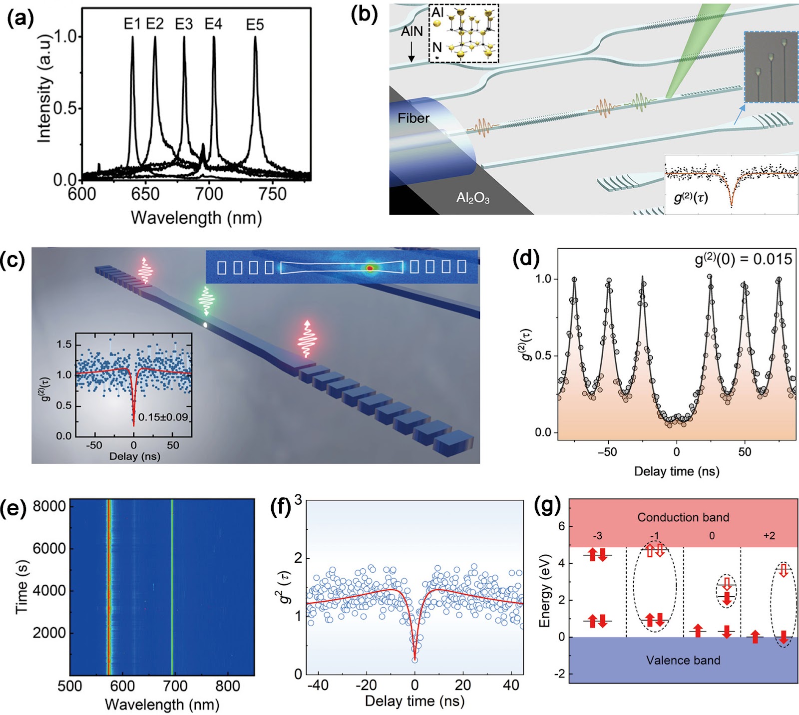
Overcoming photovoltage deficit via phenylthiourea derivatives for efficient printed perovskite solar cells with enhanced stability
Graphical Abstract
Original ResearchVol. 32, Issue 8 • pp. 100-112DOI: 10.1088/1674-4926/25080038Jan 15, 2025

A low-thermal-budget MOSFET-based reservoir computing for temporal data classification

Authors: Yanqing Li, Feixiong Wang, Heyi Huang, Yadong Zhang, Xiangpeng Liang, Shuang Liu, Jianshi Tang, Huaxiang Yin

Neuromorphic devices have garnered significant attention as potential building blocks for energy-efficient hardware systems owing to their capacity to emulate the computational efficiency of the brain. In this regard, reservoir computing (RC) framework, which leverages straightforward training methods and efficient temporal signal processing, has emerged as a promising scheme. While various physical reservoir devices, including ferroelectric, optoelectronic, and memristor-based systems, have been demonstrated, many still face challenges related to compatibility with mainstream complementary metal oxide semiconductor (CMOS) integration processes. This study introduced a silicon-based schottky barrier metal−oxide−semiconductor field effect transistor (SB-MOSFET), which was fabricated under low thermal budget and compatible with back-end-of-line (BEOL). The device demonstrated short-term memory characteristics, facilitated by the modulation of schottky barriers and charge trapping. Utilizing these characteristics, a RC system for temporal data processing was constructed, and its performance was validated in a 5 × 4 digital classification task, achieving an accuracy exceeding 98% after 50 training epochs. Furthermore, the system successfully processed temporal signal in waveform classification and prediction tasks using time-division multiplexing. Overall, the SB-MOSFET's high compatibility with CMOS technology provides substantial advantages for large-scale integration, enabling the development of energy-efficient reservoir computing hardware.

A low-thermal-budget MOSFET-based reservoir computing for temporal data classification
Graphical Abstract
Original ResearchVol. 32, Issue 9 • pp. 100-112DOI: 10.1088/1674-4926/25090008Jan 15, 2025

High-speed single-mode 850 nm vertical-cavity surface-emitting laser

Authors: Si-Cong Tian

A high-speed single-mode vertical-cavity surface-emitting laser (VCSEL) is one of the most important light sources for optical interconnects in data centers. Single-mode VCSEL can improve the transmission distance. In this letter, we demonstrate a single-mode 850 nm VCSEL with a bit rate of 60 Gb/s under NRZ modulation and 104 Gb/s under PAM4 modulation across a 100 m length of OM5 fiber, without the need for equalization or a filter. In addition, by using optical injection locking, the 3 dB bandwidth is enhanced to 68.5 GHz.

High-speed single-mode 850 nm vertical-cavity surface-emitting laser
Graphical Abstract
Original ResearchVol. 32, Issue 9 • pp. 100-112DOI: 10.1088/1674-4926/25090014Jan 15, 2025

Enhanced Low Dose Rate Sensitivity and Pre-Irradiation Elevated-Temperature Stress Effects in Bipolar Devices: Role of Hydrogen in the Passivation Layer

Authors: Shilong Gou, Wuying Ma, Zhibin Yao, Zujun Wang, Jiangkun Sheng, Yuanyuan Xue

Enhanced low dose rate sensitivity (ELDRS) experiments were carried out on four commercial bipolar integrated circuits at dose rates ranging from 0.002 to 50 rad(Si)/s. Additionally, pre-irradiation elevated-temperature stress (PETS) experiments were conducted on the same devices at temperatures of 250 and 400 °C. The results show that for some devices, the radiation degradation when irradiated at an ultra-low dose rate of 0.002 rad(Si)/s is more than three times greater than that at a common low dose rate of 0.01 rad(Si)/s. Moreover, the maximum enhancement factor of the PETS effects reaches 20.3. It was also discovered that for devices exhibiting PETS effects, the saturation dose rate of ELDRS is less than 0.01 rad(Si)/s. A comprehensive analysis of the composition of the passivation layers indicated that the type and concentration of hydrogen bonds in these layers are the main factors contributing to the experimental outcomes.

Enhanced Low Dose Rate Sensitivity and Pre-Irradiation Elevated-Temperature Stress Effects in Bipolar Devices: Role of Hydrogen in the Passivation Layer
Graphical Abstract
Original ResearchVol. 32, Issue 10 • pp. 100-112DOI: 10.1088/1674-4926/25100021Jan 15, 2025

Synergistic Performance and Yield Improvement of Embedded RRAM Product through Process Optimization in 40 nm CMOS Platform

Authors: Zhenchao Sui, Yanqing Wu, Zhichao Lv, Xing Zhang

To address the challenges of complexity, power consumption, and cost constraints in traditional display driver integrated circuits (DDICs) caused by external NOR Flash and SRAM, this work proposes an embedded resistive random-access memory (RRAM) integration solution based on a 40 nm high-voltage CMOS logic platform. Targeting the yield fluctuations and stability challenges during RRAM mass production, systematic process optimizations are implemented to achieve synergistic improvements in RRAM performance and yield. Through modifications to the film sputtering and pre-deposition treatment, the within-wafer resistance uniformity (RSU) of the oxygen-deficient layer (ODL) thin film is improved from 11% to 8%, while inter-wafer process stability variation reduces from 23% to below 6%. Consequently, the yield of 8 Mb RRAM embedded mass production products increases from 87% to 98.5%. In terms of device performance, the RRAM demonstrates a fast 4.8 ns read speed, exceptional read disturb immunity of 3 × 10^8 cycles at 95 °C, 10^3 write/erase endurance cycles for the 1 Mb cells, and data retention of 12.5 years at 125 °C. Post high-temperature operating life (HTOL) testing exhibits stable high/low resistance window. This study provides process optimization strategies and a reliability assurance framework for the mass production of highly integrated, low-power embedded RRAM display driver IC.

Synergistic Performance and Yield Improvement of Embedded RRAM Product through Process Optimization in 40 nm CMOS Platform
Graphical Abstract
Original ResearchVol. 32, Issue 10 • pp. 100-112DOI: 10.1088/1674-4926/25100007Jan 15, 2025

A Distributed Static Model of Capacitive MEMS Microwave Power Detection Chip

Authors: Ruifeng Li, Debo Wang

To improve the theoretical prediction accuracy of static mechanical quantities in MEMS cantilever beams for microwave power detection chips, a distributed static model is proposed based on the deflection equation. An analytical framework is established through the precise characterization of cantilever beam bending. The framework can accurately extract key electromechanical parameters, and the correlation between these parameters and geometric changes is systematically studied. Results show that the pull-in voltage increases with the gap but decreases with the length. The predicted pull-in voltage indicates a relative error of only 6.5% between the distributed static model and the simulation, which is significantly lower than that of the other two models. The overload power and sensitivity are also analyzed to facilitate performance trade-offs in chip design. The measured return loss varies between −66.46 and −10.56 dB over the 8−12 GHz frequency band, exhibiting a characteristic V-shaped trend. Moreover, the measured sensitivity of 66.5 fF/W closely matches the theoretical value of 69.3 fF/W, showing a relative error of 5.6%. These findings confirm that the distributed model outperforms the other two in terms of both accuracy and physical realism, thereby providing important reference for the design of microwave power detection chips.

A Distributed Static Model of Capacitive MEMS Microwave Power Detection Chip
Graphical Abstract
Original ResearchVol. 32, Issue 12 • pp. 100-112DOI: 10.1088/1674-4926/25120029Jan 15, 2025

PL spectra and PL dynamics of CsPbBr3 quantum dots in solution and film

Authors: Zhengda Dong, Dachuan Li, Pingyuan Yan, Chuanxiang Sheng

Temperature dependent photoluminescence (PL) and time-resolved PL (TRPL) of CsPbBr3 quantum dots (QDs) in solution and film are investigated. The electron−phonon coupling strength of quantum dots in solution is found two times larger than that of thin films. The averaged phonon energy involved in luminescence is also significantly higher than that of thin films, indicating that ligands’ phonons are involved in optical processes in solution but not in film. TRPL shows that the luminescence lifetime of the solution (22.5 ns) is longer than that of the thin film (5 ns) at room temperature, and both decrease abnormally with decreasing temperature, ascribing to the thermally activated trap states for PL, the further analysis shows that the trap energy levels in the thin film are deeper (~20 meV) compared to ~4 meV in solution. Our work proves that the morphology of organic ligands can regulate electron−phonon interactions and optoelectronic properties in CsPbBr3 QDs, providing fundamental insights into its photophysics.

PL spectra and PL dynamics of CsPbBr3 quantum dots in solution and film
Graphical Abstract
Original ResearchVol. 32, Issue 11 • pp. 100-112DOI: 10.1088/1674-4926/25110013Jan 15, 2025

Advancing Highly Efficient and Mechanically Resilient Flexible Perovskite-Silicon Tandem Solar Cells

Authors: Zhaoyang Han, Qi Jiang

Perovskite-silicon tandem solar cells, combining high power conversion efficiency (PCE) with cost-effectiveness, are a leading direction for next-generation photovoltaics. In two-terminal tandems, a crystalline silicon (c-Si) bottom cell is series-connected with a wide-bandgap (1.65–1.7 eV) perovskite top cell, leveraging complementary spectral absorption to enhance sunlight harvesting. Rigid perovskite/c-Si tandems have achieved certified PCEs up to 34.9%, exceeding the Shockley–Queisser limit for single junctions. However, flexible perovskite-silicon tandems have lagged due to the intrinsic rigidity of c-Si, interfacial delamination under bending, and processing challenges. Recent breakthroughs in Nature report significant progress. One study by Zhang, Liu, and colleagues from Soochow University and LONGi Green Energy Technology developed a dual-buffer layer strategy using dense and loose SnOx layers formed by modulating ALD purge time. The dense layer ensures efficient charge extraction, while the loose layer acts as a cushion to relieve mechanical stress from TCO sputtering and bending. This architecture achieved a certified efficiency of 33.4% on 1 cm² and 29.8% on a wafer-scale module (~260 cm²), with a power-to-weight ratio of 1.77 W/g and bendability to 15 mm radius. These advances demonstrate the potential of flexible perovskite-silicon tandems for aerospace, wearable, and IoT applications, addressing key challenges in efficiency, flexibility, and durability.

Advancing Highly Efficient and Mechanically Resilient Flexible Perovskite-Silicon Tandem Solar Cells
Graphical Abstract
Original ResearchVol. 32, Issue 11 • pp. 100-112DOI: 10.1088/1674-4926/25110003Jan 15, 2025

Evolution of Diamond Film Growth Modes under Varied Plasma Conditions: Insights from Optical Emission Spectroscopy

Authors: Pengfei Qu, Guangdi Zhou, Peng Jin, Xu Han, Zhanguo Wang

The synthesis of high-quality heteroepitaxial diamond films on iridium composite substrates is a critical step toward advancing diamond for electronic and optical applications. Microwave plasma chemical vapor deposition, combined with in situ optical emission spectroscopy, enables precise control over growth modes through plasma parameter tuning. In this study, we examine how methane concentration, microwave power, and gas pressure influence plasma species and, consequently, the growth modes of heteroepitaxial diamond by optical emission spectroscopy and scanning electron microscope. At low nucleation densities, increased methane concentrations promote the transition from faceted polyhedral to ballas structures, driven by elevated C2 radical concentrations in the plasma. Conversely, at higher nucleation densities, gas pressure, and substrate temperature dominate growth mode determination, leading to diverse morphologies, such as planar, polycrystalline, octahedral, and step-flow growth. These findings elucidate the interplay among plasma species, growth parameters, and growth mode, offering critical insights for optimizing growth conditions and preparing heteroepitaxial diamond films in a specific growth mode.

Evolution of Diamond Film Growth Modes under Varied Plasma Conditions: Insights from Optical Emission Spectroscopy
Graphical Abstract
Original ResearchVol. 32, Issue 11 • pp. 100-112DOI: 10.1088/1674-4926/25110004Jan 15, 2025

Realization of 193 nm DUV Laser through Direct Frequency Doubling with GaN-based UVA Laser Diode and ABF Crystal

Authors: Feng Liang, Fangfang Zhang, Jing Yang, Degang Zhao, Shilie Pan

The 193 nm deep-ultraviolet (DUV) laser is crucial for advanced semiconductor manufacturing, micro-nano material characterization, and biomedical analysis due to its high spatial resolution and short wavelength. Currently, ArF excimer gas lasers dominate DUV lithography, but alternative approaches based on infrared solid-state lasers suffer from complexity and low efficiency. Direct frequency doubling of long-wavelength ultraviolet (UVA) semiconductor lasers using DUV nonlinear optical crystals offers a promising alternative. However, practical implementation has been challenging due to limited availability of high-quality UVA laser diodes and DUV crystals with balanced properties. In this study, we demonstrate the first realization of a 193 nm DUV laser via direct frequency doubling of a GaN-based UVA laser diode using a high-quality fluorooxoborate crystal NH4B4O6F (ABF). Two UVA laser diodes emitting at 386 nm and 394 nm were used, generating 193 nm and 197 nm DUV emission, respectively. The experimental setup comprised a GaN-based UVA laser diode, an ABF crystal for frequency doubling, and a prism for spectral separation. Our results confirm the technical feasibility of this approach, opening a novel pathway toward compact, stable, and efficient 193 nm laser sources with substantial application potential in advanced semiconductor manufacturing, including DUV lithography monitoring, wafer inspection, and defect analysis.

Realization of 193 nm DUV Laser through Direct Frequency Doubling with GaN-based UVA Laser Diode and ABF Crystal
Graphical Abstract
Original ResearchVol. 32, Issue 12 • pp. 100-112DOI: 10.1088/1674-4926/25120027Jan 15, 2025

A 2 mm × 2 mm Battery-Free Neural Interface Achieving 72-Channel Wireless Simultaneous Recording by Dual Overlapped On-Chip Antennas

Authors: Yili Shen, Yunshan Zhang, Changgui Yang, Yuxuan Luo, Bo Zhao

Battery-free radio systems utilizing wireless power transfer (WPT) further facilitate the miniaturization of neural implants. However, simultaneous monitoring of multiple neuronal activities is required to obtain high-fidelity neural signals. Consequently, the integration of numerous channels on a single chip and the wireless transmission of massive multi-channel data pose significant challenges for implantable battery-free neural interfaces. This work introduces dual overlapped on-chip antennas to eliminate the need for a battery in the neural implants and enable high-data-rate backscatter for transmitting the massive data acquired simultaneously from 72 channels. Additionally, an orthogonal coding and sampling technique is employed to reduce both power consumption and area per channel. Fabricated in a 65 nm CMOS process, the proposed chip integrates 72 neural recording channels within a 2 mm × 2 mm area and achieves a backscatter data rate of 18 Mbps.

A 2 mm × 2 mm Battery-Free Neural Interface Achieving 72-Channel Wireless Simultaneous Recording by Dual Overlapped On-Chip Antennas
Graphical Abstract
Original ResearchVol. 32, Issue 12 • pp. 100-112DOI: 10.1088/1674-4926/25120014Jan 15, 2025

Electrohydrodynamic Inkjet Printing of Perovskite Quantum Dots for Color-Conversion Micro-LED Displays

Authors: LIN Chenyun, FAN Xiaotong, GU Yuxuan, CAI Siting, CHEN Zhong, WANG Shuli, LIN Yue

Electrohydrodynamic (EHD) inkjet printing has emerged as a powerful micro-/nanofabrication technique for high-resolution perovskite quantum dot (PeQD) color-conversion layers, offering precise control over pixel morphology, dimensions, and composition. This review systematically examines the mechanisms of cone-jet and electrostatic-attraction modes in EHD printing, highlighting recent advances in PeQD ink design, solvent and ligand engineering, and printing parameter optimization. Perovskite precursor and colloidal inks are discussed in detail, emphasizing strategies to enhance droplet ejection stability, suppress coffee-ring effects, and achieve uniform, high-luminescence pixels. Ligand exchange, dual-ligand passivation, and core−shell or polymer encapsulation are shown to effectively mitigate ion migration, surface defects, and environmental degradation, thereby improving photoluminescence efficiency and stability. Multi-channel and multi-nozzle EHD printing systems enable dynamic halide composition control and parallel RGB pixel deposition, facilitating ultrahigh-resolution patterning down to submicron feature sizes. Finally, the review highlights future directions, including synergistic PeQD material synthesis, advanced ink formulation, scalable high-throughput printing, and integration of PeQD color-conversion pixels into full-color micro-LED displays with minimal crosstalk and robust operational stability. These developments collectively demonstrate the immense potential of EHD inkjet printing for next-generation high-performance display technologies.
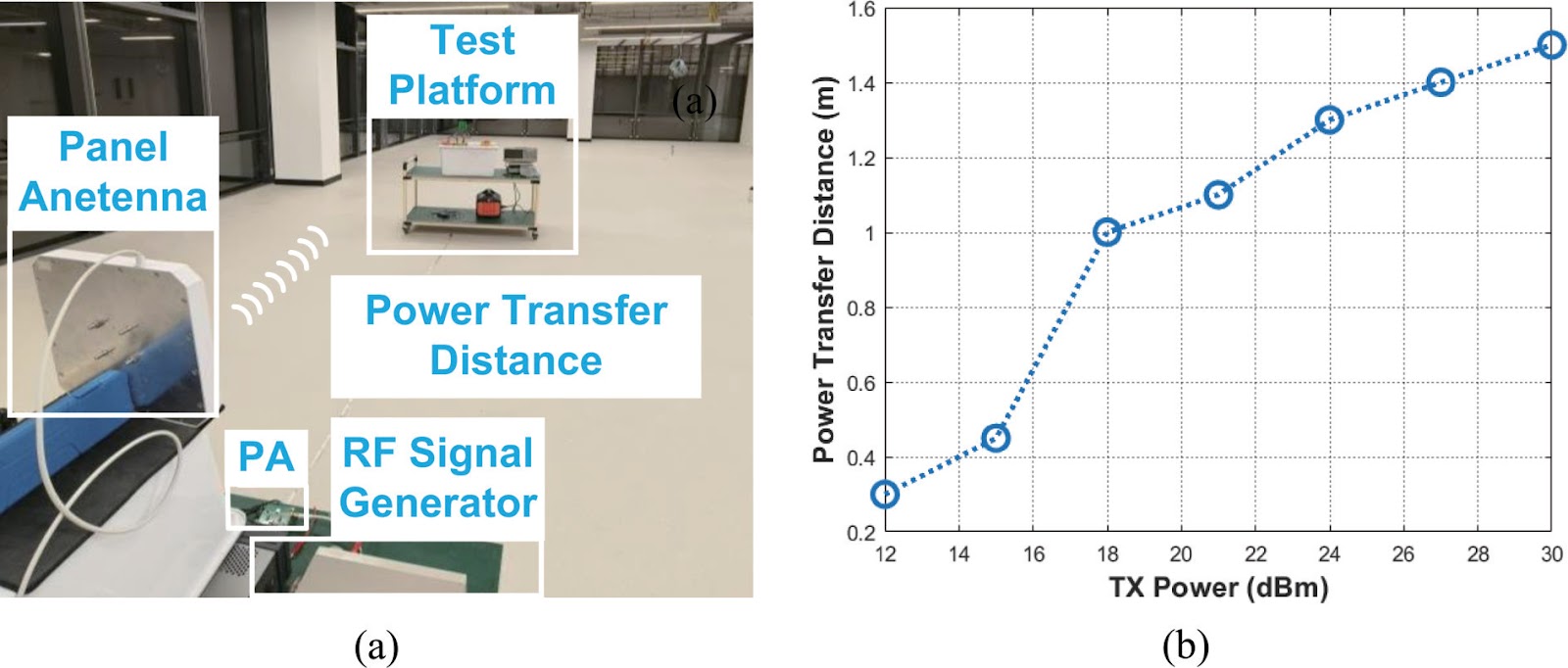
Electrohydrodynamic Inkjet Printing of Perovskite Quantum Dots for Color-Conversion Micro-LED Displays
Graphical Abstract
Original ResearchVol. 32, Issue 12 • pp. 100-112DOI: 10.1088/1674-4926/25120042Jan 15, 2025

Room-Temperature Electrically Injected GaN-Based Vertical-Cavity Surface-Emitting Laser with Conductive Nanoporous Distributed Bragg Reflector

Authors: Chuanjie Li, Meixin Feng, Jianping Liu, Aiqin Tian, Xuan Li, Wei Zhou, Rui Xi, Shuming Zhang, Qian Sun, Hui Yang

Vertical-cavity surface-emitting lasers (VCSELs) offer numerous advantages, including the ability to form two-dimensional arrays, low power consumption, and easy coupling, making them promising for visible-light communication, sensing, and micro-display applications. In GaAs-based VCSELs, conductive epitaxial semiconductor distributed Bragg reflectors (DBRs) enable straightforward vertical current injection. However, in GaN-based VCSELs, the lack of p-type conductive epitaxial DBRs has necessitated complex fabrication processes, such as flip-chip bonding and substrate thinning, which increase thermal resistance and reduce yield. In this work, we demonstrate a room-temperature electrically injected GaN-based VCSEL employing a conductive nanoporous (NP) GaN DBR. The NP-GaN DBR, fabricated by electrochemical etching of highly Si-doped n+-GaN layers, exhibits a high reflectivity of 99.9% with a stopband width of about 35 nm, while retaining excellent electrical conductivity. The device structure incorporates a 10λ cavity for enhanced lateral heat dissipation, a 10-μm-diameter current aperture, and a top dielectric DBR with reduced reflectivity (99.2%) to facilitate top emission. The vertical series resistance through the NP-GaN DBR is approximately 4.5 Ω, significantly lower than that of AlInN/GaN DBRs (>60 Ω), demonstrating the superior electrical performance of the NP-GaN DBR. This work presents a promising approach for achieving high-performance GaN-based VCSELs with simplified fabrication and improved thermal management, paving the way for their integration into high-density display and communication systems.
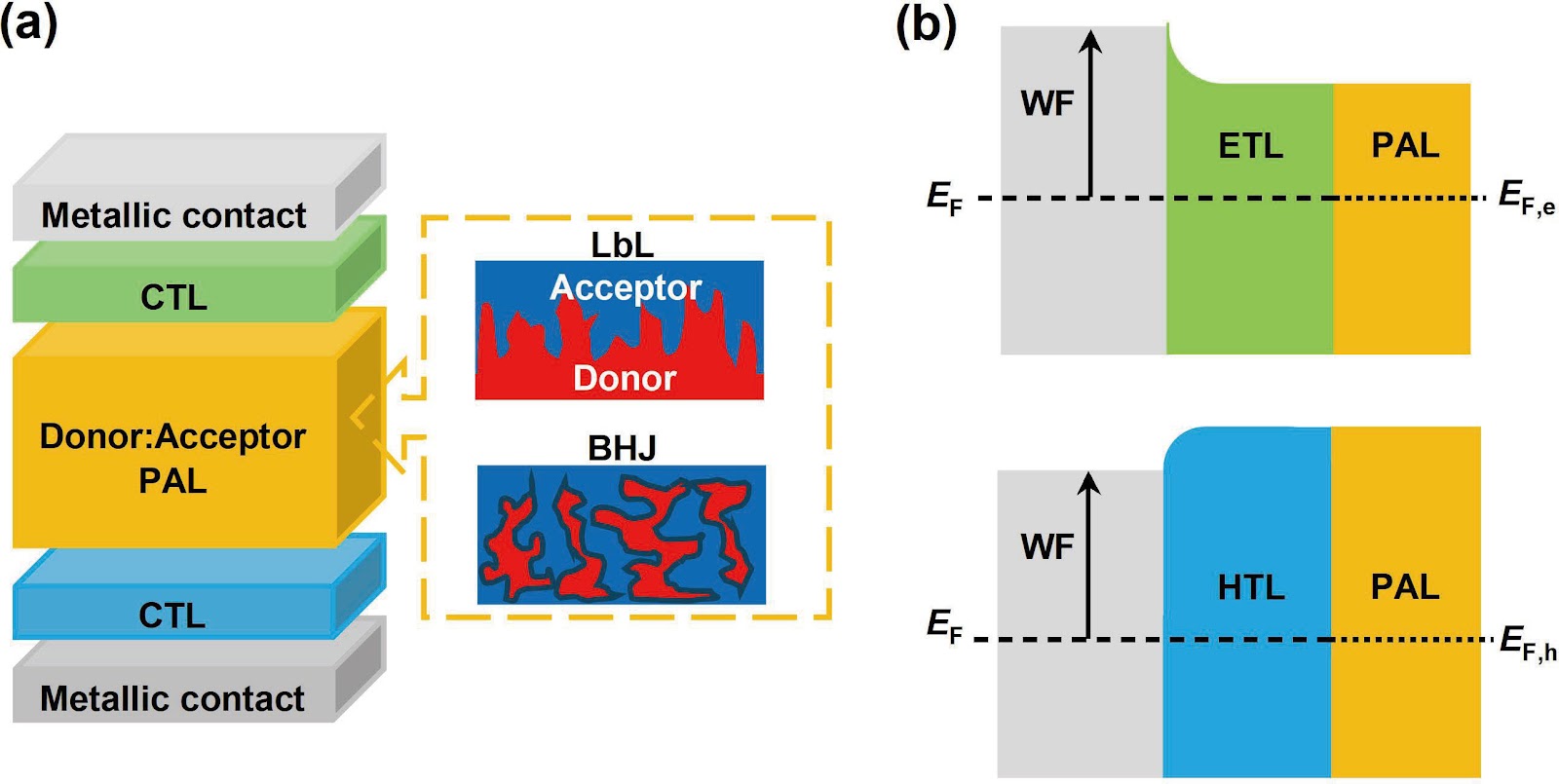
Room-Temperature Electrically Injected GaN-Based Vertical-Cavity Surface-Emitting Laser with Conductive Nanoporous Distributed Bragg Reflector
Graphical Abstract
Original ResearchVol. 32, Issue 12 • pp. 100-112DOI: 10.1088/1674-4926/25120050Jan 15, 2025

Electrochromic Retina E-Paper: Defining the Ultimate Display at the Human Vision Limit

Authors: Tongqing Zhou, Jianmin Li, Shujuan Liu, Qiang Zhao

In an era dominated by visual information, the display interface serves as a critical gateway between the human and digital worlds. The relentless pursuit of visual immersion has driven display technology from cinema screens to smartphones and now to virtual and augmented reality (VR/AR) headsets, progressively moving closer to the human eye. This evolution places unprecedented demands on pixel density, power efficiency, and form factor, pushing up against fundamental physical and physiological limits. The core challenge lies in creating displays that, when viewed at close proximity, offer a seamless, high-fidelity visual experience indistinguishable from reality—a goal often conceptualized as the 'retina display', where the pixel density matches or exceeds the resolving power of the human eye. However, as pixel sizes shrink into the sub-micrometer regime, conventional emissive technologies like organic light-emitting diodes (OLEDs) and micro-light-emitting diodes (micro-LEDs) face insurmountable hurdles: diminished emission intensity, non-uniformity, severe colour cross-talk, and rapidly increasing fabrication complexity. Even the most advanced micro-LED demonstrations struggle to achieve the required pixel densities across large fields of view without significant performance trade-offs. Conversely, reflective displays, or electronic paper (E-paper), which leverage ambient light for visibility, inherently avoid the luminosity and efficiency issues of emissive displays. Their optical contrast is governed by material properties at the nanoscale, remaining theoretically unaffected by pixel size reduction. Yet, established reflective technologies, such as electrophoretic displays (e.g., those in e-readers), have been hamstrung by slow refresh rates (seconds), limited colour gamuts, and resolutions typically below 1000 pixels per inch (PPI), confining them largely to static text and image applications. While optical metasurfaces have demonstrated astonishing static resolutions exceeding 10 000 PPI, they have largely remained just that—static—lacking the dynamic tunability essential for video and interactive content. Previous attempts to create dynamic reflective displays using hybrid nanomaterials have improved colour and speed but failed to break the micron-scale pixel barrier, leaving the holy grail of a high-resolution, video-rate, low-power reflective display tantalizingly out of reach. Now, writing in Nature, Santosa et al. achieve a retina E-paper that not only surmounts these historical limitations but also redefines the possibilities for ultra-high-resolution displays, based on traditional electrochromic (EC) technology. By demonstrating electrically tunable pixels down to ~560 nm in size (>25 000 PPI), full-colour video capability (>25 Hz), high reflectance (~80%), and remarkably low energy consumption (0.5–1.7 mW∙cm–2), they present a paradigm shift from light-emitting to intelligently light-modulating displays at the nanoscale.
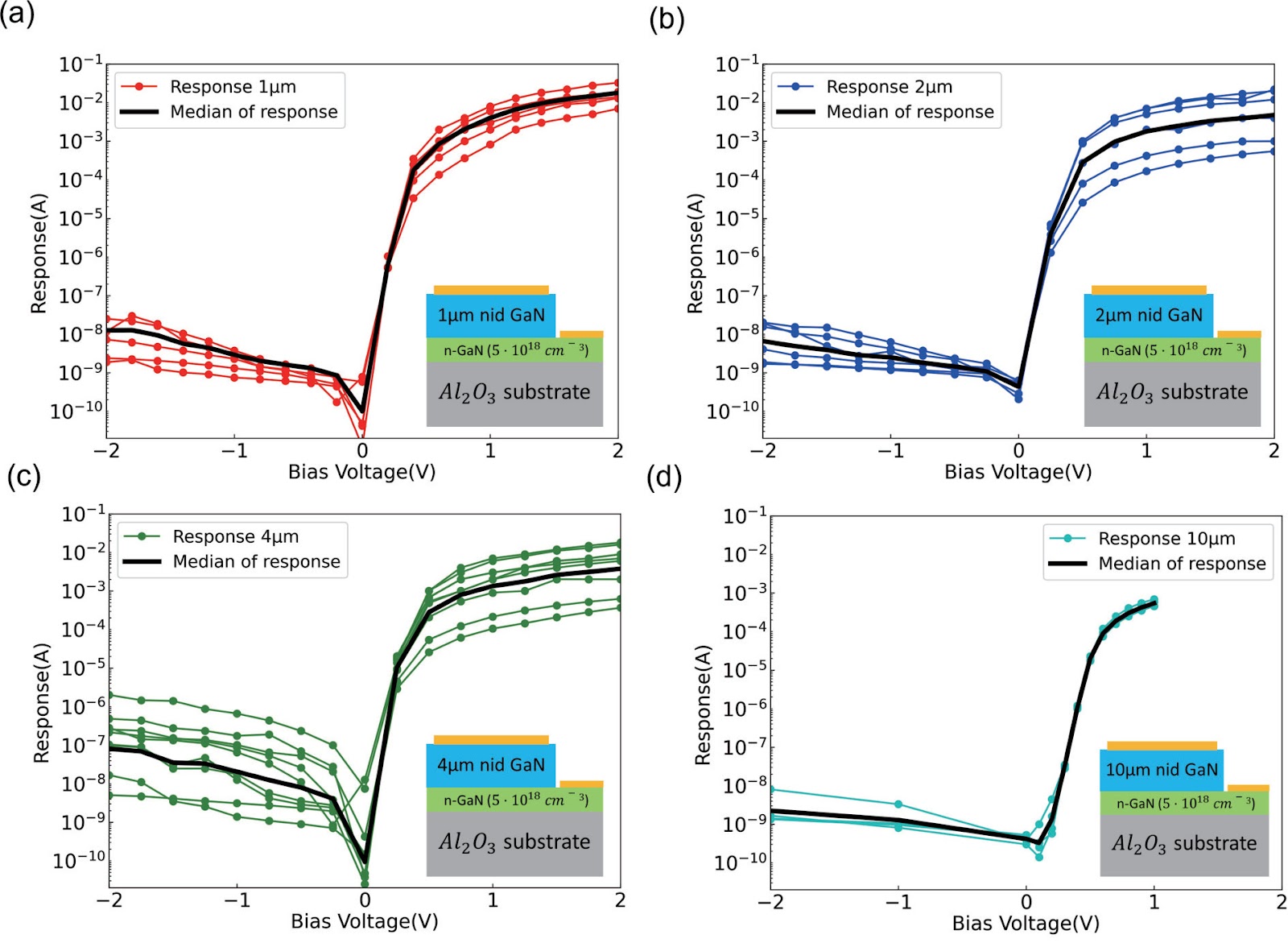
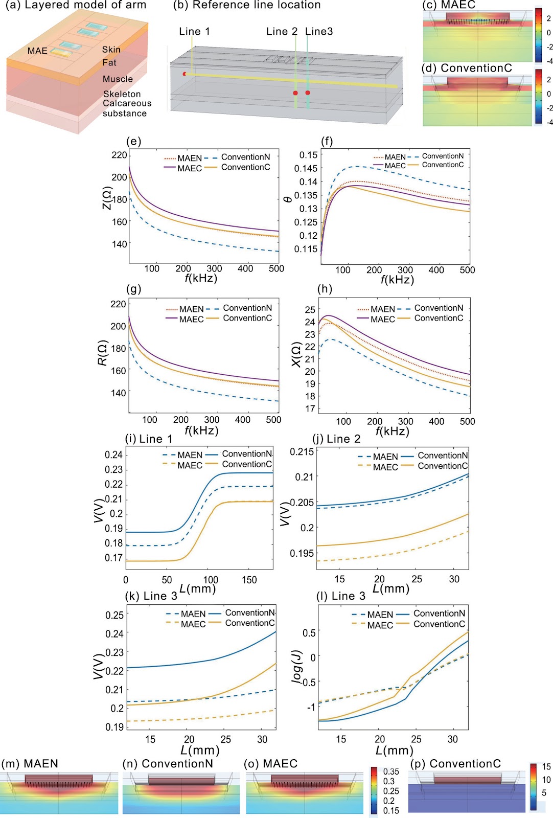

Electrochromic Retina E-Paper: Defining the Ultimate Display at the Human Vision Limit
Graphical Abstract
Original ResearchVol. 32, Issue 12 • pp. 100-112DOI: 10.1088/1674-4926/24120040Jan 15, 2024

Diverse methods and practical aspects in controlling single semiconductor qubits: a review

Authors: Jia-Ao Peng, Chu-Dan Qiu, Wen-Long Ma, Jun-Wei Luo

Quantum control allows a wide range of quantum operations employed in molecular physics, nuclear magnetic resonance and quantum information processing. Thanks to the existing microelectronics industry, semiconducting qubits, where quantum information is encoded in spin or charge degree freedom of electrons or nuclei in semiconductor quantum dots, constitute a highly competitive candidate for scalable solid-state quantum technologies. In quantum information processing, advanced control techniques are needed to realize quantum manipulations with both high precision and noise resilience. In this review, we first introduce the basics of various widely-used control methods, including resonant excitation, adabatic passage, shortcuts to adiabaticity, composite pulses, and quantum optimal control. Then we review the practical aspects in applying these methods to realize accurate and robust quantum gates for single semiconductor qubits, such as Loss–DiVincenzo spin qubit, spinglet-triplet qubit, exchange-only qubit and charge qubit.

Diverse methods and practical aspects in controlling single semiconductor qubits: a review
Graphical Abstract
Original ResearchVol. 32, Issue 12 • pp. 100-112DOI: 10.1088/1674-4926/24120034Jan 15, 2024

A 1.25 μW/ch TDM-based analog front-end using a charge-sharing multiplexer for bio-potential recording

Authors: Yifan Huang, Jing Wang, Lin Cheng

This paper presents the design of a low-power multi-channel analog front-end (AFE) for bio-potential recording. By using time division multiplexing (TDM), a successive approximation register analog-to-digital converter (SAR ADC) is shared among all 20 channels. A charge-sharing multiplexer (MUX) is proposed to transmit the output signals from the respective channels to the ADC. By separately pre-sampling the output of each channel, the sampling time of each channel is greatly extended and additional active buffers are avoided. The AFE is fabricated in a 65-nm CMOS process, and the whole system consumes 28.2 μW under 1 V supply. Each analog acquisition channel consumes 1.25 μW and occupies a chip area of 0.14 mm2. Measurement results show that the AFE achieves an input referred noise of 1.8 μV∙rms in a 350 Hz bandwidth and a noise efficiency factor (NEF) of 4.1. The 12-bit SAR ADC achieves an ENOB of 9.8 bit operating at 25 kS/s. The AFE is experimented on real-world applications by measuring human ECG and a clear ECG waveform is captured.

A 1.25 μW/ch TDM-based analog front-end using a charge-sharing multiplexer for bio-potential recording
Graphical Abstract
Original ResearchVol. 32, Issue 12 • pp. 100-112DOI: 10.1088/1674-4926/24120026Jan 15, 2024

Minimizing tin (Ⅱ) oxidation using ethylhydrazine oxalate for high-performance all-perovskite tandem solar cells

Authors: Jianhua Zhang, Xufeng Liao, Weisheng Li, Yutian Tian, Qinyang Huang, Yitong Ji, Guotang Hu, Qingguo Du, Wenchao Huang, Donghoe Kim, Yi-Bing Cheng, Jinhui Tong

All-perovskite tandem solar cells (ATSCs) have the potential to surpass the Shockley−Queisser efficiency limit of conventional single-junction devices. However, the performance and stability of mixed tin–lead (Sn–Pb) perovskite solar cells (PSCs), which are crucial components of ATSCs, are much lower than those of lead-based perovskites. The primary challenges include the high crystallization rate of perovskite materials and the susceptibility of Sn2+ oxidation, which leads to rough morphology and unfavorable p-type self-doping. To address these issues, we introduced ethylhydrazine oxalate (EDO) at the perovskite interface, which effectively inhibits the oxidation of Sn2+ and simultaneously enhances the crystallinity of the perovskite. Consequently, the EDO-modified mixed tin−lead PSCs reached a power conversion efficiency (PCE) of 21.96% with high reproducibility. We further achieved a 27.58% efficient ATSCs by using EDO as interfacial passivator in the Sn−Pb PSCs.

Minimizing tin (Ⅱ) oxidation using ethylhydrazine oxalate for high-performance all-perovskite tandem solar cells
Graphical Abstract
Original ResearchVol. 32, Issue 12 • pp. 100-112DOI: 10.1088/1674-4926/24120014Jan 15, 2024

Mid-wavelength infrared planar junction photodetector based on InAs/GaSb Type-Ⅱ superlattices

Authors: ZHANG Shihao, HAO Hongyue, ZHANG Ye, WANG Shuo, ZHANG Xiangyu, XIE Ruoyu, YAO Lingze, CHANG Faran, SHAN Yifan, LIU Haofeng, WANG Guowei, WU Donghai, JIANG Dongwei, XU Yingqiang, NIU Zhichuan, DONG Wenjing

In this paper, a planar junction mid-wavelength infrared (MWIR) photodetector based on an InAs/GaSb type-Ⅱ superlattices (T2SLs) is reported. The Intrinsic-πMN superlattices was grown by the molecular beam epitaxy (MBE), followed with a ZnS layer grown by the chemical vapor deposition (CVD). The p-type contact layer was constructed by thermal diffusion in the undoped superlattices. The Zinc atom was successfully realised into the superlattice and a PπMN T2SL structure was constructed. Furthermore, the effects of different diffusion temperatures on the dark current performance of the devices were researched. The 50% cut-off wavelength of the photodetector is 5.26 μm at 77 K with 0 V bias. The minimum dark current density is 8.67 × 10⁻⁵ A/cm2 and the maximum quantum efficiency of 42.5%, and the maximum detectivity reaches 3.90 × 1010 cm·Hz1/2/W at 77 K. The 640 × 512 focal plane arrays (FPA) based on the planner junction were fabricated afterwards. The FPA achieves a noise equivalent temperature difference (NETD) of 539 mK.

Mid-wavelength infrared planar junction photodetector based on InAs/GaSb Type-Ⅱ superlattices
Graphical Abstract
Original ResearchVol. 32, Issue 12 • pp. 100-112DOI: 10.1088/1674-4926/24120018Jan 15, 2024

Size matters: quantum confinement-driven dynamics in CsPbI3 quantum dot light-emitting diodes

Authors: LI Shuo, YIN Wenxu, ZHENG Weitao, ZHANG Xiaoyu

The quantum confinement effect fundamentally alters the optical and electronic properties of quantum dots (QDs), making them versatile building blocks for next-generation light-emitting diodes (LEDs). This study investigates how quantum confinement governs the charge transport, exciton dynamics, and emission efficiency in QD-LEDs, using CsPbI3 QDs as a model system. By systematically varying QD sizes, we reveal size-dependent trade-offs in LED performance, such as enhanced efficiency for smaller QDs but increased brightness and stability for larger QDs under high current densities. Our findings offer critical insights into the design of high-performance QD-LEDs, paving the way for scalable and energy-efficient optoelectronic devices.

Size matters: quantum confinement-driven dynamics in CsPbI3 quantum dot light-emitting diodes
Graphical Abstract
Original ResearchVol. 32, Issue 12 • pp. 100-112DOI: 10.1088/1674-4926/24121701Jan 15, 2024

Preface to Special Issue on Flexible and Smart Electronics for Sensors 4.0

Authors: Zhuoran Wang, Yang Li, Qilin Hua

The evolution of information technology has propelled the advancement of sensors into a new era, referred to as Sensors 4.0. This era is characterized by the integration of key technological developments, including the internet of things (IoT), Industry 4.0, big data, artificial intelligence (AI), robotics, and digital health. These innovations necessitate that sensors become increasingly interconnected and intelligent. The concept of 'everything is connected' demands that sensors undertake a broader and more complex range of tasks, a challenge that conventional, bulky devices are ill-equipped to address. In addition to pursuing improvements in sensitivity and bandwidth, as seen in the 'more Moore' approach—focused on extracting the last few nanometers from process nodes—the paradigm of 'more than and beyond Moore' presents new opportunities in the Sensors 4.0 era. A key breakthrough in this context is the development of devices with flexibility, which introduces a new mechanical dimension to the conventional sensor form factor. This innovation lays the foundation for next-generation distributed sensory applications that are deformable, miniaturized, and lightweight. Furthermore, recent advancements in multimodal, biomimetic, AI-enhanced, and all-in-one sensing materials and devices are pushing the boundaries of smart electronics. These developments aim to achieve minimal power consumption while enhancing overall functionality. Consequently, flexibility and intelligence have emerged as two critical features driving the development of novel and compelling electronic sensory applications in Sensors 4.0, thus lead to the organization of our Special Issue at the very beginning of 2025 that collects critical research progress and strategic reviews across multidisciplinary subjects of flexible and smart electronics. Specifically, this Special Issue features six research articles and ten review articles contributed by leading experts in the field, categorized into three themes: 1) Sensory applications for light, gas, and temperature measurement, focusing on the fabrication and design of flexible platforms; 2) neuromorphic electronic devices that integrate sensing, memory, and computation to develop next-generation parallel and low-power sensory systems; 3) integrated and multimodal sensory systems for IoT applications in areas such as biology and healthcare.

Preface to Special Issue on Flexible and Smart Electronics for Sensors 4.0
Graphical Abstract