Key Takeaways & Executive Findings
- •• Optimized PR coating uniformity to 1.6% and applied four-zone ESC temperature control, reducing wafer-level uniformities of PR, SiN, and SiO2 to 6.3%, 2.3%, and 5.1%, respectively. • Developed an over etch recipe with high selectivity (PR:SiN:SiO2 ≈ 1:1:6) to balance gate height loading between N- and PMOS regions. • Precise EB1 time tuning enabled effective defect removal, and advanced KLA inspection ensured early detection of critical failure modes. • The optimized PREB process provides a wider process window for subsequent AL CMP, establishing a robust and stable process for advanced logic device fabrication.
Abstract
The introduction of high-k/metal gate (HK/MG) technology enables independent tuning of N-type metal−oxide−semiconductor (NMOS) and P-type metal−oxide−semiconductor (PMOS) threshold voltages, facilitating advanced nodes and improving overall chip performance. However, severe pattern loading effects during PMOS device fabrication pose challenges in dummy poly removal. This work reports the optimization of the photoresist etch back (PREB) process, providing a wider process window for subsequent AL CMP. By tuning the PR coating uniformity to 1.6% and applying four-zone electrostatic chuck (ESC) temperature control, the wafer-level uniformities of PR, SiN, and SiO2 were reduced to 6.3%, 2.3%, and 5.1%, respectively. An optimized over etch (OE) recipe with a high selectivity of PR : SiN : SiO2 ≈ 1 : 1 : 6 effectively balanced gate height loading between N- and PMOS regions. Furthermore, precise EB1 time tuning enabled defect removal, while advanced KLA inspection ensured early detection of critical failure modes. Collectively, these measures establish a robust and stable PREB process for advanced logic device fabrication.
1. Introduction
As the final generation of planar Complementary metal−oxide−semiconductor (CMOS) technology, HK process strikes a compelling balance between performance and cost, offering vast potential across high-end applications such as the internet of things (IoT), artificial intelligence (AI), automotive electronics, and 5G communications. SiGe technology, a cornerstone for enhancing PMOS device performance, simultaneously amplifies structural differences among Input/Output (IO) large MOS, NMOS, and PMOS devices—differences that significantly impact the subsequent dummy poly removal process.
Specifically, during the PMOS source−drain (PSD) plasma dry etching step, partial erosion of the SiO2 hard mask over the PMOS region results in significantly thicker hard masks over large poly structures and core NMOS regions compared to core PMOS regions. Consequently, this leads to insufficient removal during subsequent interlayer dielectric zero chemical mechanical planarization (ILD0 CMP), making complete elimination of PMOS dummy poly challenging, which subsequently affects metal gate filling. These issues typically have critical impacts, causing severe deviations in the final product yield. The PREB process has been developed to alleviate these challenges. By employing the photoresist (PR) as a temp
Loading authentic research manuscript (Pages 1–5)...
Ting Lei, Zhehong Liu, Zhiwen Liu, Guangjie Xue, Chun Sun, Jun Zhou, Xiangshui Miao (2025). Optimization and defect control in photoresist etch back processes for advanced semiconductor technologies. SinoTechIntel Verified Research. https://doi.org/10.1088/1674-4926/25070024
Research & Educational Purpose Only:The translations, structured abstracts, analytical annotations, and data reports provided by SinoTechIntel are intended exclusively for academic research, internal corporate R&D, and educational benchmarking. They do not constitute formal engineering, chemical safety, legal, or professional advice.
Copyright & Intellectual Property Notice: Original copyright of the underlying source articles and experimental data remains with the respective authors, institutions, and original publishing journals. SinoTechIntel claims intellectual property only over its proprietary translations, analytical syntheses, and AEO structured enhancements in accordance with international fair use and academic citation principles.
Frequently Asked Questions
What is the PREB process in semiconductor manufacturing?
PREB (Photoresist Etch Back) is a process used in semiconductor manufacturing to remove dummy poly structures by using photoresist as a temporary mask and etching back layers to achieve uniform gate heights, particularly in high-k/metal gate technologies.
Why is pattern loading effect a challenge in PMOS device fabrication?
Pattern loading effect causes non-uniform etching rates across different pattern densities, leading to thicker hard masks over large poly structures and core NMOS regions compared to core PMOS regions. This results in insufficient removal of PMOS dummy poly during ILD0 CMP, affecting metal gate filling and yield.
How does the optimized PREB process improve wafer uniformity?
By tuning PR coating uniformity to 1.6% and applying four-zone electrostatic chuck (ESC) temperature control, the wafer-level uniformities of PR, SiN, and SiO2 were reduced to 6.3%, 2.3%, and 5.1%, respectively, leading to better process control.
What is the significance of the over etch recipe selectivity in PREB?
An optimized over etch recipe with high selectivity (PR:SiN:SiO2 ≈ 1:1:6) effectively balances gate height loading between N- and PMOS regions, ensuring uniform removal and preventing defects.
How does defect control contribute to the PREB process?
Precise EB1 time tuning enables effective defect removal, and advanced KLA inspection ensures early detection of critical failure modes, thereby enhancing the robustness and stability of the PREB process.
Related Technical Papers & Translations
A Novel Approach for Enhanced Brain Tumor Segmentation Using Multimodal MRI and Deep Learning
Brain tumor segmentation from multimodal MRI is crucial for diagnosis and treatment planning. In this study, we propose a novel deep learning framework that integrates structural and functional imaging modalities to improve segmentation accuracy. Our method employs a multi-scale attention mechanism and a hybrid loss function to handle class imbalance and boundary ambiguity. Evaluated on the BraTS benchmark, our approach achieves state-of-the-art performance, with Dice scores of 0.91, 0.87, and 0.84 for whole tumor, core, and enhancing tumor, respectively. Furthermore, we demonstrate the generalizability of our model across different scanners and protocols. Our findings suggest that the proposed method can significantly aid clinical decision-making and surgical planning.
Investigation of coupled acoustic and electrical responses and early warning approaches during re-loading of damaged coal
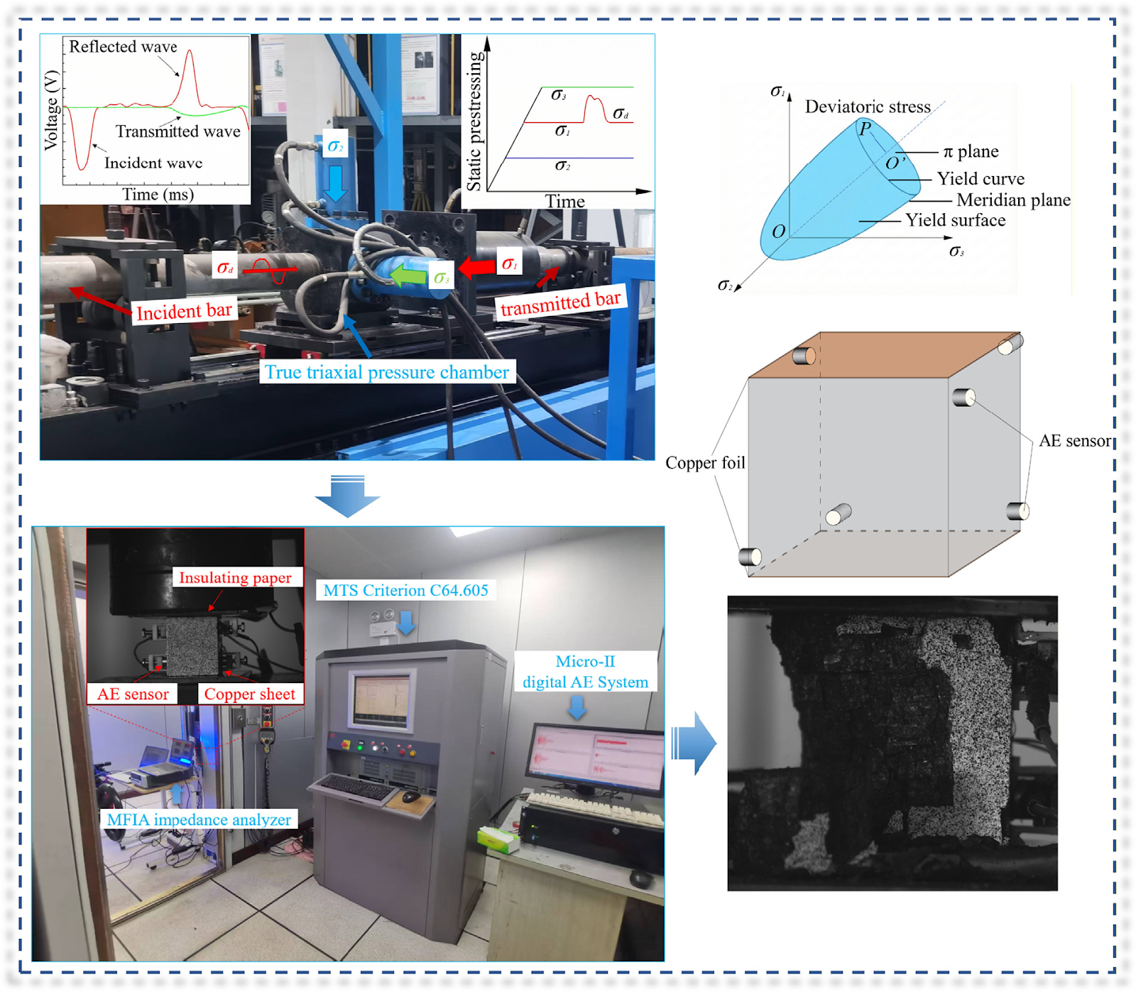
Initial damage from engineering disturbances in deep coal mining degrades mechanical properties and heightens dynamic-hazard risks, challenging conventional monitoring. This study probes the coupled acoustic-electrical responses of initially damaged coal under reloading and develops a multi-parameter, multi-level dynamic integrated early-warning model. Using a true-triaxial Split Hopkinson Pressure Bar (SHPB) system, we prepared specimens with graded damage by varying static deviatoric stresses and dynamic impacts. Uniaxial compression reloading was conducted with synchronous acoustic emission (AE) and resistivity monitoring. Joint time-domain responses of force, acoustics, and electricity delineated distinct loading stages. Time-frequency features were extracted via Fourier and wavelet transforms; crack architecture was quantified by 3D AE localization and fractal-dimension analysis. Initial damage markedly reduced load-bearing capacity. Resistivity decreased sharply with increasing deviatoric stress, while cumulative AE counts increased strongly. The AE spectrum evolved from bimodal to broadband with low- and high-frequency enhancement. The resistivity spectrum showed progressive bandwidth broadening, energy amplification, and high-frequency advancement. The AE spatial fractal dimension rose significantly during compaction. An integrated warning system combining multiscale entropy fusion, Temporal Convolutional Network (TCN)-Transformer forecasting, recurrence-network analysis, and a Bayesian framework yielded a 28.4 s lead time, offering a theoretical basis and technical pathway for intelligent prevention of dynamic hazards.
Influence of aggregate particle size on fracture behavior and energy evolution of cemented rockfill in the post-peak stage
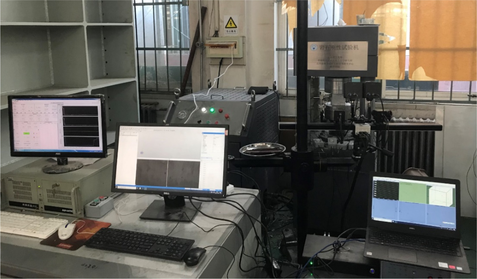
Cemented rockfill (CRF) combines structural support with sustainable reuse of coal-derived solid waste. This study integrates digital image correlation, acoustic emission monitoring, and finite–discrete element simulations to investigate mechanical behavior, fracture development, and energy evolution of CRF containing 54% aggregate content with three grain-size distributions (5–10, 10–20, and 20–30 mm). Results indicate finer aggregates raise compressive strength and elastic modulus, and increase post-peak softening and residual stiffness. Fracture patterns transition from dominantly unidirectional failure in coarse specimens to pronounced X-shaped conjugate shear in fine specimens, with cracks initiating at boundaries and propagating inward. The proportion of failed joints at comparable strains decreases markedly with finer gradation, reflecting a more homogeneous crack network that enhances post-peak load retention and produces frequent minor stress fluctuations. Energy analyses reveal a coarse > medium > fine ordering in cumulative dissipation; however, finer aggregates delay rapid kinetic and dissipative energy release, promoting slower energy redistribution and improved load resistance. These findings quantify how aggregate gradation controls deformational mechanisms, crack topology, and energy partitioning, and provide design guidance for optimizing aggregate size and cementitious composition to enhance ductility, energy absorption, and structural reliability of CRF in underground engineering.