SinoTechIntel Academic Portal
Semiconductors & Electronic MaterialsStrategic Intelligence Pillar

Wide-Bandgap Semiconductors: 8-Inch SiC Wafers, GaN Power HEMT & Diamond Substrates

Authoritative reporting on Chinese crystal growth, planar epitaxy, and trench-gate SiC MOSFET fabrication for EV traction inverters and 5G/6G RF arrays.

Primary Focus: Gallium Nitride & Silicon CarbideCurated Papers: 24 Verified StudiesDomain Authority: SinoTechIntel

State-of-the-Art Executive Brief & Commercialization Roadmap

China is accelerating capital expenditure and academic research into third-generation (wide-bandgap) semiconductors to bypass advanced lithography restrictions. Spearheaded by Shandong University, CAS Institute of Semiconductors, and SICC, Chinese fabricators have successfully transitioned from 6-inch to 8-inch conductive silicon carbide (SiC) boules with defect dislocation densities below 10^3 cm^-2. In Gallium Nitride (GaN), GaN-on-Silicon and GaN-on-Diamond high-electron-mobility transistors (HEMT) have reached commercial mass production for 800V automotive charging architectures and phased-array radar transceivers, delivering breakdown voltages exceeding 1,200V with sub-milli-ohm on-resistance.

Core Technical Benchmarks & Performance Thresholds

SiC Wafer Diameter
8-inch (200 mm)
Commercial pilot lines at SICC and TankeBlue
Basal Plane Dislocation (BPD)
< 100 cm^-2
Low-defect physical vapor transport (PVT) growth
GaN HEMT Breakdown Voltage
> 1,200 V
Lateral and quasi-vertical device architectures
Thermal Conductivity (GaN-on-Diamond)
> 1,500 W/m·K
Interface engineering with ultra-thin SiNx

Lead Research Institutions & Enterprise Innovators

🏛️ CAS Institute of Semiconductors (Beijing)🏛️ Shandong University (State Key Lab of Crystal Materials)🏛️ Xidian University (Wired & Wireless Microelectronics Lab)🏛️ SICC Co., Ltd.🏛️ San’an Optoelectronics

Verified Chinese Research Papers in Gallium Nitride & Silicon Carbide

24 Studies Indexed
Research PaperYear: 2026
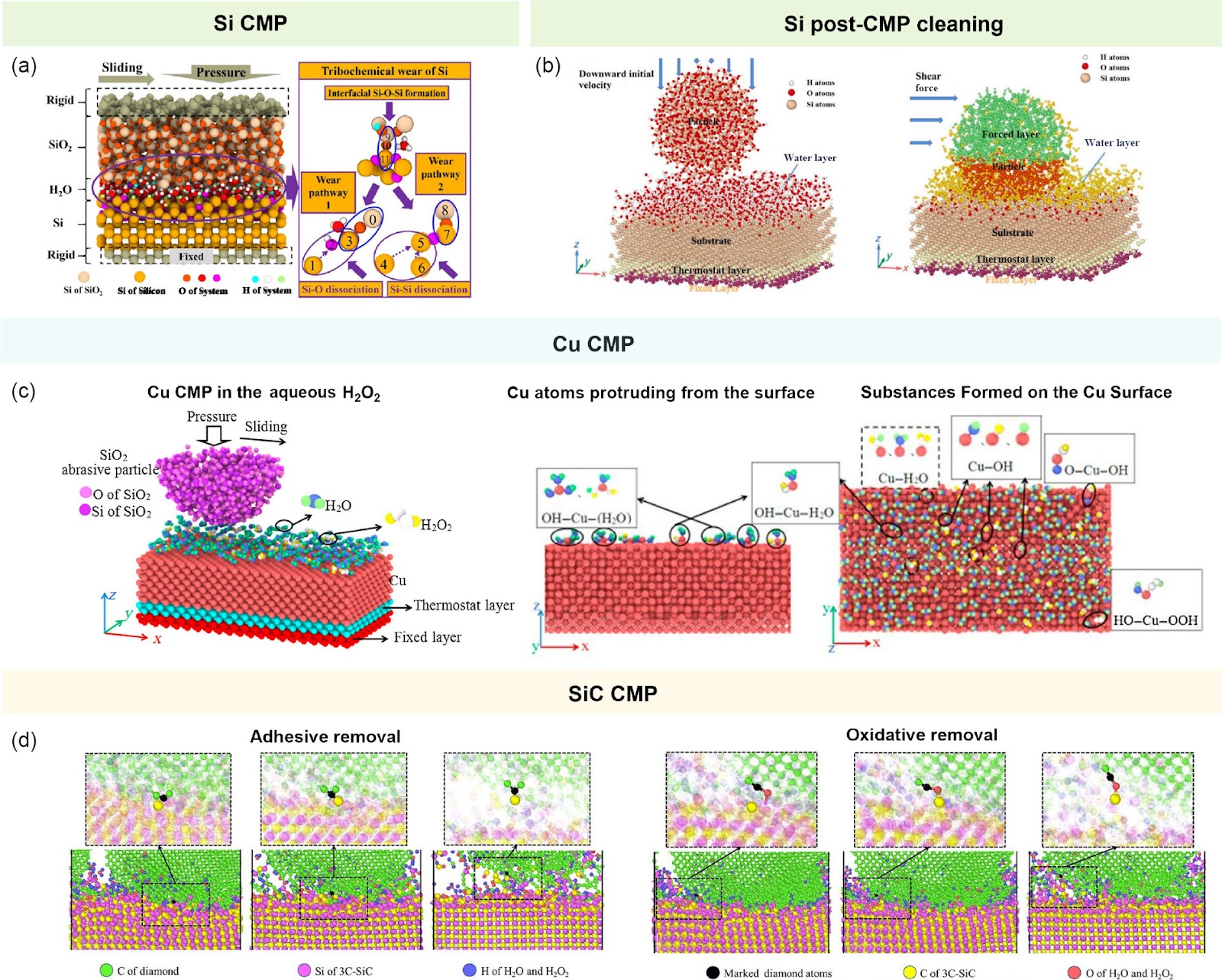
Molecular Dynamics Simulations Addressing Atomic-Scale Core Issues in Chemical Mechanical Polishing and Post-CMP Cleaning: A Concise Review

Molecular Dynamics Simulations Addressing Atomic-Scale Core Issues in Chemical Mechanical Polishing and Post-CMP Cleaning: A Concise Review

Chemical mechanical polishing (CMP) and post-CMP cleaning are critical steps in semiconductor manufacturing, requiring atomic-scale flatness and complete removal of contaminants. This review examines the use of molecular dynamics (MD) simulations to elucidate atomic-scale mechanisms underlying these processes, focusing on four major MD methodologies: classical MD, reactive force field MD (ReaxFF), tight-binding quantum chemical MD (TB-QC MD), and ab initio MD (AIMD). Classical MD provides a foundation for simulating large-scale systems but lacks accuracy for modeling chemical reactions. ReaxFF allows real-time bond breaking and formation simulations during CMP. TB-QC MD combines quantum accuracy with classical efficiency, enabling exploration of chemical reaction effects on friction and material removal. AIMD directly calculates atomic interactions for precise depictions of chemical processes, albeit with high computational cost. MD simulations act as a 'computational microscope', enhancing CMP and postcleaning processes by quantifying interactions, material removal pathways, and contaminant desorption. Future research should address multiscale modeling challenges, improve AIMD efficiency, and develop accurate potential functions to propel semiconductor manufacturing toward greater precision and efficiency.
Examine Data & PDF
Research PaperYear: 2026
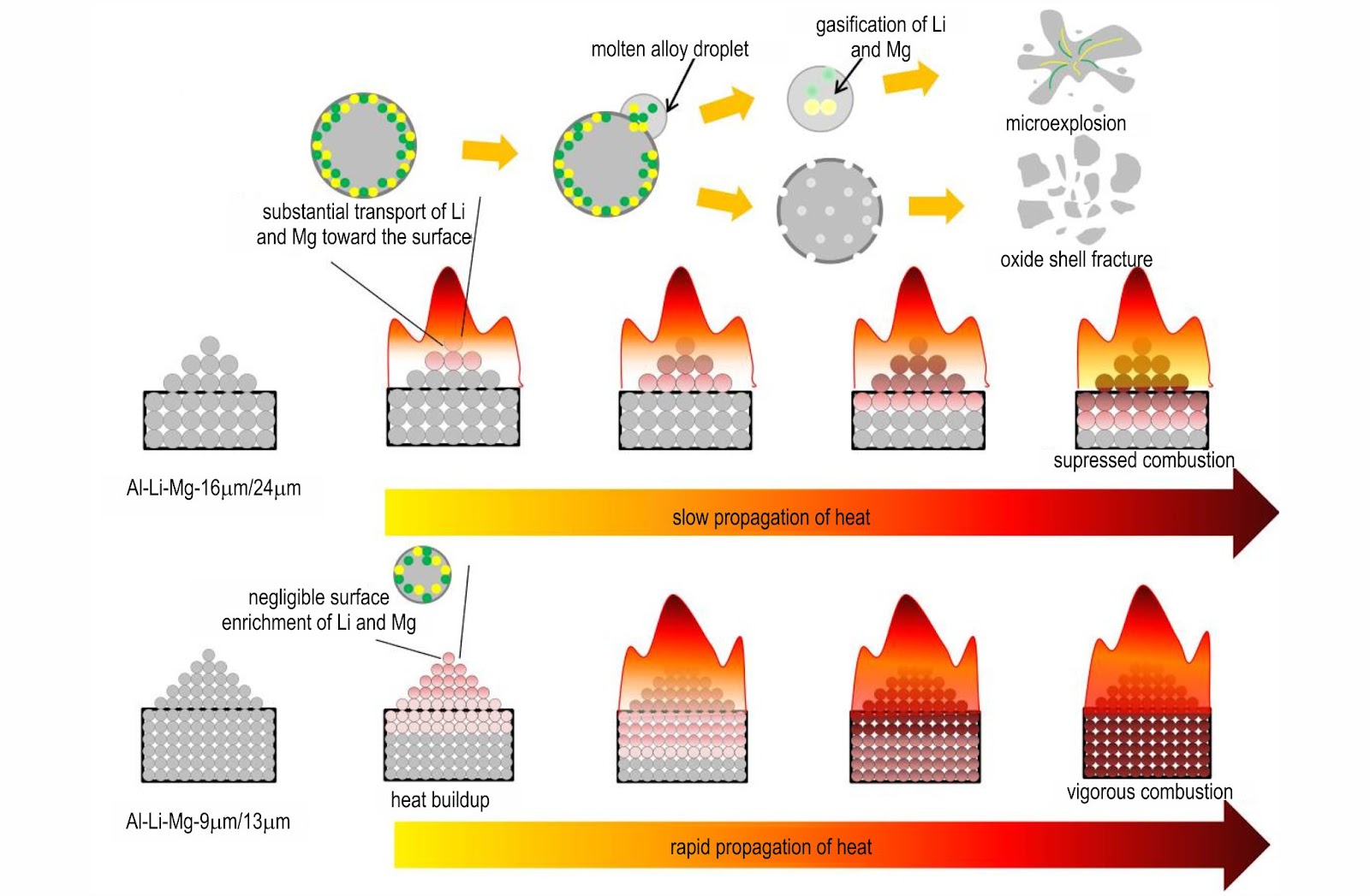
Effect of Particle Size on Ignition and Combustion Performance of Al-Li-Mg Alloys

Effect of Particle Size on Ignition and Combustion Performance of Al-Li-Mg Alloys

To elucidate the influence mechanism of particle size on the ignition and combustion behavior of Al-Li-Mg alloys, four alloy powders with median diameters of 9, 13, 16, and 24 μm were systematically investigated. Physicochemical properties were characterized by laser diffraction, scanning electron microscopy, X-ray diffraction, simultaneous thermal analysis, and oxygen bomb calorimetry. Ignition and combustion behaviors were assessed using a laser ignition test bench equipped with high-speed photography and fiber-optic spectrometry. Results show that with increasing particle size, ignition delay time first decreases sharply then stabilizes, dropping from 135 ms (9 μm) to 51 ms (13 μm), then to 15 ms (16 μm) and 18 ms (24 μm). Combustion intensity, indicated by maximum spectral intensity, decreases from 7300.4 (9 μm) to 1721.6 (24 μm). Combustion duration initially extends slightly then stabilizes, from 857 ms (9 μm) to 928 ms (13 μm) and approximately 920 ms for larger sizes. Notably, the 13 μm alloy achieves an optimal balance among ignition delay (51 ms), combustion duration (928 ms), and combustion intensity (6041.8). The study reveals a critical size effect: between 13 and 16 μm, ignition delay drops by 71% while combustion intensity decreases by 54%, indicating a transition from surface-diffusion-controlled to micro-explosion-dominated combustion. This mechanism arises from competition between heat conduction and elemental diffusion: larger particles restrict heat transfer, promoting Li and Mg surface enrichment and temperature gradients that induce micro-explosions, thereby shortening ignition delay but reducing combustion efficiency and intensity.

Examine Data & PDF
Research PaperYear: 2026
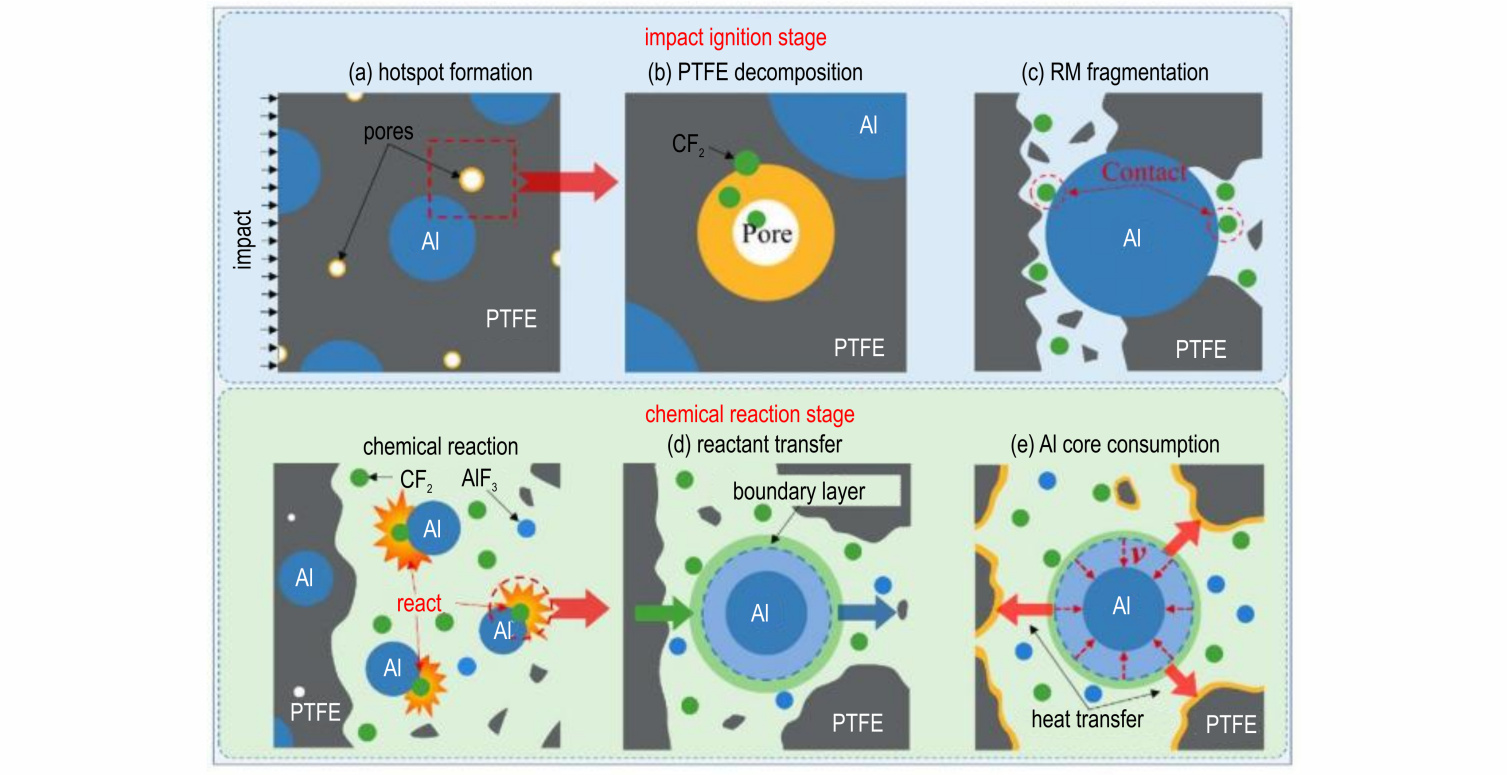
Research Progress on Dynamic Response and Energy Release Mechanisms of Reactive Damage Elements

Research Progress on Dynamic Response and Energy Release Mechanisms of Reactive Damage Elements

Reactive damage elements (RDEs) integrate kinetic penetration with chemical energy release, offering a dual-mode damage mechanism. This review systematically examines the state-of-the-art in RDE reaction mechanisms, penetration-reaction coupled damage models, numerical simulation methods, and dynamic loading experiments. Two-stage reaction mechanisms—shock-induced and shock-assisted—are elaborated, along with thermo-mechanical-chemical coupling theory and reaction threshold regulation. Penetration depth and hole-enlargement models, aftereffect overpressure and ignition models, fragment cloud distribution and damage radius models are summarized. Advances in reactive material equations of state, SPH-ALE multi-physics coupling algorithms, and cross-scale modeling methods are consolidated, alongside multi-physics synchronous testing and target damage assessment systems. Key findings include: Al-Ni-W systems achieve densities up to 7.8 g·cm⁻³ and tensile strengths exceeding 300 MPa, maintaining structural integrity at 2000 m·s⁻¹. PTFE/Al formulations exhibit shock-induced reactions in nanoseconds, while shock-assisted reactions occur over microseconds to milliseconds, with oxide additives like MoO₃ lowering reaction thresholds and enhancing energy release. Future directions emphasize precise reaction degree control via cross-scale models, universal damage assessment under extreme environments, and field testing using characteristic spectra and electromagnetic pulses. This review provides a comprehensive framework for advancing RDE technology in munitions and protective applications.

Examine Data & PDF
Research PaperYear: 2026
Deep Learning-Based Spectral Identification of Explosives: A Sequential Infrared and Raman Approach

Deep Learning-Based Spectral Identification of Explosives: A Sequential Infrared and Raman Approach

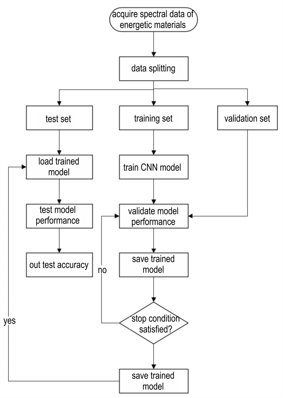
The complex composition of mixed explosives poses significant challenges to conventional detection methods, which often suffer from low intelligence and poor discrimination. This study addresses these limitations by employing a sequential detection framework combining infrared (IR) spectroscopy for preliminary screening and Raman spectroscopy for confirmatory analysis, integrated with convolutional neural networks (CNNs) for intelligent spectral recognition. Two energetic material mixtures, m-dinitrobenzene/potassium nitrate and p-nitroaniline/ammonium nitrate, were prepared in powder and tablet forms. IR spectroscopy effectively identified organic components through characteristic absorption peaks but failed to detect inorganic oxidizers such as potassium nitrate and ammonium nitrate. Raman spectroscopy successfully characterized nitroaromatic functional groups and detected inorganic ions, enabling complete component identification. The CNN-based models achieved average classification accuracies of 96.54% for IR spectra and 96.29% for Raman spectra, with per-sample inference times of 0.044 s and 0.042 s, respectively. These results demonstrate that the proposed sequential IR-Raman approach, coupled with deep learning, provides a rapid and reliable solution for field detection of mixed explosives, overcoming the limitations of single-spectroscopy methods.

Examine Data & PDF
Research PaperYear: 2026
Physical Trend for Critical Temperature in Bi2Sr2CaCu2O8 High-temperature Superconductors

Physical Trend for Critical Temperature in Bi2Sr2CaCu2O8 High-temperature Superconductors

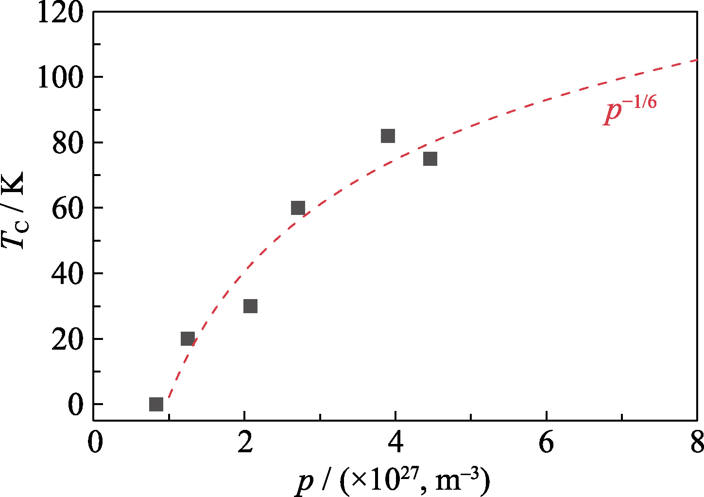
Superconductivity remains a central challenge in condensed matter physics and materials science, with high-temperature superconductors lacking a unified theoretical framework. This work investigates the relationship between critical temperature (TC) and hole concentration in Y-doped Bi2Sr2CaCu2O8 (Bi-2212), a cuprate superconductor. By systematically varying the hole concentration through Y substitution, we establish a power-law scaling: TC ∝ p^0.5, where p is the hole concentration per CuO2 plane. The exponent of 0.5 indicates a quadratic dependence, suggesting that increased hole concentration enhances superconducting pairing strength. Our data reveal that TC increases monotonically with hole concentration up to the optimal doping level, reaching a maximum of 95 K at p ≈ 0.16, beyond which over-doping suppresses superconductivity. This trend holds across the under-doped and optimally-doped regimes, providing a predictive tool for optimizing TC in Bi-2212 and related cuprates. The findings underscore that hole concentration is a critical control parameter, and achieving high TC requires precise doping control. This work offers practical guidance for the design of new high-temperature superconductors with enhanced performance, potentially enabling operation at liquid-nitrogen temperatures and above, which is crucial for technological applications such as magnetic resonance imaging, particle accelerators, and power transmission.

Examine Data & PDF
Research PaperYear: 2026
Influence of Preparation Processes on the Structure and Properties of the Ductile Thermoelectric Material Ag2S0.4Te0.6

Influence of Preparation Processes on the Structure and Properties of the Ductile Thermoelectric Material Ag2S0.4Te0.6

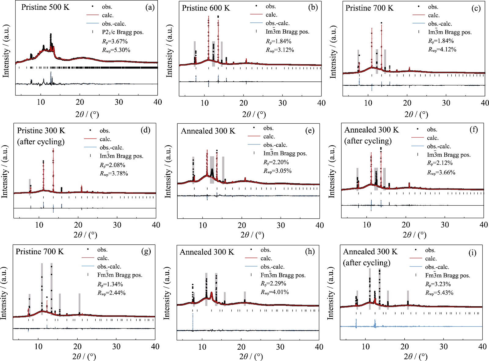
Ag2S0.4Te0.6 is an inorganic semiconductor with favorable ductility and thermoelectric performance, showing potential for applications in wearable electronics. Recent studies have indicated that optimization of preparation processes, such as annealing, can significantly enhance the ductility of the material, which is closely related to its phase composition and crystal structure. In this work, high-resolution synchrotron radiation powder X-ray diffraction data of the Ag2S0.4Te0.6 powder sample before and after annealing were collected over a temperature range of 110–700 K. By combining Rietveld structural refinement, high-resolution transmission electron microscopy, and atomic pair distribution function analysis, the influence of the annealing process on the phase composition and structural evolution behavior of the powder samples was investigated in detail. The results show that the pristine Ag2S0.4Te0.6 powder is predominantly amorphous, containing only a small amount of poorly crystalline monoclinic phase. During heating, the material gradually crystallizes, first forming a monoclinic phase, which subsequently transforms into mixed body-centered cubic (bcc) and face-centered cubic (fcc) phases. After cooling back to room temperature, the sample remains in a mixed state of bcc-dominated cubic crystallinity and amorphous phase. In contrast, the annealed powder sample already exhibits a mixed cubic crystalline/amorphous state at room temperature, and no obvious phase transition behavior is observed during heating. Moreover, the thermoelectric properties of Ag2S0.4Te0.6 bulk sample remain largely unaffected by the annealing process. This study provides structural insights for further understanding the annealing-induced improvement in ductility.

Examine Data & PDF
Research PaperYear: 2026
Research Progress on Controllable Synthesis of Blue-emitting ZnSeTe Quantum Dots and Quantum-dot Light-emitting Diode Devices

Research Progress on Controllable Synthesis of Blue-emitting ZnSeTe Quantum Dots and Quantum-dot Light-emitting Diode Devices

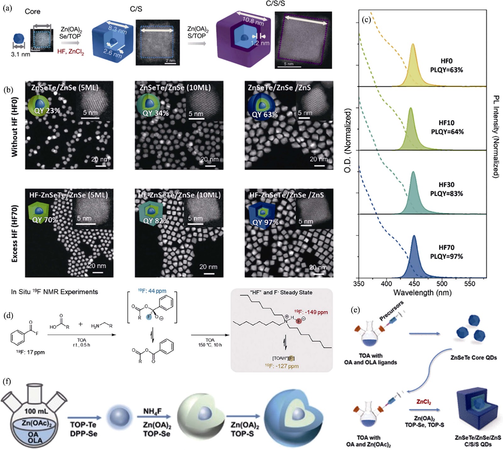
Colloidal quantum dots (QDs) are promising emissive materials for optoelectronic devices owing to their tunable emission wavelength, high color purity, and solution processability. Quantum-dot light-emitting diodes (QLEDs), an important complementary technology to organic light-emitting diodes, have demonstrated considerable potential in display applications. However, the inherent toxicity of conventional Cd- and Pb-based QDs has driven the development of heavy-metal-free QDs systems. Currently, heavy-metal-free blue QLEDs still lag significantly behind their red and green counterparts in device efficiency and operational stability, representing a critical bottleneck to their practical application. To address this issue, ZnSeTe QDs have attracted significant research interest due to their tunable bandgap and excellent blue emission properties. In this work, a comprehensive review of ZnSeTe QDs is provided. Firstly, their nucleation and growth mechanisms, as well as typical synthesis methods are introduced, and the key factors affecting their optical properties are discussed. On this basis, various performance optimization strategies, including band engineering, surface etching, shell passivation, and ligand regulation, are systematically summarized. Furthermore, electroluminescence mechanisms of QLEDs and recent progress on the application of ZnSeTe QDs in blue-emitting devices are reviewed. Finally, the current challenges, such as low emission efficiency, limited device lifetime, and charge injection imbalance, are discussed, and potential future development directions are proposed.

Examine Data & PDF
Research PaperYear: 2026
Crystallization-Sequence Engineering Enables Organic Solar Cell Modules with Efficiencies Exceeding 18%

Crystallization-Sequence Engineering Enables Organic Solar Cell Modules with Efficiencies Exceeding 18%

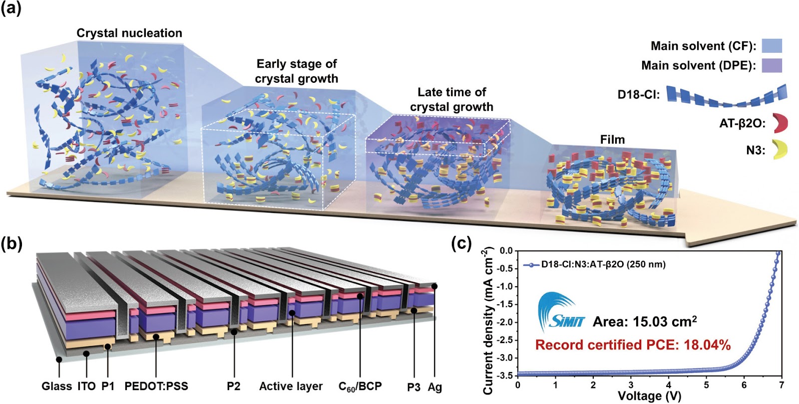
Organic solar cells (OSCs) have emerged as a promising photovoltaic technology due to their mechanical flexibility, low density, and compatibility with solution-based fabrication, enabling applications such as wearable electronics and building-integrated photovoltaics. Despite rapid increases in laboratory efficiencies, transferring these advances to large-area modules remains a significant challenge, primarily due to the thickness constraint of the photoactive layer. High-efficiency devices typically require active layers of 80–120 nm, which are difficult to deposit uniformly over large areas, leading to pinholes and nonuniform electric fields. Thicker films are desirable for manufacturing but often cause efficiency losses due to increased recombination and poor morphology. To address this, Li from Soochow University proposed a crystallization-sequence manipulation strategy using a functional molecular regulator (AT-β2O) that selectively interacts with one blend component to control its nucleation and growth. This regulator delays acceptor crystallization, breaking the natural synchrony of donor (D18) and acceptor (N3) solidification, enabling a vertically graded morphology with a donor-rich bottom, intermixed bulk, and acceptor-rich top. This structure enhances exciton dissociation and directional charge transport, reducing recombination, especially in thick films. Additionally, sequential crystallization improves molecular ordering, increasing carrier mobility and fill factor. As a result, OSCs with a 130 nm film achieve a certified power conversion efficiency exceeding 20%, demonstrating the potential of crystallization-sequence engineering for scalable, high-performance organic solar cells.

Examine Data & PDF
Research PaperYear: 2026
θ-TaN: Redefining the Thermal Conductivity Limit of Metallic Materials

θ-TaN: Redefining the Thermal Conductivity Limit of Metallic Materials

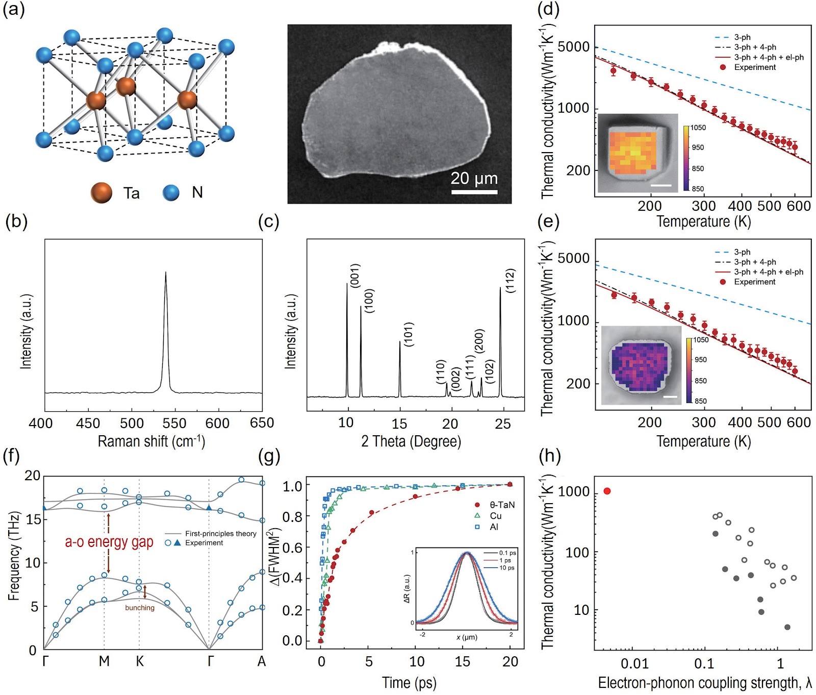
Thermal management has become a critical bottleneck for the performance and reliability of modern electronics. For over a century, the thermal conductivity (κ) of metallic materials was believed to have an inherent upper limit of approximately 400 W·m⁻¹·K⁻¹, constrained by strong electron-phonon coupling and lattice anharmonicity. However, a groundbreaking study by Li et al. (Science, 2026) experimentally realized single-crystalline θ-phase tantalum nitride (θ-TaN), a metastable transition metal nitride with a room-temperature thermal conductivity of ~1100 W·m⁻¹·K⁻¹ along the a-axis and ~928 W·m⁻¹·K⁻¹ along the c-axis, nearly three times that of copper. This work shatters the long-standing thermal conductivity limit for metals and validates theoretical predictions. The exceptional performance of θ-TaN arises from its unique hexagonal crystal structure (space group P6m2), featuring a large acoustic-optical phonon gap (~8 THz) and acoustic phonon bunching, which suppress phonon-phonon scattering. Additionally, weak electron-phonon coupling and minimal isotope scattering contribute to phonon-dominated heat transport. The authors synthesized high-quality single crystals via a flux-assisted metathesis reaction, overcoming challenges of conventional high-pressure routes. Using time-domain thermoreflectance and inelastic X-ray scattering, they confirmed the intrinsic ultrahigh thermal conductivity and mapped the phonon band structure. This discovery introduces a new class of high-thermal-conductivity metals, opening transformative opportunities for thermal management in electronics, aerospace, and energy systems.

Examine Data & PDF
Research PaperYear: 2026
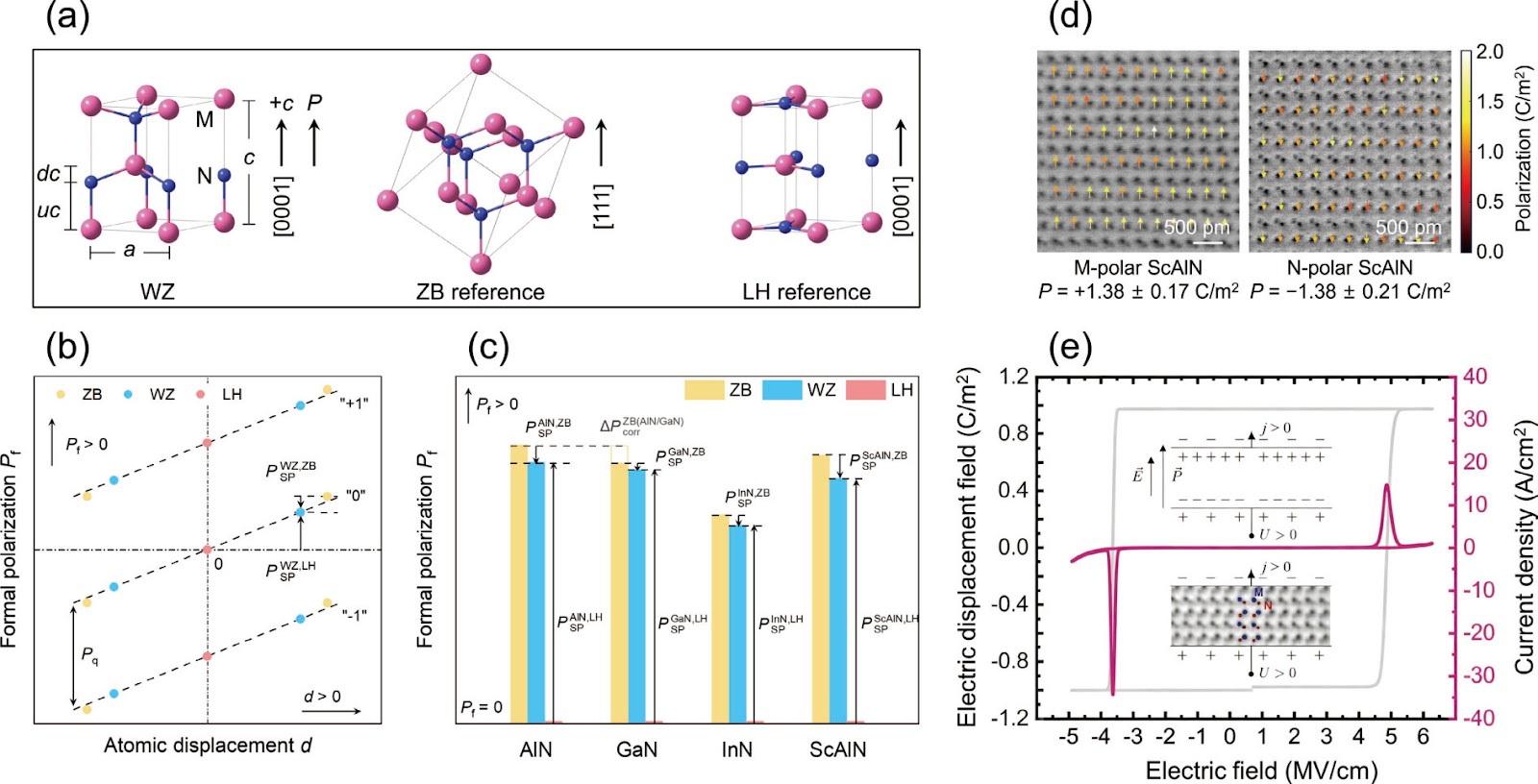
Zigzag Domain Walls Unravel the Polarization Switching Puzzle in Wurtzite Ferroelectrics

Zigzag Domain Walls Unravel the Polarization Switching Puzzle in Wurtzite Ferroelectrics

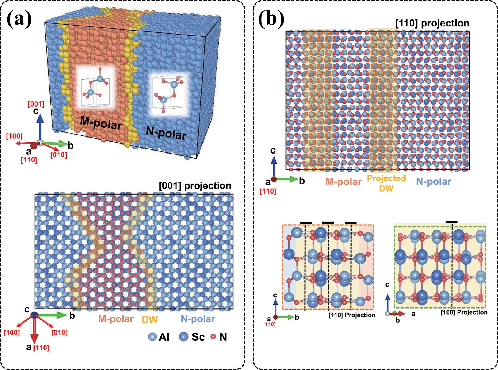
The discovery of robust ferroelectricity in scandium-doped aluminum nitride (Al1−xScxN) has sparked significant interest due to its compatibility with CMOS fabrication, making it a promising candidate for next-generation non-volatile memories and high-frequency devices. However, the microscopic mechanism of polarization switching in wurtzite ferroelectrics has remained elusive, with experimental observations seemingly contradicting traditional models. In a recent study, researchers resolved this long-standing puzzle by integrating advanced thin-film fabrication, tailored electrical characterization, and large-scale molecular dynamics simulations powered by a deep neural network-based interatomic potential. Their findings reveal that the broad 'transitional regions' observed in scanning transmission electron microscopy (STEM) are not a new nonpolar phase but a projection artifact arising from intrinsically three-dimensional zigzag domain walls. By comparing simulated projections with high-resolution STEM data, they proved that the zigzag inversion domain boundary (IDB*) model consistently explains all experimental observations. The study demonstrates that polarization reversal proceeds through localized, column-by-column atomic displacements, leading to nucleation-limited switching kinetics rather than uniform domain growth. Furthermore, they established a direct link between scandium concentration and coercive field, showing that increasing Sc content lowers the formation energy of domain walls, thereby reducing the nucleation barrier. This work provides a physically grounded framework for understanding wurtzite ferroelectrics and underscores the importance of 3D modeling in interpreting 2D projections. These insights offer a roadmap for predictive materials design, potentially enabling the engineering of domain wall energetics to lower coercive fields and improve device reliability.

Examine Data & PDF
Research PaperYear: 2026
Investigation of Multiphase Fluid Seepage Behaviour in Abandoned Mines: Insights from Single Fracture to Network Scale

Investigation of Multiphase Fluid Seepage Behaviour in Abandoned Mines: Insights from Single Fracture to Network Scale

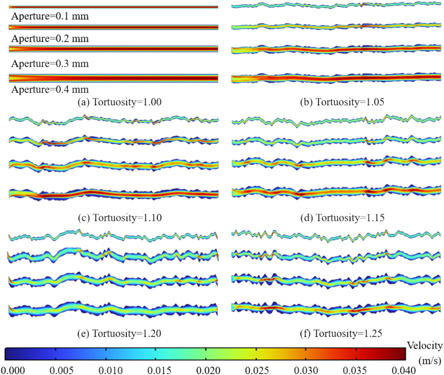
Quantifying two-phase fluid flow in fractured rocks is essential for resource reutilization in abandoned mines, subsurface energy recovery and underground waste isolation. This study develops a mathematical framework for predicting the permeability of rough fracture networks by integrating fractal geometry with single-phase and two-phase seepage theory. A permeability model for rough fracture networks is first established, and its sensitivity to key geometric parameters is analyzed. A second model is then formulated to relate water-phase saturation to measurable variables, enabling the estimation of two-phase permeability from Reynolds number and aperture. Model predictions show deviations of less than 10% from numerical simulations for both single-phase and two-phase flow, demonstrating the accuracy and robustness of the proposed approach. The results highlight the dominant roles of fracture number, tortuosity and aperture in controlling permeability, as well as the influence of flow regimes on relative permeability. The proposed framework provides a practical and physically based method for analyzing multiphase seepage in fractured rock and offers a foundation for further applications to field-scale fractured systems.

Examine Data & PDF
Research PaperYear: 2026
Crystallization Suppression of Mixed-Halide Intermediates for Perovskite/Cu(In,Ga)Se2 Tandem Solar Cells with Improved Efficiency

Crystallization Suppression of Mixed-Halide Intermediates for Perovskite/Cu(In,Ga)Se2 Tandem Solar Cells with Improved Efficiency

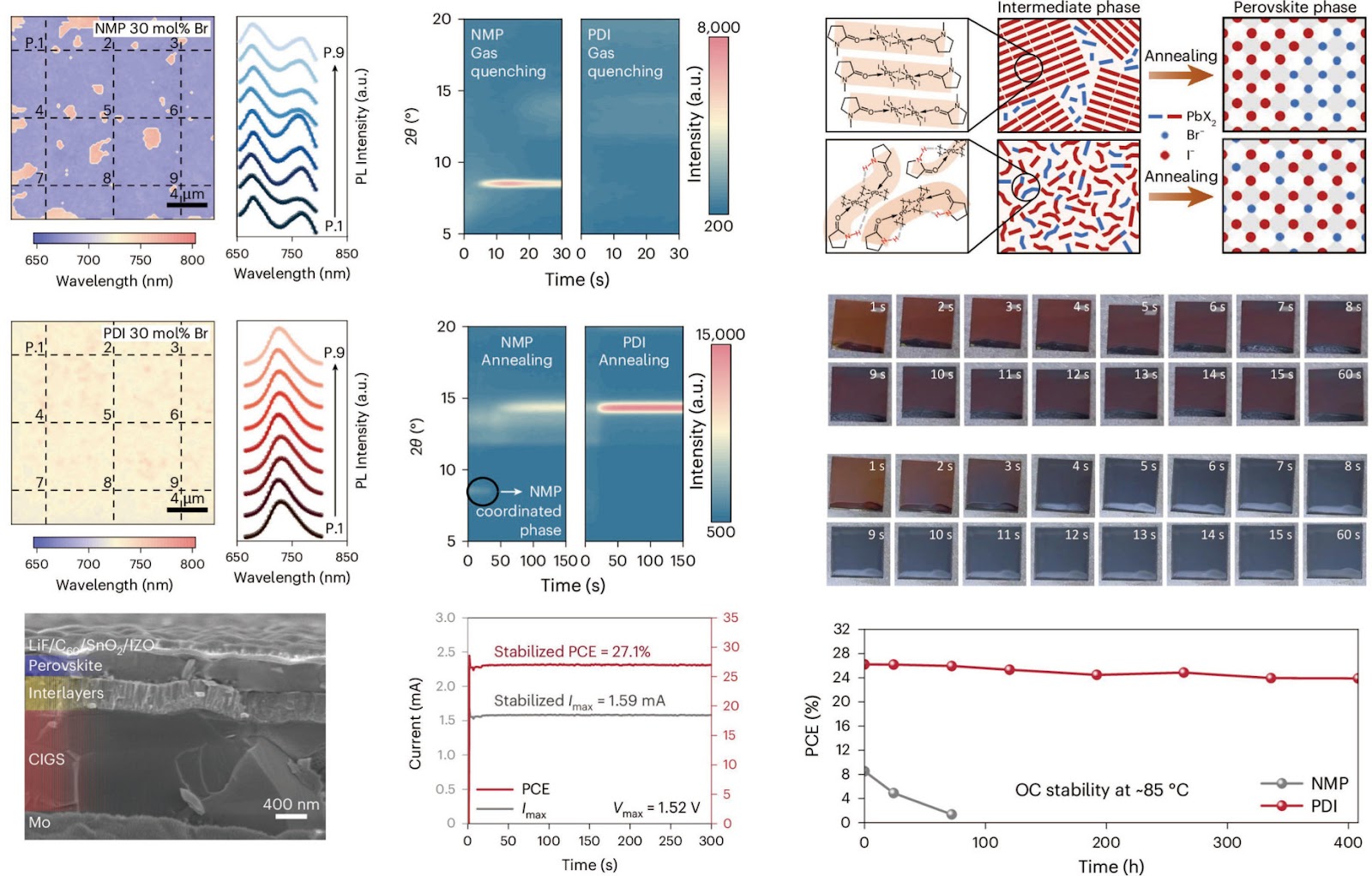
Flexible and lightweight photovoltaics are pivotal for renewable energy applications, and all-thin-film tandem solar cells combining metal-halide perovskites with copper indium gallium selenide (CIGS) offer a synergistic approach to exceed the Shockley-Queisser limit. However, fabricating high-quality wide-bandgap (WBG) perovskite films, especially via scalable blade-coating in ambient air, remains challenging due to uncontrollable crystallization kinetics, phase segregation, and moisture-induced defects. This work addresses these issues by introducing a crystallization suppression strategy that replaces the traditional solvent N-methyl-2-pyrrolidone (NMP) with 2-pyrrolidinone (PDI). In situ grazing-incidence X-ray diffraction (GIXRD) reveals that NMP-based films undergo a crystalline-to-crystalline transition via solvent-coordinated intermediates, leading to residual impurities and incomplete phase transformation. In contrast, PDI, through additional hydrogen bonding, suppresses pre-crystallization and maintains a homogeneous non-crystalline precursor state, enabling a rapid non-crystalline-to-crystalline transition with lower energy barriers. This results in uniform, pinhole-free films with enhanced carrier mobility, longer carrier lifetimes, and reduced trap densities. Single-junction perovskite solar cells fabricated with PDI achieve significantly improved efficiency, demonstrating the effectiveness of this approach for high-performance perovskite/CIGS tandem solar cells.

Examine Data & PDF
Research PaperYear: 2026
Exciplex-Enabled Fully Stretchable OLEDs Achieve a Record External Quantum Efficiency of 17%

Exciplex-Enabled Fully Stretchable OLEDs Achieve a Record External Quantum Efficiency of 17%

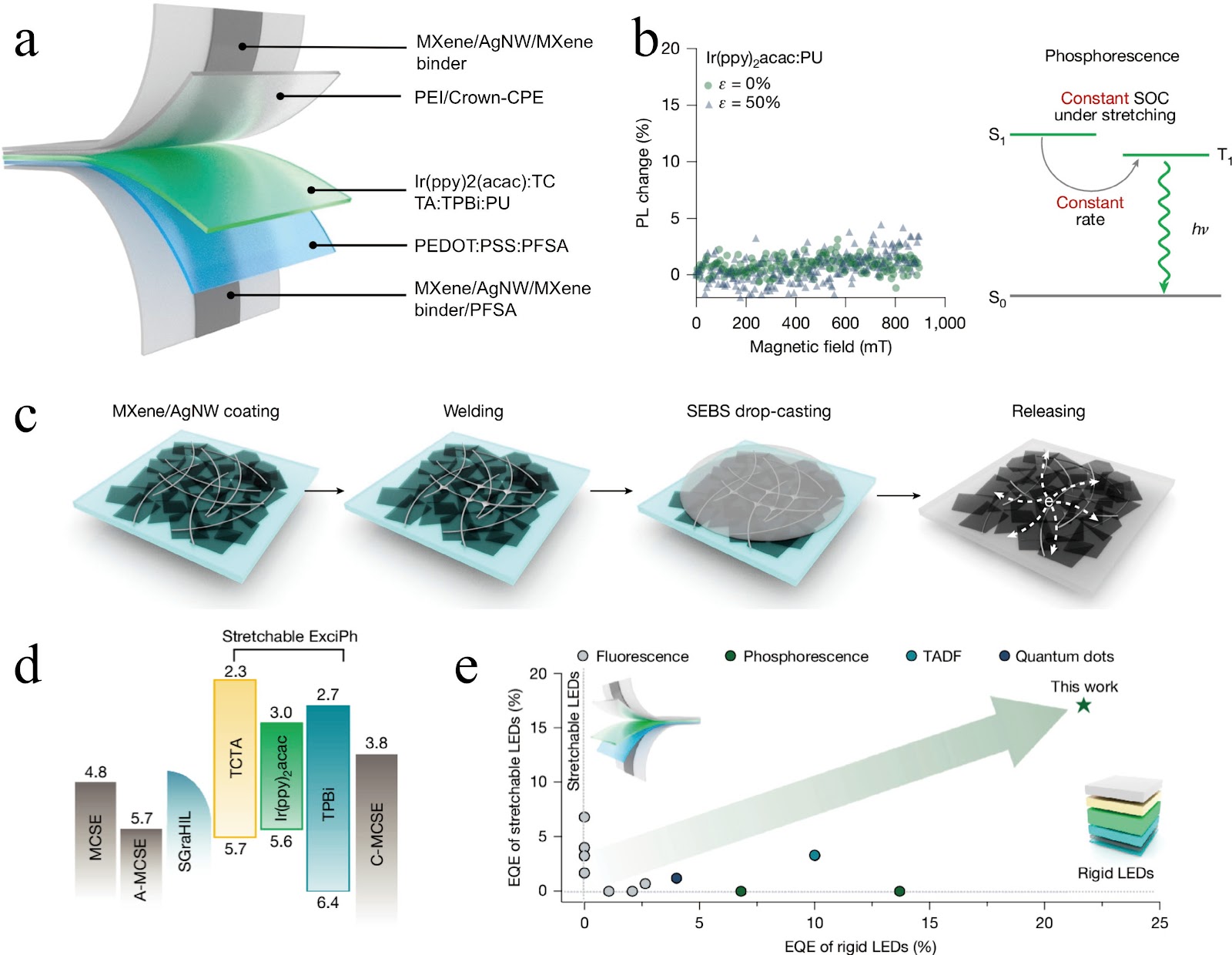
Organic light-emitting diodes (OLEDs) are promising candidates for on-skin applications due to their intrinsic stretchability. However, the external quantum efficiency (EQE) of stretchable OLEDs has long been limited to approximately 10%, stemming from the incorporation of insulating elastomer matrices that hinder exciton energy transfer and charge transport, and from conventional stretchable electrodes with insufficient electrical properties and poor interfacial contact. In a recent breakthrough published in Nature (2026), Gogotsi and Lee reported an exciplex-enabled strategy that overcomes these limitations. By integrating a stretchable exciplex-assisted phosphorescent emitting layer, triplet harvesting is significantly enhanced through an elastomer-tolerant triplet-recycling mechanism. Furthermore, they employ work-function-tunable MXene-contact stretchable electrodes (MCSEs) that provide two-dimensional electrical contact for efficient charge injection. Combining these advances, they achieve an unprecedented EQE of 17% in fully stretchable OLEDs while maintaining excellent mechanical stability. The spin-flip process, which converts non-radiative triplets into radiative singlets, is critical yet challenging in stretchable OLEDs because the necessary spin-orbit coupling (SOC) is sensitive to variations in intermolecular distance under strain. The authors utilize the phosphorescent emitter bis(2-phenylpyridine) (Ir(ppy)2acac), whose heavy-metal iridium center provides strong SOC, enabling nearly complete intersystem crossing and triplet utilization. The study demonstrates that the intrinsic SOC of Ir(ppy)2acac remains stable under 50% tensile strain, preserving both spin-mixing rates and photoluminescence stability. To prevent aggregation-induced quenching and enable efficient energy transfer within a soft matrix, the authors develop a stretchable exciplex-assisted phosphorescent (ExciPh) layer using TCTA and TPBi to form an exciplex cohost, while a thermoplastic polyurethane (PU) elastomer provides mechanical stretchability. This system enables triplet excitons to undergo reverse intersystem crossing (RISC) within a charge-transfer state, followed by long-range Förster resonance energy transfer (FRET) to the phosphorescent dopant. The fabricated OLED demonstrates an EQE of 21.7%, validating the effectiveness of this approach. Beyond the emissive layer, the researchers develop MXene-conductive stretchable electrodes (MCSEs) by integrating a two-dimensional MXene interlayer with silver nanowire (AgNW) networks, achieving a sheet resistance of ~30 Ω/sq with over 85% transmittance at 550 nm and a widely tunable work function (3.79–5.71 eV). They also introduce a stretchable gradient hole injection layer (SGraHIL) that suppresses exciton quenching at the interface while maintaining excellent stretchability. By integrating the SGraHIL, the ExciPh emitting layer, and MCSE electrodes, the authors fabricate fully stretchable OLEDs that achieve an unprecedented EQE of 17%, retaining 83% of initial efficiency after 100 cycles of 20% cyclic strain. This work represents a significant advance in intrinsically stretchable optoelectronics, offering a scalable route toward highly conductive, work-function-tunable contacts and influencing broader fields such as stretchable sensors and soft photonic systems.

Examine Data & PDF
Research PaperYear: 2026
One-dimensional domain walls: A new dimension for ferroelectric nanoelectronics

One-dimensional domain walls: A new dimension for ferroelectric nanoelectronics

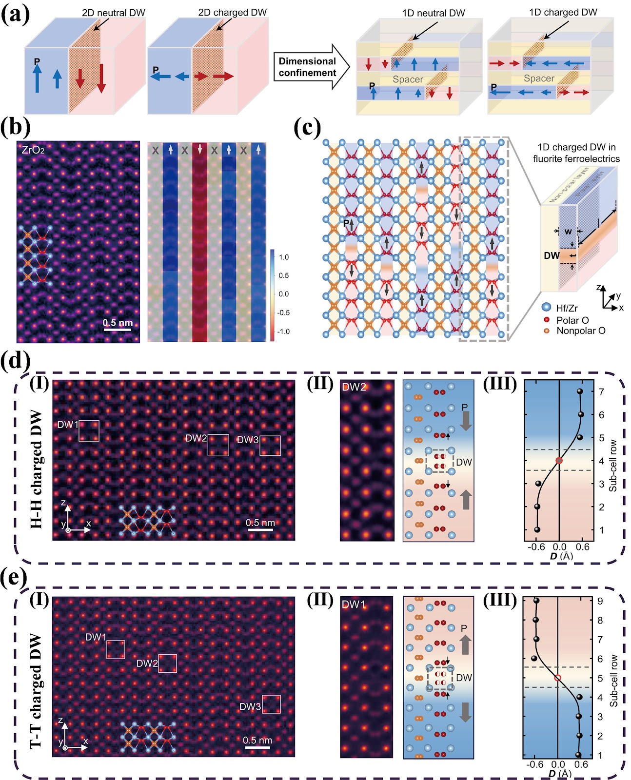
Topological structures in ferroelectric materials, such as vortices, skyrmions, and merons, have attracted significant attention due to their emergent physical properties distinct from the bulk parent phase. Among these, ferroelectric domain walls (DWs) have long been considered potential active elements for next-generation electronic devices, leading to the paradigm of "domain wall nanoelectronics." However, conventional perovskite ferroelectrics exhibit two-dimensional (2D) domain walls, and charged domain walls (CDWs) suffer from structural broadening due to electronic screening, limiting miniaturization. Recently, a research team led by Chen Ge, Kui-juan Jin, and Qinghua Zhang from the Institute of Physics, Chinese Academy of Sciences, reported the groundbreaking observation of one-dimensional (1D) CDWs in fluorite-structured ferroelectric ZrO2, achieving atomic-scale confinement. Using multislice electron ptychography, they visualized head-to-head and tail-to-tail CDWs with atomic-scale width and thickness (~2.55 Å and ~2.7 Å), equivalent to a single subcell unit. The stability of these atomically thin walls is attributed to a distinct ionic screening mechanism: self-balanced oxygen nonstoichiometry, where H–H walls accumulate excess oxygen ions and T–T walls harbor oxygen vacancies. Furthermore, in situ electric-field experiments demonstrated dynamic manipulation of these 1D structures, revealing a coupling between polarization switching and oxygen ion transport. This discovery breaks the inherent physical limitations of perovskite ferroelectrics and opens new avenues for high-density ferroelectric nanoelectronics.

Examine Data & PDF
Research PaperYear: 2026
Large-scale integrated photonic accelerators for ultralow-latency and universal AI computing

Large-scale integrated photonic accelerators for ultralow-latency and universal AI computing

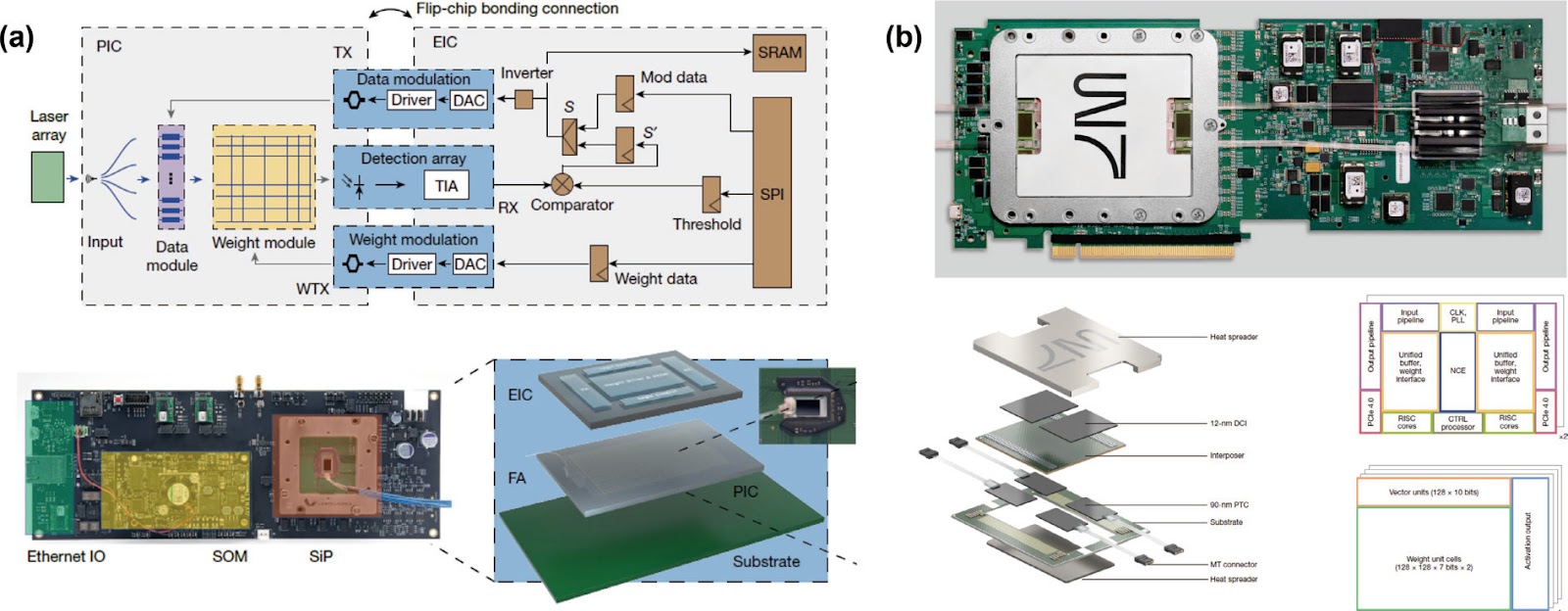
Integrated silicon photonics has emerged as a transformative technology for post-Moore's law computing, offering intrinsic advantages of high bandwidth, ultralow latency, and low energy consumption that far exceed traditional electronic computing architectures. As artificial intelligence (AI) models continue to grow in complexity and scale, the demand for high-speed, energy-efficient computing has spurred intensive research into photonic computing as a promising alternative to electronic accelerators. Matrix multiply-accumulate (MAC) operations, the core of deep learning and combinatorial optimization algorithms, are particularly amenable to photonic implementation, as light enables parallel multiplication and accumulation with minimal data movement. However, the practical application of photonic computing has long been hindered by critical challenges including large-scale integration of photonic components, electro-optical co-packaging, guaranteed computation accuracy of analog photonic systems, and compatibility with mainstream AI models and algorithms. Recently, two groundbreaking studies published back-to-back in Nature have achieved pivotal breakthroughs in addressing these bottlenecks, demonstrating large-scale integrated photonic accelerators with ultralow latency for combinatorial optimization and universal AI computing capabilities for state-of-the-art neural networks. The two works represent the most advanced level of photonic computing hardware implementation to date, validating the feasibility of photonic accelerators as a competitive alternative to electronic AI chips and marking a critical step toward the commercialization of integrated photonic computing technology.

Examine Data & PDF
Research PaperYear: 2026
Re-benchmarking Polarization in Wurtzite Nitride Semiconductors

Re-benchmarking Polarization in Wurtzite Nitride Semiconductors

Polarization is a defining lever of wurtzite (WZ) III-nitrides, enabling two-dimensional electron and hole gases, polarization doping, and electrostatic control in GaN-based power, RF, and optoelectronic devices. Recent advances, especially ferroelectric nitrides, have pushed polarization to unprecedented magnitudes, elevating it from a static constant to an engineering knob. However, the field has long suffered from ambiguity in polarization magnitude, orientation, and mapping to crystal polarity due to inconsistent sign conventions and reference choices. This mini-review highlights recent progress that rethinks and unifies polarization in wurtzite III-nitrides. It discusses how experimental re-benchmarking of giant polarization is reshaping understanding and enabling predictive polarization engineering. Key issues include the dependence of polarization sign on coordinate choice and magnitude on reference structure, as exemplified by Bernardini et al.'s 1997 predictions (values below 0.1 C/m², downward orientation for metal-polar) and Dreyer et al.'s 2016 refinements. The review emphasizes that consistent benchmarking under a unified convention makes interface bound charge density a quantitative design knob rather than an adjustable fitting parameter, benefiting classical HEMTs, N-polar stacks, polarization-doped structures, and ferroelectric nitride integration. A pragmatic roadmap is proposed: reports should state polarity, sign convention, and reference explicitly to ensure portability and falsifiability.

Examine Data & PDF
Research PaperYear: 2026
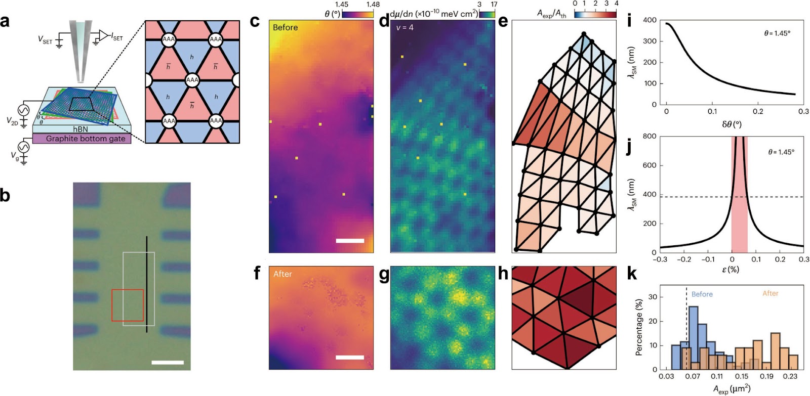
Supermoiré Domains in Helical Trilayer Graphene

Supermoiré Domains in Helical Trilayer Graphene

Helical trilayer graphene (HTG), composed of three graphene layers with equal twist angles in the same rotational sense, has emerged as a rich platform for studying moiré physics. Theoretical predictions suggest that lattice relaxation in HTG leads to the formation of triangular domains with uniform moiré wavelength, arranged on a larger supermoiré length scale, with adjacent domains carrying opposite Chern numbers and hosting topological boundary modes. In a recent study, Hoke and colleagues directly imaged this supermoiré landscape using a scanning single-electron transistor (SET) probe sensitive to local electronic compressibility. Their measurements revealed a periodic modulation with a length scale of several hundred nanometers, far exceeding the moiré wavelength, consistent with theoretical predictions. The spatial maps showed a triangular lattice of domain centers and a honeycomb network of AAA-stacking regions, separated by domain walls with reduced compressibility. Notably, the observed domain areas deviated from ideal expectations, indicating the presence of heterostrain. Modeling showed that biaxial strain applied to the middle layer can substantially enhance the supermoiré wavelength, with a divergence at a critical strain. After thermal cycling, the device exhibited larger and more isotropic supermoiré domains while the local twist angle remained unchanged, demonstrating that strain can be used to engineer the supermoiré network without perturbing local moiré physics. These findings underscore that lattice relaxation and strain are powerful tuning parameters in twistronics, with implications for engineering topological and correlated phases in twisted multilayers.

Examine Data & PDF
Research PaperYear: 2026
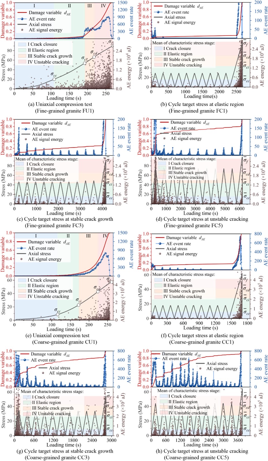
Estimation of characteristic stresses in granite through acoustic emission monitoring of microcrack fracture mode evolution

Estimation of characteristic stresses in granite through acoustic emission monitoring of microcrack fracture mode evolution

Characteristic stresses are critical indicators for microcrack initiation and propagation in rock, a process intrinsically linked to fracture mode. To investigate fracture mode evolution and its feasibility for estimating characteristic stresses, this study conducted uniaxial compression and cyclic loading-unloading tests on fine- and coarse-grained granite with acoustic emission (AE) monitoring. Cyclic target stresses were set within intervals determined by characteristic stresses. Analysis using the AE parameters AF-RA revealed that fracture mode evolution correlates with damage level, and shear microcrack propagation primarily governs macroscopic failure. A characteristic stress estimation method was developed by mapping key points on the shear crack proportion curve: crack closure stress (transition between fluctuating and stable segments), crack initiation stress (inflection point of curve rise), and crack damage stress (slope change point in ascending segment). Comparative analysis with the crack volumetric strain method validated the proposed method. The influences of fracture mode dividing line and statistical interval were discussed, with practical recommendations provided. Compared to conventional AE parameters, the fracture mode proportion exhibits lower sensitivity to AE parameter variations, enabling more reliable identification of characteristic stress points. Furthermore, it directly reflects microcrack evolution behavior, enhancing interpretability and providing a novel perspective for AE-based characteristic stress determination.

Examine Data & PDF
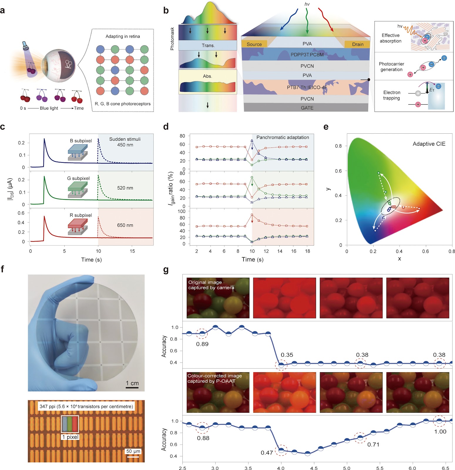
Research PaperYear: 2026
Three-Panchromatic Organic Self-Adaptive Transistors for In-Pixel Color Correction

Three-Panchromatic Organic Self-Adaptive Transistors for In-Pixel Color Correction

Machine vision systems face a fundamental challenge of illumination-dependent color shift, which conventional post-capture white-balance correction methods address at the cost of computational overhead and latency. Inspired by the human retina's chromatic adaptation, we propose a three-panchromatic organic self-adaptive transistor (OAAT) that embeds color correction directly at the pixel level. The device integrates a dual-layer complementary bulk heterojunction (BHJ) into an organic transistor architecture: a PTB7-Th:IEICO-4F blend serves as the adaptive photoresponse layer with broad-spectrum absorption and wavelength-insensitive trap activation energy that decreases with light intensity, while a PDPP3T:PCBM layer provides spectrally compensatory sensing. This design enables rapid, stable, and intensity-dependent photoadaptation, with an active adaptation index exceeding 150 for red, green, and blue stimuli. Under spectrally biased illumination, the device's responses follow von Kries coefficients and converge to a white-like chromatic state within seconds, demonstrating true chromatic adaptation. Wafer-scale fabrication achieved a 96.1% yield across 256 transistors, with pixel density of 347 ppi and over one million pixels integrated on a four-inch sapphire substrate. In a hybrid artificial visual system combining the OAAT array with a lightweight CNN, in-sensor correction restored classification accuracy for 'frog' in CIFAR-10 from 59.1% to 96.3% under blue-light interference, and outperformed conventional RGB cameras in real-world non-uniform lighting. This work presents a scalable, hardware-based solution for in-pixel color correction, promising for energy-efficient and real-time machine vision.

Examine Data & PDF
Research PaperYear: 2026
A Transferable Route to Two-Dimensional Gate-All-Around Electronics

A Transferable Route to Two-Dimensional Gate-All-Around Electronics

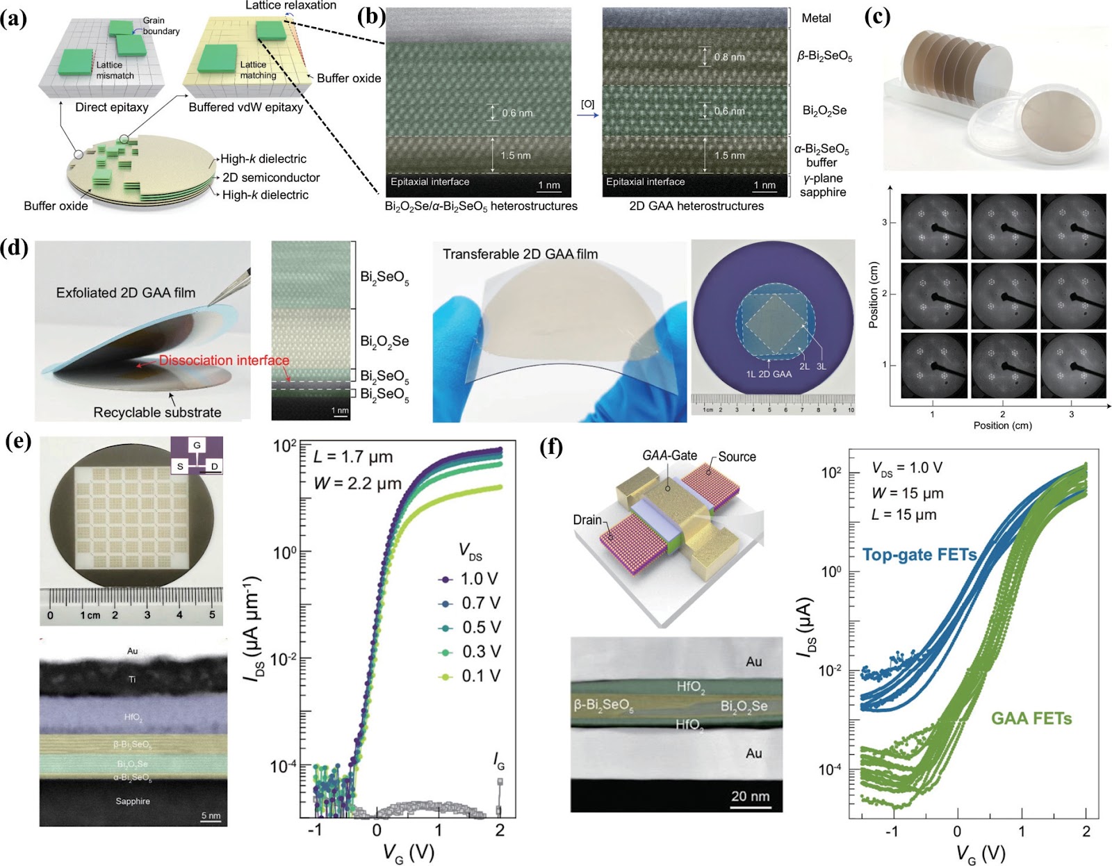
The relentless drive for miniaturization in microelectronics, guided by Moore's Law, is approaching a critical inflection point. Silicon-based transistors are confronting fundamental physical limits at the atomic scale, where issues of power leakage and degraded electrostatic control become increasingly severe. To sustain performance scaling, the semiconductor industry is transitioning to gate-all-around (GAA) nanosheet architectures for sub-2-nanometer technology nodes. However, integrating atomically thin two-dimensional (2D) semiconductors as channel materials within GAA structures offers a revolutionary path, promising superior electrostatic control and lower power consumption. The grand challenge has been the absence of a scalable, industry-compatible method to synthesize high-quality, uniform 2D semiconductor channels seamlessly encapsulated by high-k gate dielectrics in a GAA configuration. A groundbreaking study by Peng et al. reports the wafer-scale, uniform synthesis of single-crystalline 2D high-k dielectric/semiconductor/high-k dielectric GAA heterostructures via an innovative buffered van der Waals epitaxy technique. The core innovation lies in pre-depositing a high-k van der Waals buffer oxide (α-Bi2SeO5) on an r-plane sapphire substrate, which mitigates lattice mismatch and enables epitaxial growth of uniform Bi2O2Se films. Controlled oxidation transforms the top layer into β-Bi2SeO5, forming a sandwich-like GAA heterostructure with atomically sharp interfaces. The intrinsic transferability of these stacks allows clean exfoliation and transfer onto arbitrary substrates, leaving the sapphire wafer reusable. Field-effect transistors fabricated from these heterostructures exhibit outstanding electrical characteristics: on/off ratios exceeding 10^6 and carrier mobility up to 227 cm²·V⁻¹·s⁻¹. True GAAFETs using both top and bottom gates show improved subthreshold swing and higher on/off ratios, demonstrating superior gate controllability. This work represents a foundational platform technology addressing critical integration challenges for 2D semiconductors, bridging laboratory exploration and foundry-level manufacturing, and enabling monolithic 3D integration for future electronics.

Examine Data & PDF
Research PaperYear: 2026
Ultrathin van der Waals Ferroelectric Oxides for Scalable Low-Power Memory

Ultrathin van der Waals Ferroelectric Oxides for Scalable Low-Power Memory

The continuous scaling of ferroelectric memories to below 5 nm has exacerbated challenges such as depolarization fields, interfacial charge trapping, and structural non-uniformity, which critically bottleneck the performance and consistency of ferroelectric field-effect transistors (FeFETs). Although van der Waals ferroelectrics offer a promising route to overcome interface-related issues and critical-thickness limits, the lack of wafer-scale, CMOS-compatible ultrathin ferroelectric materials with robust polarization and high dielectric constants has hindered practical deployment. In a recent study published in Science (2026), Peng and colleagues report a wafer-scale, ultrathin van der Waals ferroelectric oxide platform that addresses these challenges via a controlled oxidation strategy, transforming a two-dimensional semiconductor precursor into a layered ferroelectric oxide with atomically smooth and chemically coherent interfaces. This native-oxide approach enables robust and switchable polarization down to the monolayer limit, as demonstrated by domain writing and erasing. The platform supports monolithic integration of FeFET arrays over centimetre-scale areas, exhibiting consistent hysteresis windows and switching thresholds across hundreds of devices, with narrow distributions of on/off ratios and threshold voltages. Furthermore, the programmable coupling between ferroelectric polarization and semiconductor channels enables multi-level threshold voltage programmability and stable switching between logic states, positioning these devices as reconfigurable building blocks for low-power memory and computing-in-memory architectures. This work bridges the gap between atomic-scale ferroelectric physics and manufacturable device architectures, offering a scalable path for next-generation non-volatile memory.

Examine Data & PDF
Research PaperYear: 2026
Material Platforms for Solid-State Single-Photon Sources: Wide Bandgap Semiconductors

Material Platforms for Solid-State Single-Photon Sources: Wide Bandgap Semiconductors

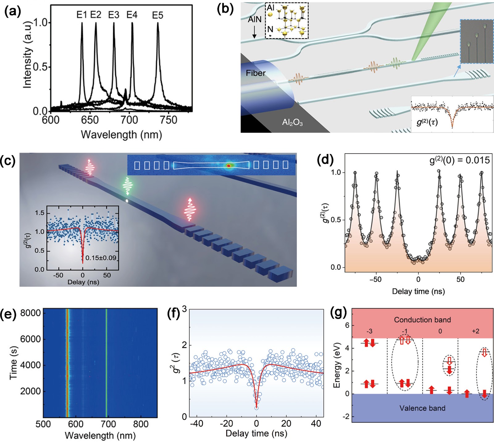
Single-photon sources are indispensable for scalable quantum information technologies, including quantum communication, key distribution, computing, and sensing. Optically active point defects in solid-state materials, known as color centers, are promising candidates for next-generation single-photon emitters (SPEs) due to their atom-like properties, enabling high efficiency, purity, and indistinguishability, while their solid-state nature facilitates integration into scalable quantum photonic devices. Among these, color centers in wide-bandgap semiconductors are particularly attractive for their stable operation at room temperature or higher and wide spectral tunability. Their compatibility with mature semiconductor technology allows direct integration into practical optoelectronic systems. Recent progress has realized defect-based SPEs in diamond, silicon carbide (SiC), silicon nitride (Si3N4), gallium nitride (GaN), aluminum nitride (AlN), hexagonal boron nitride (h-BN), zinc oxide (ZnO), and beta-phase gallium oxide (β-Ga2O3). This mini-review summarizes recent advances in SPEs based on wide-bandgap semiconductors, highlighting their potential for integrated quantum photonic circuits. Key platforms include diamond, hosting nitrogen-vacancy (NV) centers and group-IV impurity-based defects (SiV, GeV, SnV, PbV) with narrow emission lines and nanosecond lifetimes; Si3N4, where native defects in nitrogen-rich films exhibit linearly polarized emission at 567–670 nm with saturated room-temperature single-photon intensity of 5×10^5 cps; and h-BN, with an ultrawide bandgap of ~6 eV, enabling ultrabright, polarized single-photon emission at room temperature, with carbon-related defects (VBCN−) identified as visible quantum emitters. Challenges remain in structural identification and spectral uniformity, but controlled synthesis and strain engineering offer pathways to scalable quantum photonics.

Examine Data & PDF
Research PaperYear: 2026
Research Progress on the Structural Design and Common Preparation Technologies of Thermal Barrier Coatings

Research Progress on the Structural Design and Common Preparation Technologies of Thermal Barrier Coatings

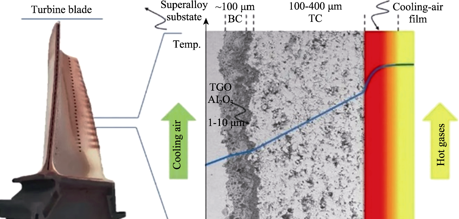
To address the severe challenges faced by high-temperature components in extreme environments, thermal barrier coating (TBC) technology has become a critical approach to enhance their operating temperature tolerance and extend service life. This paper systematically reviews the research progress on the structural design and common preparation technologies of thermal barrier coatings, focusing on the evolutionary logic and performance characteristics of double-layer and multi-layer structures. It specifically analyzes double-layer structures on nickel-based superalloys, steels, and aluminum alloys, as well as multi-layer structures, dual bond coat + ceramic layer structures, and bond coat + multi-layer ceramic structures obtained through different preparation techniques. The article also elaborates on the intrinsic correlation between the microstructure and coating performance of TBCs prepared by two mainstream techniques: atmospheric plasma spraying (APS) and electron beam physical vapor deposition (EB-PVD). Research indicates that double-layer structures have been widely applied due to their good comprehensive performance; while multi-layer/composite structures constructed with A2B2O7-type ceramic materials show more promising application prospects in terms of temperature resistance, thermal cycling life, and corrosion resistance. In response to the current bottlenecks in TBC technology development, this paper looks forward to key future directions for high-performance TBCs from multiple dimensions, including new material development, new process integration, and advanced structural design, providing a systematic theoretical basis and clear technical pathways for the development of TBCs under more demanding service conditions.

Examine Data & PDF
Research PaperYear: 2026
Factors influencing high-temperature compressive strength of alkaline phenolic resin-bonded sand

Factors influencing high-temperature compressive strength of alkaline phenolic resin-bonded sand

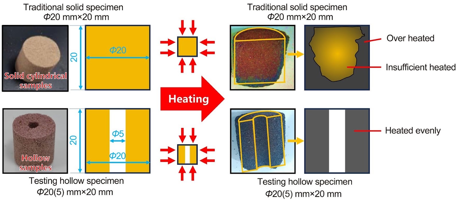
During the casting process, no-bake resin-bonded sand molds and cores rapidly heat up upon contact with high-temperature molten metal, causing dramatic changes in the resin binder system and a significant deterioration in mechanical properties, which subsequently leads to casting defects. To reveal the mechanism behind the evolution of high-temperature performance, the effects of resin content, base sand type, and particle size on the compressive strength of alkaline phenolic no-bake resin-bonded sand at temperatures ranging from 600 °C to 1,000 °C were investigated. The results show that the temperature range of 600-800 °C represents the primary stage of strength loss, corresponding to intense resin decomposition. Meanwhile, structural reorganization of the carbon skeleton above 900 °C can lead to a partial recovery of strength. This study provides key data and theoretical support for understanding the high-temperature mechanical behavior of resin-bonded sand and its relationship with casting defects.

Examine Data & PDF

Frequently Asked Technical Questions (Gallium Nitride & Silicon Carbide)

Q:What is the current scale of China’s 8-inch SiC wafer manufacturing?

Chinese manufacturers including SICC, TankeBlue, and Sanan have certified automotive-grade 8-inch SiC wafers for Tier-1 EV makers, matching global yields from Wolfspeed and STMicroelectronics.

Q:How is China utilizing GaN-on-Diamond technology?

GaN-on-Diamond is primarily researched for extreme heat dissipation in 5G-Advanced and 6G military phased-array communications, where conventional silicon substrates experience thermal choke.

Explore Related Research Pillars in SinoTechIntel