SinoTechIntel Academic Portal
🏛️ Indexed Academic JournalImpact Factor: 3.8

Journal of Semiconductors (半导体学报 - 中国科学院半导体研究所)

Authoritative peer-reviewed journal in materials science, metallurgy, chemistry and engineering technologies: Journal of Semiconductors (半导体学报 - Viện Bán dẫn CAS)

Total Research Papers: 115
Access: 100% Free Open Access
Browse by Publication Year & VolumeReset All Filters ✕

Published Research PapersFiltered: Year 2025 • Vol. 32 • 4

Showing 8 of 115 peer-reviewed papers with full Graphical Abstracts.

Original ResearchVol. 32, Issue 4 • pp. 100-112DOI: 10.1088/1674-4926/25040035Jan 15, 2025

Progress and trends of low-jitter fractional-N PLL

Authors: Jun Yin, Haoran Li, Xiaoqi Lin, Rui P. Martins, Pui-In Mak

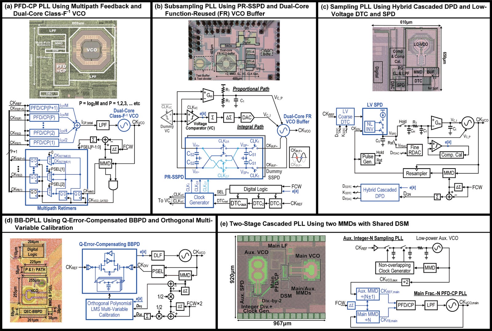
Fractional-N phase-locked loops (PLLs) are widely deployed in high-speed communication systems to generate local oscillator (LO) or clock signals with precise frequency. To support sophisticated modulations for increasing the data rate, the PLL needs to generate low-jitter output. Since the output frequency of the fractional-N PLL is not an integer multiple of the reference clock frequency, the phase error seen by the phase detector (PD) contains not only a random part induced by the oscillator and loop noise, but also a deterministic part due to the fractional operation, which is referred to as the quantization error (Q-error). The Q-error has two side effects on the output jitter. Firstly, the Q-error will induce quantization noise in the PLL output. Although the energy of quantization noise can be shaped to high offset frequencies and suppressed by the low-pass characteristics of the loop with the aid of a delta-sigma modulator (DSM), it could still contribute a substantial portion of the output jitter if a moderate or large loop bandwidth is required to suppress the oscillator's phase noise (PN). Secondly, when the Q-error passes through a nonlinear PD, fractional spurs will be generated, and quantization noise at high offset frequencies will be folded into in-band, which also degrades the output jitter. These side effects could limit the jitter performance in fractional-N PLLs. In the following sections, recent techniques to minimize the side effects of Q-error that enable low-jitter fractional-N PLL with high power efficiency will be reviewed.
Progress and trends of low-jitter fractional-N PLL
Graphical Abstract
Original ResearchVol. 32, Issue 4 • pp. 100-112DOI: 10.1088/1674-4926/25040026Jan 15, 2025

A γ-irradiated AlGaN/GaN Schottky barrier diode with barrier-decreased Schottky junction and high breakdown voltage

Authors: CHEN Jiahao, ZHANG Tao, TAO Ziqi, SU Kai, XU Shengrui, LI Xiangdong, SU Huake, ZHANG Yachao, HAO Yue, ZHANG Jincheng

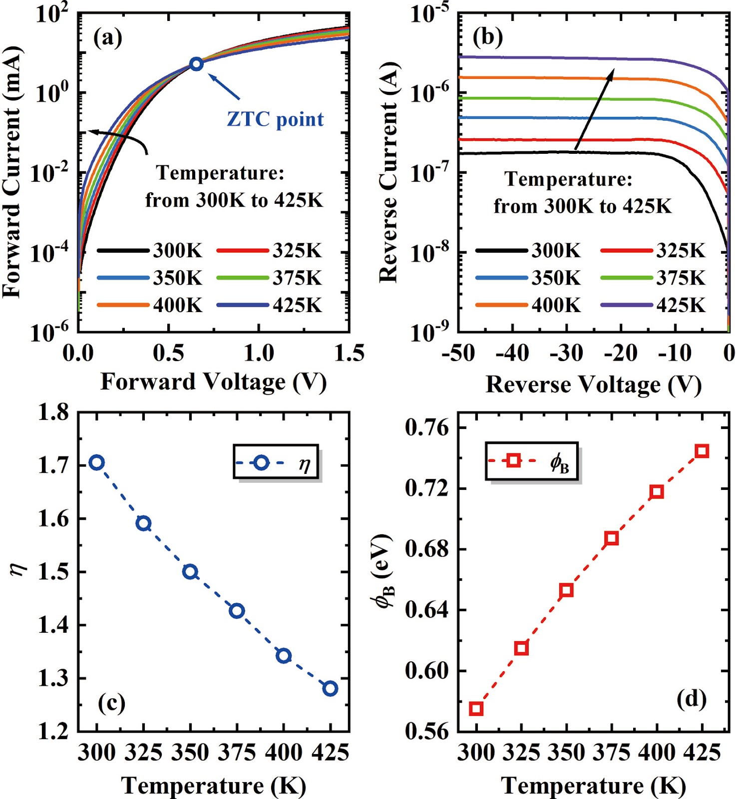
In this letter, we demonstrate the effect of γ irradiation on the lateral AlGaN/GaN Schottky barrier diodes (SBDs) with self-terminated recessed anode structure and low work-function metal tungsten (W) as anode. For a comprehensive evaluation of the radiation-resistance performance of the device, the total dose of γ irradiation is up to 100 kGy with irradiation time of 20 h. Attributed to the barrier lowering effect of the W/GaN interface induced by γ irradiation observed in the experiment, the extracted turn-on voltage (VON) defined at anode forward current of 1 mA decreases from 0.47 to 0.43 V. Meanwhile, benefiting from the reinforced Schottky interface treated by post-anode-annealing, a high breakdown voltage (BV) of 1.75 kV is obtained for the γ-irradiated AlGaN/GaN SBD, which shows the promising application for the deep-space radiation environment and promotes the development of radiation-resistance research for GaN SBDs.

A γ-irradiated AlGaN/GaN Schottky barrier diode with barrier-decreased Schottky junction and high breakdown voltage
Graphical Abstract
Original ResearchVol. 32, Issue 4 • pp. 100-112DOI: 10.1088/1674-4926/25040037Jan 15, 2025

Trends and emerging techniques in isolated power converters

Authors: Lin Cheng, Dongfang Pan

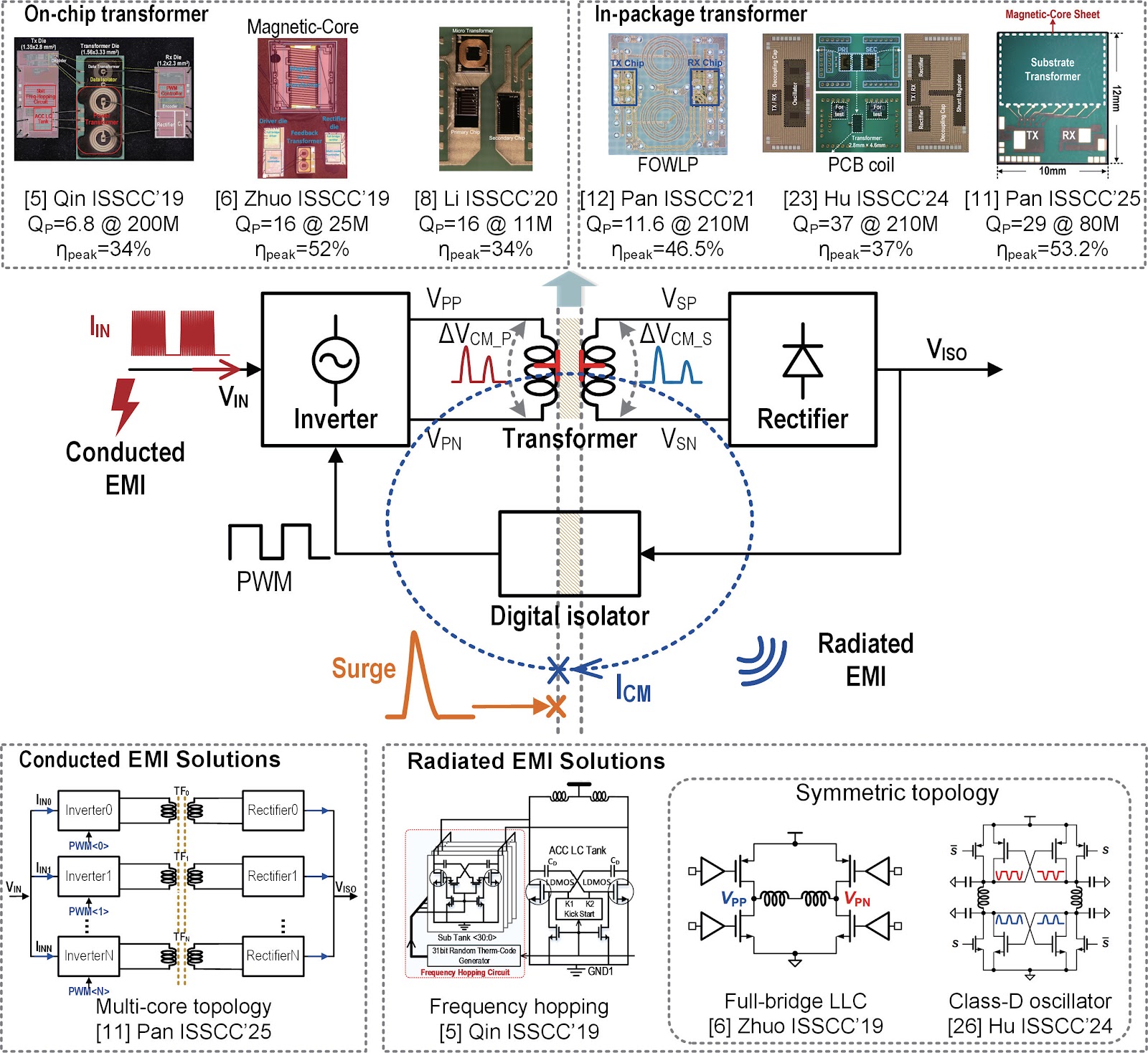
Isolated power converters have emerged as an active research topic in power integrated circuit (IC) design. Reflecting this growing interest, ISSCC 2025 has featured a dedicated session on "Isolated Power and Gate Drivers". These converters enable safe and reliable power delivery across voltage domains and are widely used in renewable energy, electric vehicles, and telecommunications. Galvanic isolation prevents surge currents and ground loop issues in harsh high-voltage environments. As demand grows for compact, efficient, and high–power-density solutions, fully integrated architectures featuring on-chip transformers are increasingly favored over traditional module-based designs, offering >5 kV isolation with a smaller footprint and lower system cost. This mini review highlights recent advances and trends in isolated power converter technologies, focusing on efficiency improvement and EMI suppression.

Trends and emerging techniques in isolated power converters
Graphical Abstract
Original ResearchVol. 32, Issue 4 • pp. 100-112DOI: 10.1088/1674-4926/25040033Jan 15, 2025

Multi-chip multi-phase DC−DC converters for AI power: a ring, a chain, or a net, independent or master-slave?

Authors: Yan Lu, Zhiguo Tong, Jiacheng Yang, Zhewen Yu, Mo Huang, Xiangyu Mao

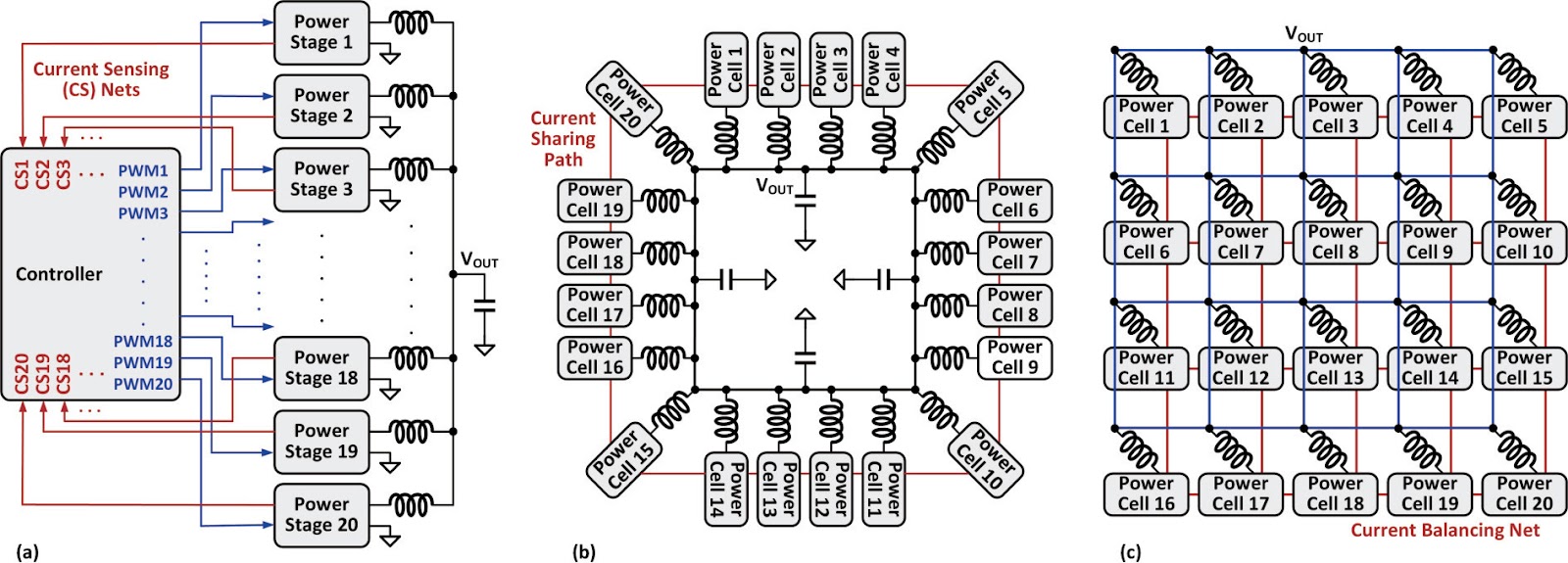
As artificial intelligence (AI) workloads escalate exponentially, ultra-thin, high-efficiency voltage regulator modules (VRMs) with exceptional power density become essential for backside-mounted configurations. High-density multiphase DC−DC converters are pivotal for implementing vertical power delivery (VPD) architectures in XPU platforms. Strategically positioning these converters beneath processors and maximizing spatial utilization enables core rail currents exceeding 2 kA while significantly reducing power distribution network (PDN) losses compared to conventional solutions. The VPD configuration elevates system-level energy efficiency with >100 W power saving per processor, yielding megawatt-scale savings in a datacenter that uses ~100 000 processors. The synergy of 48 V power conversion architectures and advanced packaging techniques enables the industry’s commitment to balancing computational demands with CO2 emission reduction and environmental sustainability. This paper discusses system architecture, layout geometry, and control strategies for multi-chip multi-phase DC−DC converters, comparing ring, chain, and net topologies, as well as independent and master-slave control schemes.

Multi-chip multi-phase DC−DC converters for AI power: a ring, a chain, or a net, independent or master-slave?
Graphical Abstract
Original ResearchVol. 32, Issue 4 • pp. 100-112DOI: 10.1088/1674-4926/25040013Jan 15, 2025

Eco-sustainable biosynthesis of CoFe2O4 nanoparticles using apple extract for multifunctional applications

Authors: Heba Hussein, Sobhy Sayed Ibrahim, Sherif Ahmed Khairy

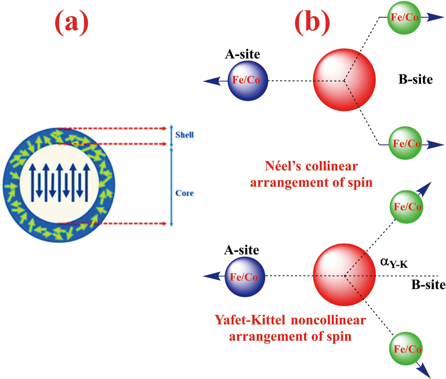
This study investigates the effect of apple extract on CoFe2O4 nanoparticles synthesized via a green self-ignition method. High resolution transmission electron microscope (HRTEM) showed nanometric particles with varied shapes, while X-ray diffraction (XRD) and Rietveld refinement confirmed a facecentered cubic (Fd3̅m) structure. Mössbauer spectroscopy revealed a Zeeman sextet pattern with only Fe3+ ions. Ultra violet vissible nearinfrared (UV–Vis–NIR) spectra indicated strong absorbance in the visible and NIR regions, suggesting optoelectronic potential. The nanoparticles demonstrated high photo-Fenton catalytic efficiency, degrading 96.88% of Methylene Blue under visible light. They also exhibited 100% adsorption capacities for Cr3+ and Pb2+, making them effective for water treatment. These properties were attributed to a large surface area (347.04 m2/g), mesoporous structure, and mixed spinel phase. ANOVA and Tukey’s honestly significant difference (HSD) tests confirmed that contact time and adsorbent dosage significantly affected pollutant removal. Additionally, strong antimicrobial activity highlighted their biotechnological relevance. The inclusion of apple extract enhanced structural and functional features, expanding application prospects in spin valves, magnetic recording, refrigeration, microwave technologies (C to Ku bands), optoelectronics, and biotechnology. Future work should explore the photo-Fenton degradation mechanism and optimize synthesis for scalable production, aiming to maximize their industrial utility.

Eco-sustainable biosynthesis of CoFe2O4 nanoparticles using apple extract for multifunctional applications
Graphical Abstract
Original ResearchVol. 32, Issue 4 • pp. 100-112DOI: 10.1088/1674-4926/25040027Jan 15, 2025

Solar-blind UV light-modulated β-Ga2O3 full-wave bridge rectifier

Authors: Haifeng Chen, Yuduo Zhang, Xiexin Sun, Jingguo Zong, Qin Lu, Yifan Jia, Zhenfu Feng, Zhan Wang, Lijun Li, Xiangtai Liu, Shaoqing Wang, Yue Hao

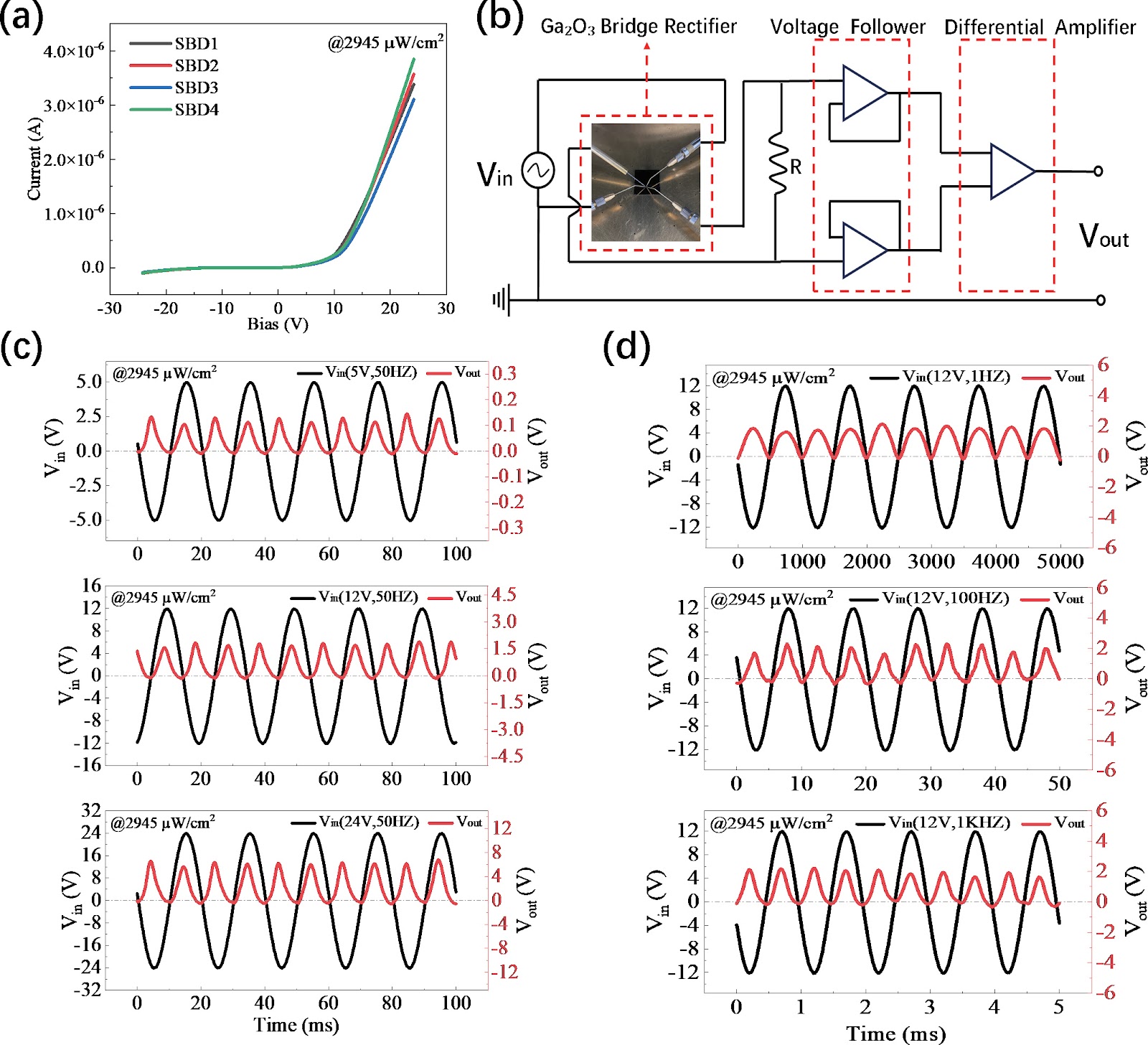
A monolithic integrated full-wave bridge rectifier consisted of horizontal Schottky-barrier diodes (SBD) is prepared based on 100 nm ultra-thin β-Ga2O3 and demonstrated the solar-blind UV (SUV) light-modulated characteristics. Under SUV light illumination, the rectifier has the excellent full-wave rectification characteristics for the AC input signals of 5, 12, and 24 V with different frequencies. Further, experimental results confirmed the feasibility of continuously tuning the rectified output through SUV light-encoding. This work provides valuable insights for the development of optically programmable Ga2O3 AC-DC converters.

Solar-blind UV light-modulated β-Ga2O3 full-wave bridge rectifier
Graphical Abstract
Original ResearchVol. 32, Issue 4 • pp. 100-112DOI: 10.1088/1674-4926/25040012Jan 15, 2025

A minireview on technology and application of silicon integrated single crystal perovskite

Authors: Jing Weng, Molang Cai, Xu Pan, Xing Li

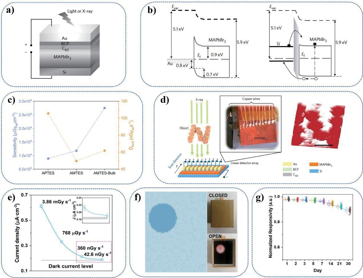
Metal halide perovskites (MHPs) have become promising optoelectronic materials due to their long carrier lifetimes and high mobility. However, the presence of defects and ion migration in MHPs results in high and unstable dark currents, which compromise the stability and detection performance of MHP-based optoelectronic devices. Interfacial engineering has proven to be an effective strategy to reduce defect density in MHPs and suppress ion migration. Given the compatibility of silicon (Si) and MHP processing technologies, coupled with the simplicity and cost-effectiveness of the approach, the integration of MHPs onto Si surfaces has become a prominent area of research. This integration not only enhances device performance but also expands their practical applications. This review provides an overview of the integration technologies for Si and single crystal MHPs, evaluates the advantages and limitations of various integration schemes (including inverse temperature crystallization, vacuum-assisted vapor deposition, and anti-solvent vapor-assisted crystallization), and explores the practical applications of Si/MHP-integrated optoelectronic devices with different structures. These optimized devices exhibit outstanding performance in X-ray detection, multi-wavelength photodetection, and circularly polarized light detection. This review provides a systematic reference for technological innovation and application expansion of Si/MHP-integrated devices.

A minireview on technology and application of silicon integrated single crystal perovskite
Graphical Abstract
Original ResearchVol. 32, Issue 4 • pp. 100-112DOI: 10.1088/1674-4926/25040023Jan 15, 2025

Radiation hardness of 1.2 kV SiC power devices with advanced edge termination structures under proton irradiation

Authors: Sangyeob Kim, Jeongtae Kim, Dong-Seok Kim, Hyuncheol Bae, Min-Woo Ha, Ogyun Seok

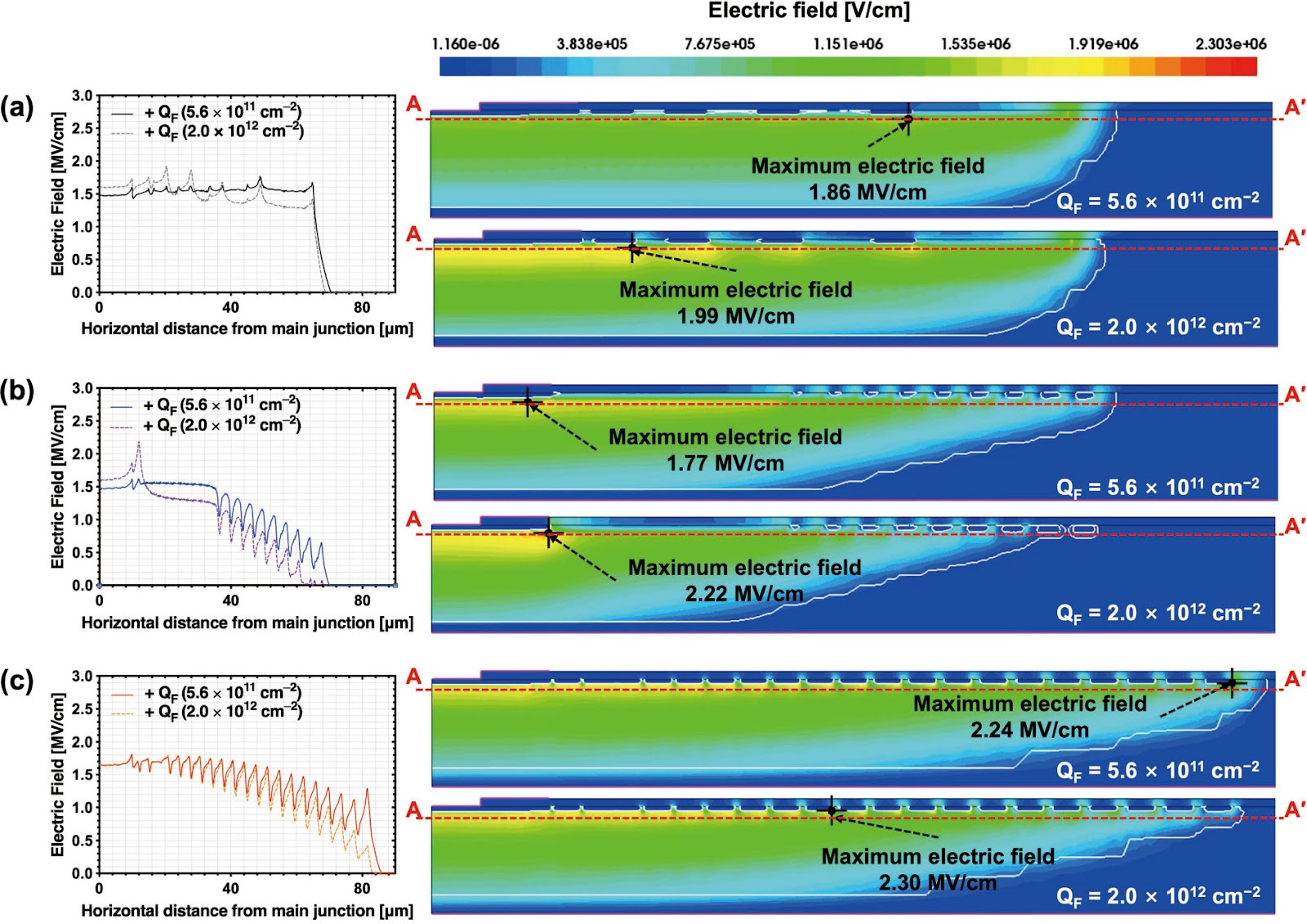
This work presents a systematic analysis of proton-induced total ionizing dose (TID) effects in 1.2 kV silicon carbide (SiC) power devices with various edge termination structures. Three edge terminations including ring-assisted junction termination extension (RA-JTE), multiple floating zone JTE (MFZ-JTE), and field limiting rings (FLR) were fabricated and irradiated with 45 MeV protons at fluences ranging from 1 × 10^12 to 1 × 10^14 cm^-2. Experimental results, supported by TCAD simulations, show that the RA-JTE structure maintained stable breakdown performance with less than 1% variation due to its effective electric field redistribution by multiple P+ rings. In contrast, MFZ-JTE and FLR exhibit breakdown voltage shifts of 6.1% and 15.2%, respectively, under the highest fluence. These results demonstrate the superior radiation tolerance of the RA-JTE structure under TID conditions and provide practical design guidance for radiation-hardened SiC power devices in space and other high-radiation environments.

Radiation hardness of 1.2 kV SiC power devices with advanced edge termination structures under proton irradiation
Graphical Abstract