SinoTechIntel Academic Portal
🏛️ Indexed Academic JournalImpact Factor: 3.8

Journal of Semiconductors (半导体学报 - 中国科学院半导体研究所)

Authoritative peer-reviewed journal in materials science, metallurgy, chemistry and engineering technologies: Journal of Semiconductors (半导体学报 - Viện Bán dẫn CAS)

Total Research Papers: 115
Access: 100% Free Open Access
Browse by Publication Year & VolumeReset All Filters ✕

Published Research PapersFiltered: Year 2025 • Vol. 32 • 3

Showing 15 of 115 peer-reviewed papers with full Graphical Abstracts.

Original ResearchVol. 32, Issue 3 • pp. 100-112DOI: 10.1088/1674-4926/25030009Jan 15, 2025

Self-assembled flexible Ti3C2Tx MXene-based thermally chargeable supercapacitor

Authors: Lifeng Wu, La Li, Guozhen Shen

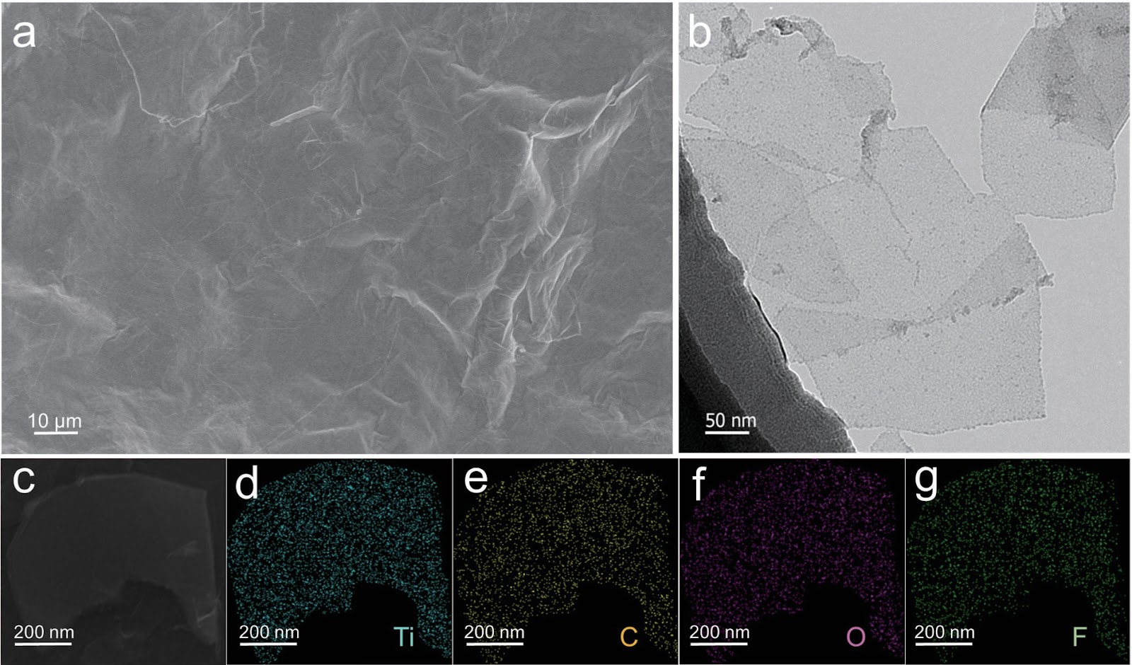
Thermally chargeable supercapacitors (TCSCs) have unique advantages in the collection, conversion, and storage of thermal energy, contributing to the development of new strategies for thermal energy utilization. 2D MXene materials are predicted to be highly promising new thermoelectric materials. Here, we report a self-assembled flexible Ti3C2Tx MXene-based TCSC device, using prepared Ti3C2Tx MXene as the capacitor electrode and a NaClO4/PEO gel as the electrolyte. We also explore the working mechanism of the TCSCs. The fabricated Ti3C2Tx-based TCSCs exhibit an excellent Seebeck coefficient of 11.8 mV∙K−1 on average and maintain good cycling stability under various temperature differences. Demonstrations of multiple practical applications show that Ti3C2Tx MXene-based TCSC devices are excellent candidates for self-powered integrated electronic devices.
Self-assembled flexible Ti3C2Tx MXene-based thermally chargeable supercapacitor
Graphical Abstract
Original ResearchVol. 32, Issue 3 • pp. 100-112DOI: 10.1088/1674-4926/25030023Jan 15, 2025

Nucleation control for the growth of two-dimensional single crystals

Authors: Jinxia Bai, Chi Zhang, Fankai Zeng, Jinzong Kou, Jinhuan Wang, Xiaozhi Xu

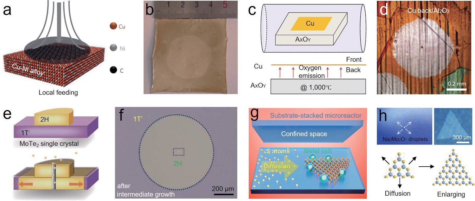
The unique structure and exceptional properties of two-dimensional (2D) materials offer significant potential for transformative advancements in semiconductor industry. Similar to the reliance on wafer-scale single-crystal ingots for silicon-based chips, practical applications of 2D materials at the chip level need large-scale, high-quality production of 2D single crystals. Over the past two decades, the size of 2D single-crystals has been improved to wafer or meter scale, where the nucleation control during the growth process is particularly important. Therefore, it is essential to conduct a comprehensive review of nucleation control to gain fundamental insights into the growth of 2D single-crystal materials. This review mainly focuses on two aspects: controlling nucleation density to enable the growth from a single nucleus, and controlling nucleation position to achieve the unidirectionally aligned islands and subsequent seamless stitching. Finally, we provide an overview and forecast of the strategic pathways for emerging 2D materials.

Nucleation control for the growth of two-dimensional single crystals
Graphical Abstract
Original ResearchVol. 32, Issue 3 • pp. 100-112DOI: 10.1088/1674-4926/25030003Jan 15, 2025

Synthesis of p-type PbS quantum dot ink via inorganic ligand exchange in solution for high-efficiency and stable solar cells

Authors: Napasuda Wichaiyo, Yuyao Wei, Chao Ding, Guozheng Shi, Witoon Yindeesuk, Liang Wang, Huān Bì, Jiaqi Liu, Shuzi Hayase, Yusheng Li, Yongge Yang, Qing Shen

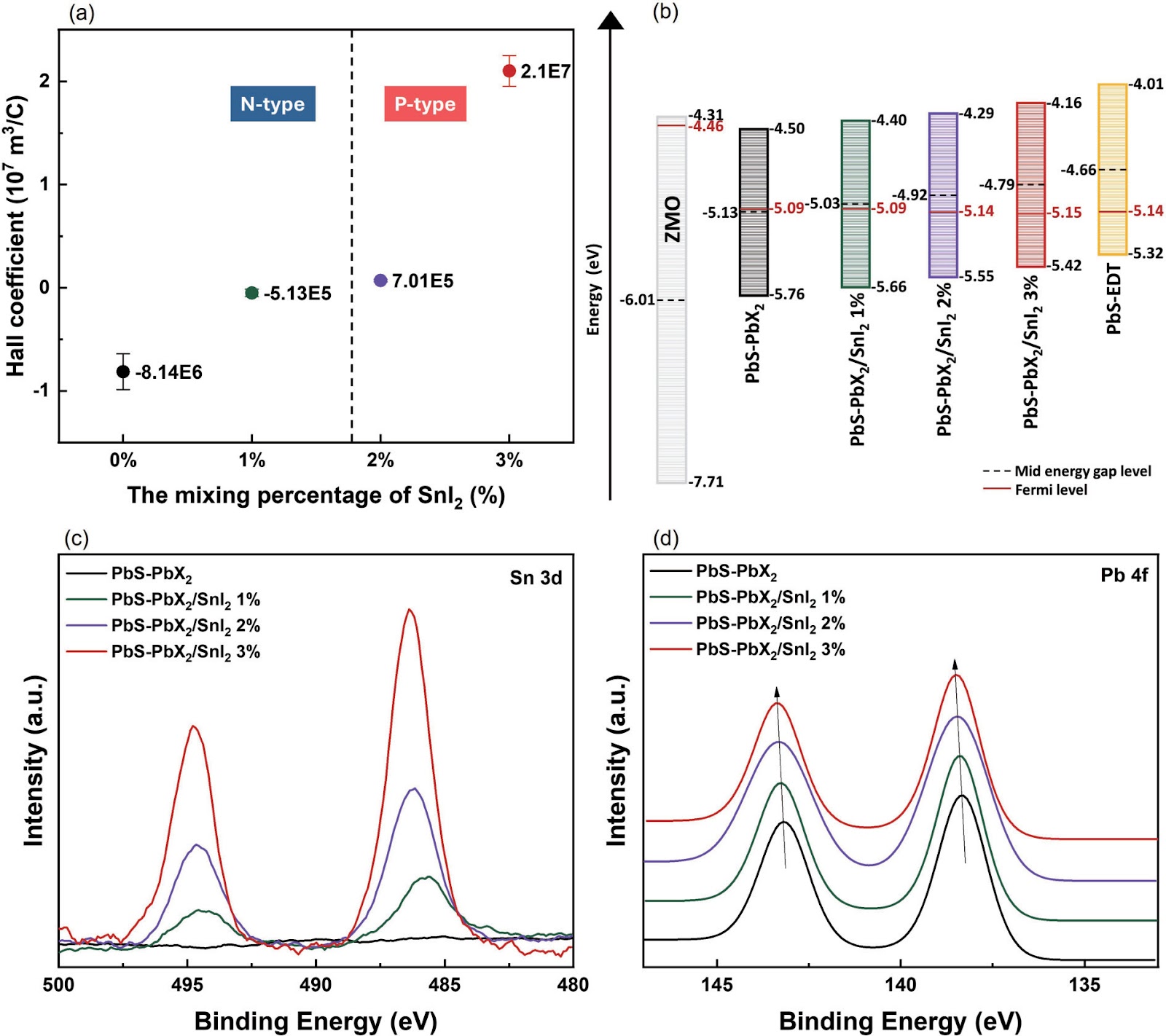
Traditional p-type colloidal quantum dot (CQD) hole transport layers (HTLs) used in CQD solar cells (CQDSCs) are commonly based on organic ligands exchange and the layer-by-layer (LbL) technique. Nonetheless, the ligand detachment and complex fabrication process introduce surface defects, compromising device stability and efficiency. In this work, we propose a solution-phase ligand exchange (SPLE) method utilizing inorganic ligands to develop stable p-type lead sulfide (PbS) CQD inks for the first time. Various amounts of tin (II) iodide (SnI2) were mixed with lead halide (PbX2; X = I, Br) in the ligand solution. By precisely controlling the SnI₂ concentration, we regulate the transition of PbS QDs from n-type to p-type. PbS CQDSCs were fabricated using two different HTL approaches: one with 1,2-ethanedithiol (EDT)-passivated QDs via the LbL method (control) and another with inorganic ligand-passivated QD ink (target). The target devices achieved a higher power conversion efficiency (PCE) of 10.93%, compared to 9.83% for the control devices. This improvement is attributed to reduced interfacial defects and enhanced carrier mobility. The proposed technique offers an efficient pathway for producing stable p-type PbS CQD inks using inorganic ligands, paving the way for high-performance and flexible CQD-based optoelectronic devices.

Synthesis of p-type PbS quantum dot ink via inorganic ligand exchange in solution for high-efficiency and stable solar cells
Graphical Abstract
Original ResearchVol. 32, Issue 3 • pp. 100-112DOI: 10.1088/1674-4926/25030012Jan 15, 2025

Manipulation strategy of cation inhomogeneity in perovskite solar cells

Authors: Jiale Sun, Xuxia Shai, Weitao Chen, Shenchao Li, Jinlan He, Xinxing Liu, Dongmei He, Yue Yu, Jiangzhao Chen

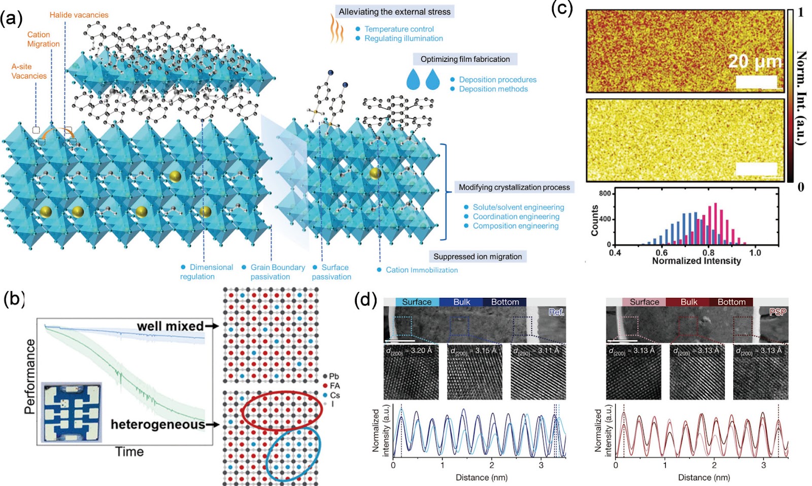
In recent years, research advancements have highlighted the critical role of the A-site cation in determining the optoelectronic and physicochemical properties of organic–inorganic lead halide perovskites. Mixed-cation perovskites (MCPs) have been extensively used as absorber thin films in perovskite solar cells (PSCs), achieving high power conversion efficiencies (PCE) over 26%. The incorporation of mixed cations has led to a more optimal tolerance factor for the crystal structure, enhancing structural stability and providing additional functionalities to improve the chemical stability of the absorber thin films. However, mixed-cation perovskite absorbers often experience element and phase segregation, which can reduce device efficiency and operational lifespan. This segregation is a widespread phenomenon observed across various types of MCPs, whether in 2D or 3D structures. Therefore, understanding the fundamental causes of non-uniformity and phase segregation, as well as effective nanoscale regulatory strategies, is essential for enhancing the performance of PSCs. The development of high-quality MCPs with highly uniform cation distribution and stable phases is critical for addressing the stability challenges in PSCs.

Manipulation strategy of cation inhomogeneity in perovskite solar cells
Graphical Abstract
Original ResearchVol. 32, Issue 3 • pp. 100-112DOI: 10.1088/1674-4926/25030001Jan 15, 2025

A 112 Gbps DSP-based PAM4 SerDes receiver with a wide band equalization tuning AFE in 7 nm FinFET

Authors: Huanan Guo, Yufeng Yao, Jiazhen Ni, Xiang Gao

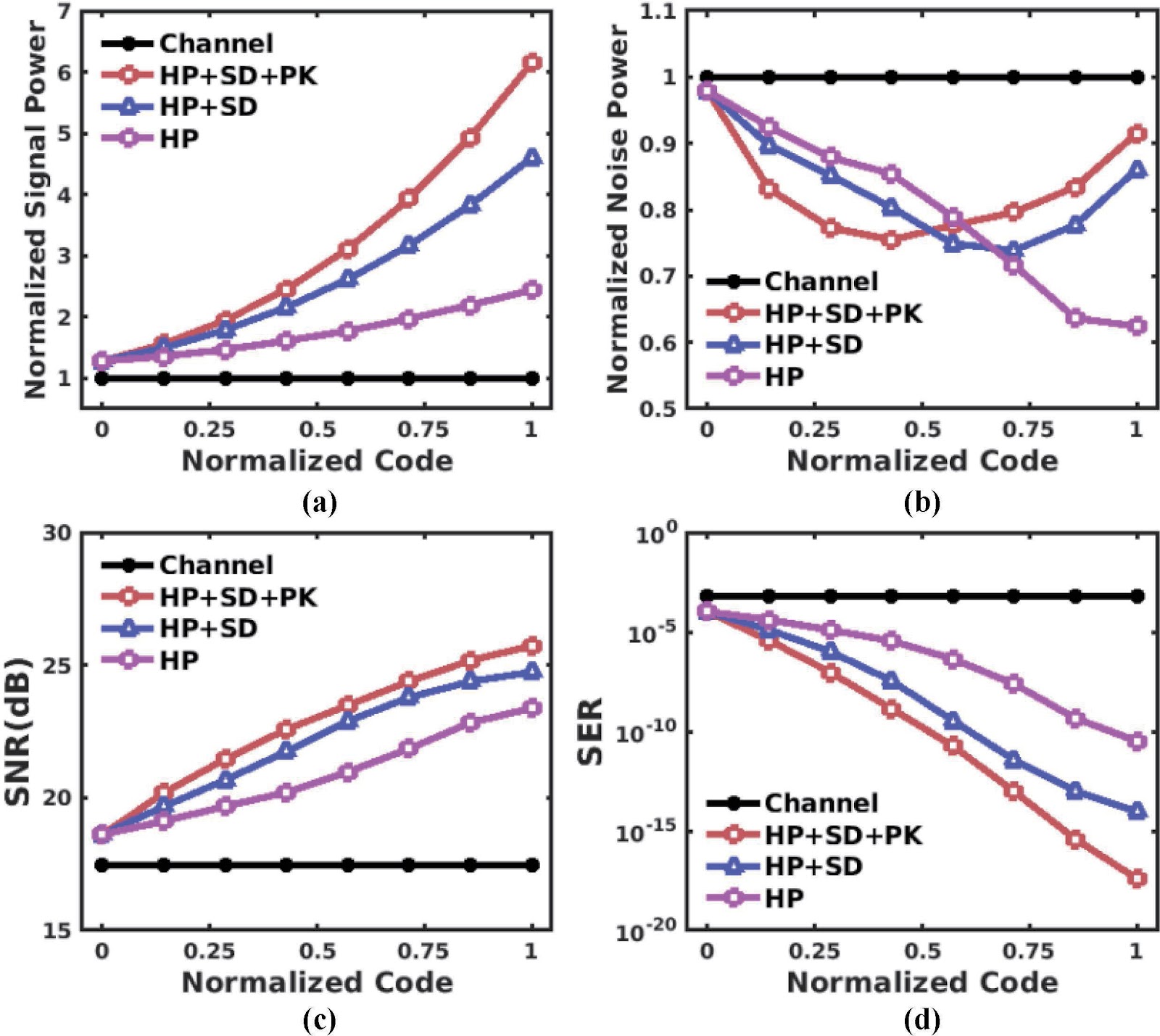
In DSP-based SerDes application, it is essential for AFE to implement a pre-ADC equalization to provide a better signal for ADC and DSP. To meet the various equalization requirements of different channel and transmitter configurations, this paper presents a 112 Gbps DSP-Based PAM4 SerDes receiver with a wide band equalization tuning AFE. The AFE is realized by implementing source degeneration transconductance, feedforward high-pass branch and inductive feedback peaking TIA. The AFE offers a flexible equalization gain tuning of up to 17.5 dB at Nyquist frequency without affecting the DC gain. With the proposed AFE, the receiver demonstrates eye opening after digital FIR equalization and achieves 6 × 10⁻⁹ BER with a 29.6 dB insertion loss channel.

A 112 Gbps DSP-based PAM4 SerDes receiver with a wide band equalization tuning AFE in 7 nm FinFET
Graphical Abstract
Original ResearchVol. 32, Issue 3 • pp. 100-112DOI: 10.1088/1674-4926/25030025Jan 15, 2025

CZTS based novel bifunctional photovoltaic and self-powered photodetection nano system

Authors: Kalyan B. Chavan, Maruti V. Salve, Shweta Chaure, Nandu B. Chaure

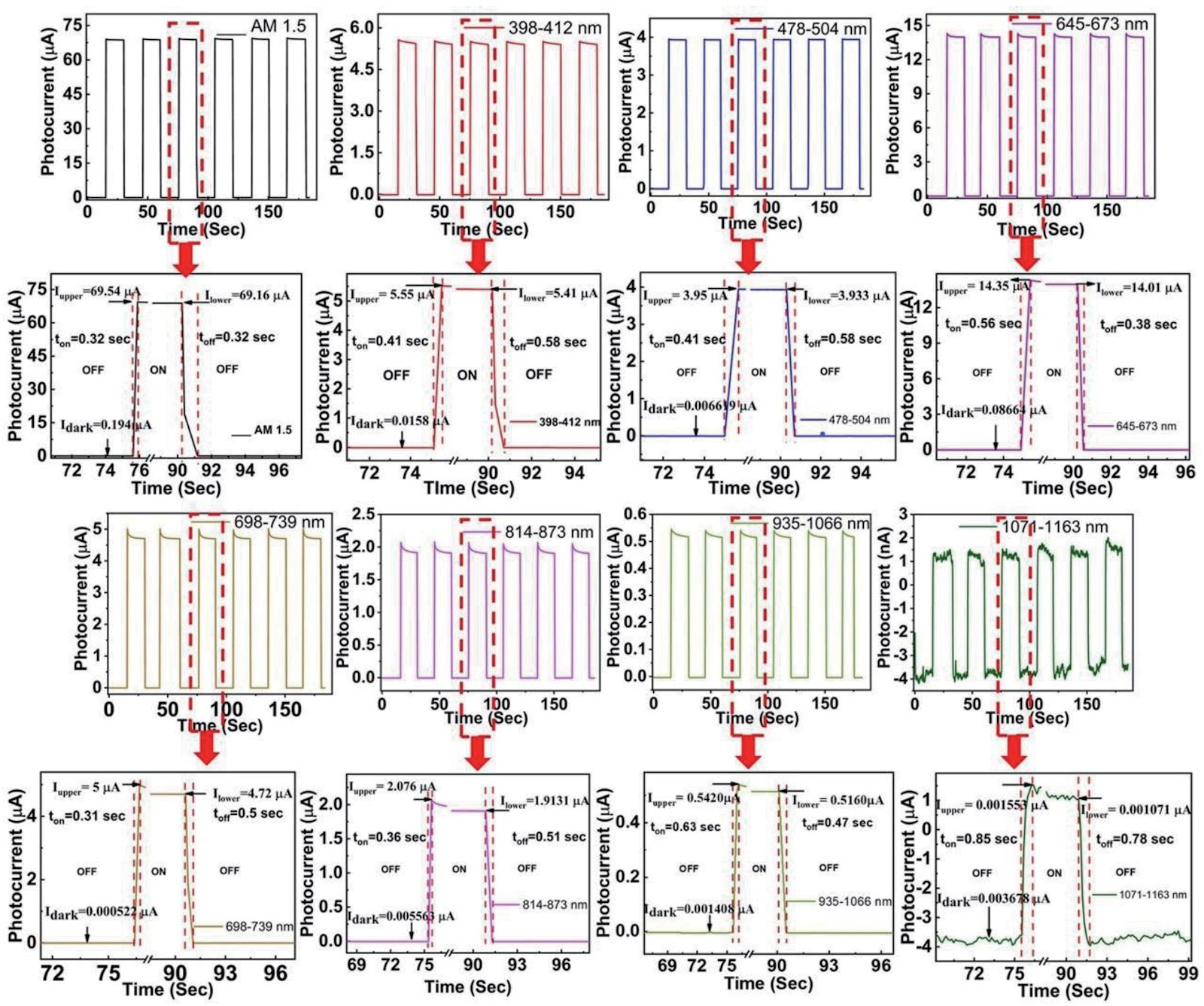
CZTS (Cu2ZnSnS4) is a quaternary semiconductor that is environmentally friendly, less expensive. In this paper, we report on the optimization and fabrication of CZTS-based heterojunction nanodevices for bifunctional applications such as solar cells and photodetectors. CZTS thin films were deposited on top of (Molybdenum) Mo-coated glass substrates via RF sputtering at 100 and 200 W. Rapid thermal processing (RTP) was used at 300, 400, and 500 °C temperatures. CdS (cadmium sulphide) was deposited on CZTS using a chemical bath deposition system with 3- and 5-min deposition times. ZnO (zinc oxide) and AZO (aluminium doped zinc oxide) layers were deposited using RF (radio frequency) sputtering to create the solar device. XRD confirms the formation of a tetragonal structure with increased crystallinity due to the use of RTP. Raman reveals the characteristic Raman shift peak associated with CZTS at 336 and 335 cm−1. The FESEM shows a relationship with RTP temperature. Surface features, including grain size, vary with RTP temperature. The ideality factor is nearly 2, indicating imperfection in the Mo/CZTS interface. Schottky barrier height estimates range from 0.6 to 0.7 eV. Absorbance and transmittance show a predictable fluctuation with RTP temperature. Photovoltaic device was built using the higher crystalline feature of CZTS in conjunction with CdS deposited at 3 and 5 min. The efficiency of CdS deposited after 3 and 5 min was 1.15 and 0.97 percent, respectively. Fabricated devices were used for wavelength-dependent photodetection. This work demonstrated self-powered photodetection.

CZTS based novel bifunctional photovoltaic and self-powered photodetection nano system
Graphical Abstract
Original ResearchVol. 32, Issue 3 • pp. 100-112DOI: 10.1088/1674-4926/25030041Jan 15, 2025

Effect of nitrogen incorporation and surface passivation on photoluminescence properties of InAs-based nanowires

Authors: Ratmir Ustimenko, Danila Karaulov, Maxim Vinnichenko, Ilya Norvatov, Andrey Kaveev, Vladimir Fedorov, Ivan Mukhin, Dmitry Firsov

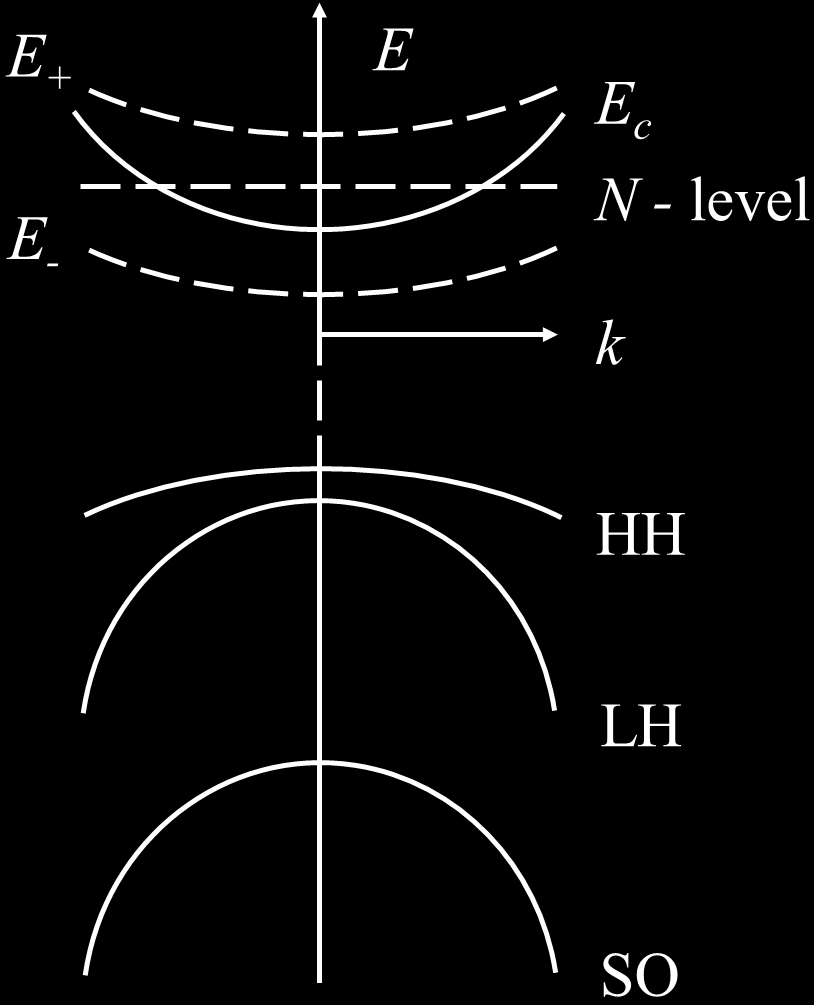
InAsN nanowires on InAs stems were obtained using plasma-assisted molecular beam epitaxy on a SiOx/Si (111) substrate. Also, heterostructured InAs/InAsN and InAsN/InP nanowires were grown in the core/shell geometry. In the low-temperature photoluminescence spectra of the grown structures, spectral features are observed that correspond to the polytypic structure of nanowires with a predominance of the wurtzite phase and parasitic islands of the sphalerite phase. It was shown that the interband photoluminescence spectral features of InAsN nanowires experience a red shift relative to the pristine InAs nanowires. The incorporation of nitrogen reduces the bandgap by splitting the conduction band into two subbands. The position of the spectral features in the photoluminescence spectra confirms the formation of a nitride solid solution with a polytypic hexagonal structure, having a concentration of nitrogen atoms of up to 0.7%. Additional passivation of the nanowire surface with InP leads to a decrease in the intensity of nonradiative recombination and an improvement in the photoluminescent response of the nanowires, which makes it possible to detect photoluminescence emission at room temperature. Thus, by changing the composition and morphology of nanowires, it is possible to control their electronic structure, which allows varying the operating range of detectors and mid-IR radiation sources based on them.

Effect of nitrogen incorporation and surface passivation on photoluminescence properties of InAs-based nanowires
Graphical Abstract
Original ResearchVol. 32, Issue 3 • pp. 100-112DOI: 10.1088/1674-4926/25030801Jan 15, 2025

Preface to Special Topic on Quantum Dot Semiconductor Optoelectronic Materials, Devices, and Characterization

Authors: Zeke Liu, Wanli Ma

The discovery and synthesis of colloidal quantum dots (QDs) were awarded the 2023 Nobel Prize in Chemistry. QDs, as a novel class of materials distinct from traditional molecular materials and bulk materials, have rapidly emerged in the field of optoelectronic applications due to their unique size-, composition-, surface-, and process-dependent optoelectronic properties. More importantly, their ultra-high specific surface area allows for the application of various surface chemical engineering techniques to regulate and optimize their optoelectronic performance. Furthermore, three-dimensionally confined QDs can achieve nearly perfect photoluminescence quantum yields and extended hot carrier cooling times. Particularly, their ability to be colloidally synthesized and processed using industrially friendly solvents is driving transformative changes in the fields of electronics, photonics, and optoelectronics. In this Special Topic, we have selected four typical types of QD materials and their optoelectronic applications, including 4 Research Articles and 1 Review, to introduce the latest research advances in QD materials and optoelectronic fields.

Preface to Special Topic on Quantum Dot Semiconductor Optoelectronic Materials, Devices, and Characterization
Graphical Abstract
Original ResearchVol. 32, Issue 3 • pp. 100-112DOI: 10.1088/1674-4926/25030015Jan 15, 2025

High-speed electro-absorption modulated laser

Authors: Zhenyao Li, Chen Lyu, Xuliang Zhou, Mengqi Wang, Haotian Qiu, Yejin Zhang, Hongyan Yu, Jiaoqing Pan

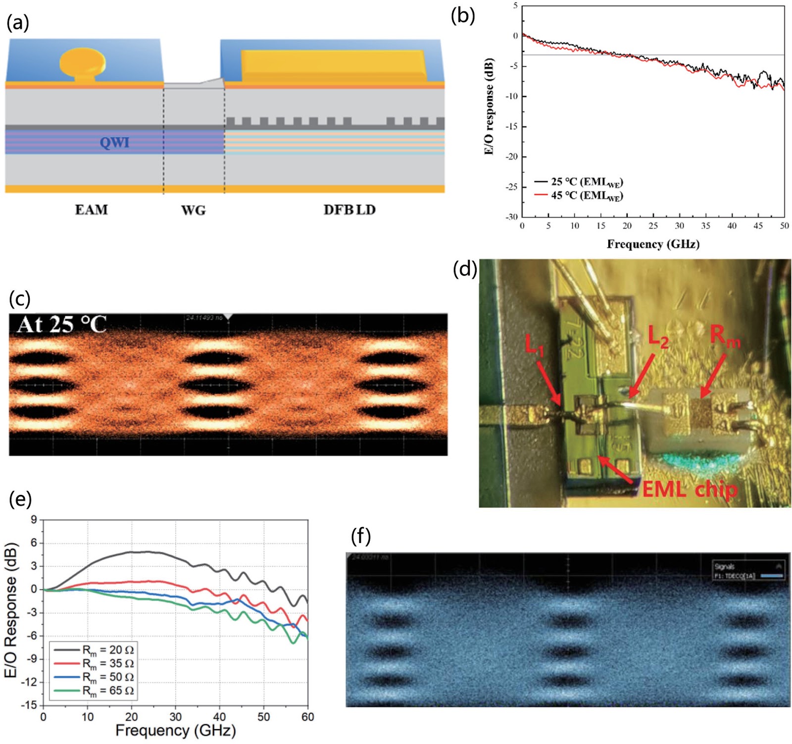
Currently, the global 5G network, cloud computing, and data center industries are experiencing rapid development. The continuous growth of data center traffic has driven the vigorous progress in high-speed optical transceivers for optical interconnection within data centers. The electro-absorption modulated laser (EML), which is widely used in optical fiber communications, data centers, and high-speed data transmission systems, represents a high-performance photoelectric conversion device. Compared to traditional directly modulated lasers (DMLs), EMLs demonstrate lower frequency chirp and higher modulation bandwidth, enabling support for higher data rates and longer transmission distances. This article introduces the composition, working principles, manufacturing processes, and applications of EMLs. It reviews the progress on advanced indium phosphide (InP)-based EML devices from research institutions worldwide, while summarizing and comparing data transmission rates and key technical approaches across various studies.

High-speed electro-absorption modulated laser
Graphical Abstract
Original ResearchVol. 32, Issue 3 • pp. 100-112DOI: 10.1088/1674-4926/25030031Jan 15, 2025

Jitter suppression scheme for detection pulses in high-speed sinusoidal gated single-photon detectors

Authors: Lianjun Jiang, Dongdong Li, Dawei Li, Yuqiang Fang, Ming Liu, Wei Jiang, Zhilin Xie, Guoqing Liu, Rui Ma, Yukang Zhao, Jian Sun, Lei Chang, Lin Yu, Shibiao Tang

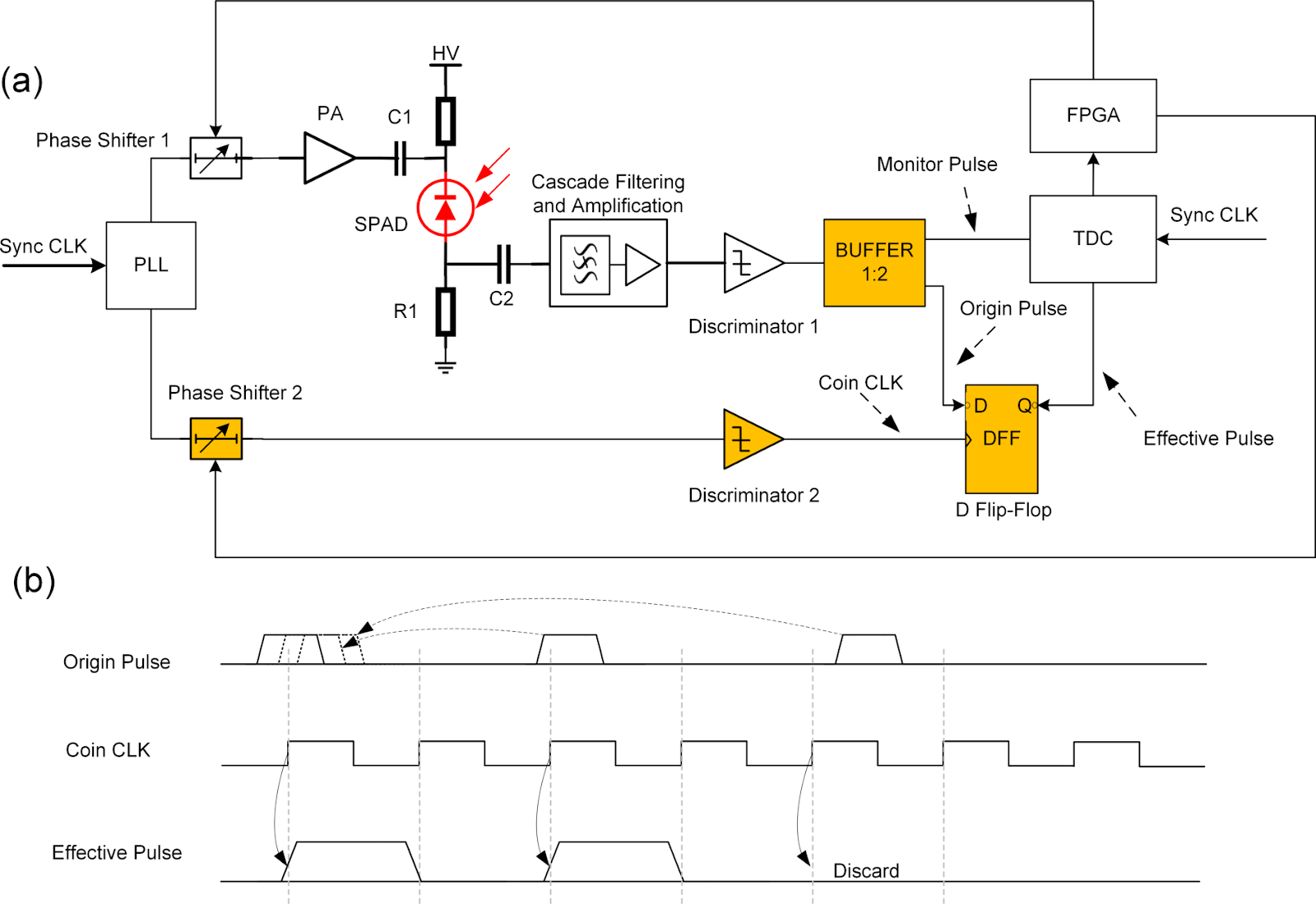
Quantum key distribution (QKD) achieves information-theoretic security based on quantum mechanics principles, where single-photon detectors (SPDs) serve as critical components. This study focuses on the sinusoidal gated SPDs widely used in high-speed QKD systems. We investigate the mechanisms underlying the rising-edge jitter in detection signals, identifying contributions from factors such as the temporal width of injected optical pulses, avalanche generation processes, avalanche signal extraction, and pulse discrimination. To address the issue of excessive jitter-induced bit errors, we propose a retiming scheme that utilizes coincidence signals synchronized with the sinusoidal gating signal. This approach effectively suppresses detection signal jitter and reduces the after-pulse probability of the detector. Experimental validation using a high-precision time-to-digital converter (TDC) demonstrates a significant reduction in the rising-edge jitter distribution after applying the suppression scheme. The proposed method features clear principles and straightforward engineering implementation, avoiding direct interference with the detector's operational processes. The designed high-speed sinusoidal gated InGaAs/InP SPD operates at 1.25 GHz, achieving a remarkable reduction in after-pulse probability from 10.7% (without jitter suppression) to 0.72%, thereby enhancing the overall performance of QKD systems.

Jitter suppression scheme for detection pulses in high-speed sinusoidal gated single-photon detectors
Graphical Abstract
Original ResearchVol. 32, Issue 3 • pp. 100-112DOI: 10.1088/1674-4926/25030011Jan 15, 2025

Research on optical soliton characteristics GaSb-based ~2 μm wavelength two-section integrated optical chip

Authors: Wenjun Yu, Zhongliang Qiao, Xiang Li, Jia Xu Brian Sia, Dengqun Weng, Xiaohu Hou, Zaijin Li, Lin Li, Hao Chen, Zhibin Zhao, Yi Qu, Chongyang Liu, Hong Wang, Yu Zhang, Zhichuan Niu

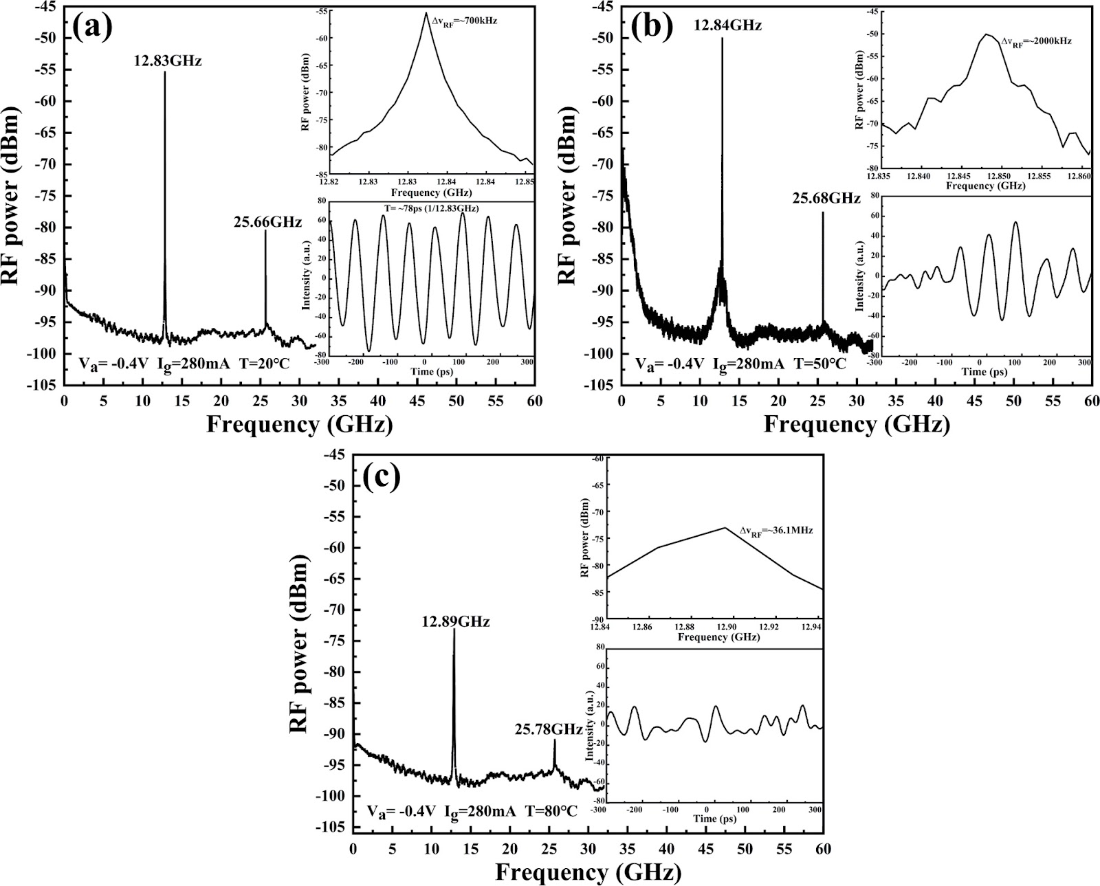
The optical soliton characteristics of GaSb-based ~2 μm wavelength integrated optical chips have broad application prospects in optoelectronic fields such as optical communications, infrared countermeasures, and gas environment monitoring. In the research of two-section integrated optical chips, more attention is paid to their passive mode-locked characteristics. The ability of its structure to generate stable soliton transmission has not yet been studied, which will limit its further application in high-performance near-mid infrared optoelectronic technology. In this paper, we design and prepare a GaSb-based ~2 μm wavelength two-section integrated semiconductor laser chip structure, and test and analyze its related properties of soliton, including power−injection current−voltage (P−I−V), temperature and mode-locked characteristics. Experimental results show that the chip can achieve stable mode-locked operation at nearly ~2 μm wavelength and present the working characteristics of near optical soliton states and multi-peak optical soliton states. By comparing and analyzing the measured optical pulse sequence curve with the numerical fitting based on the pure fourth order soliton approximation solution, it is confirmed that the two-section integrated optical chip structure can generate stable transmission of multi-peak optical soliton. This provides a research direction for developing near-mid infrared mode-locked integrated optical chips with high-performance property of optical soliton.

Research on optical soliton characteristics GaSb-based ~2 μm wavelength two-section integrated optical chip
Graphical Abstract
Original ResearchVol. 32, Issue 3 • pp. 100-112DOI: 10.1088/1674-4926/25030043Jan 15, 2025

Simulation and fabrication of vertical channel transistors with self-aligned high-κ metal gates using ion implantation for source/drain doping

Authors: Penghui Sun, Yongkui Zhang, Jun Luo

In vertical channel transistors (VCTs), source/drain ion implantation (I/I) represents a significant technical challenge due to inherent three-dimensional structural constraints, which induce complications such as difficulties in dummy gate formation and shadowing effects of I/I. This article systematically investigates the impact of different implantation conditions on the performance of VCTs with and without dummy gates through TCAD simulation. It reveals the significant role of the lightly doped regions (LDRs) naturally formed due to ion implantation in source/drain of VCTs. Furthermore, it was found that VCT without dummy gates can achieve an approximately 27% increase in on-state current (Ion) under the same implantation conditions, and can greatly simplify the process flow and reduce costs. Finally, N-type and P-type VCTs were successfully fabricated using this implantation method.

Simulation and fabrication of vertical channel transistors with self-aligned high-κ metal gates using ion implantation for source/drain doping
Graphical Abstract
Original ResearchVol. 32, Issue 3 • pp. 100-112DOI: 10.1088/1674-4926/25030030Jan 15, 2025

A high reliability NOR flash cell in 50 nm node technology

Authors: Kevin Fang, Wei Wang, Yibai Xue, Fan Wang, Dong Pan, Yi Li, Jerry Zhou

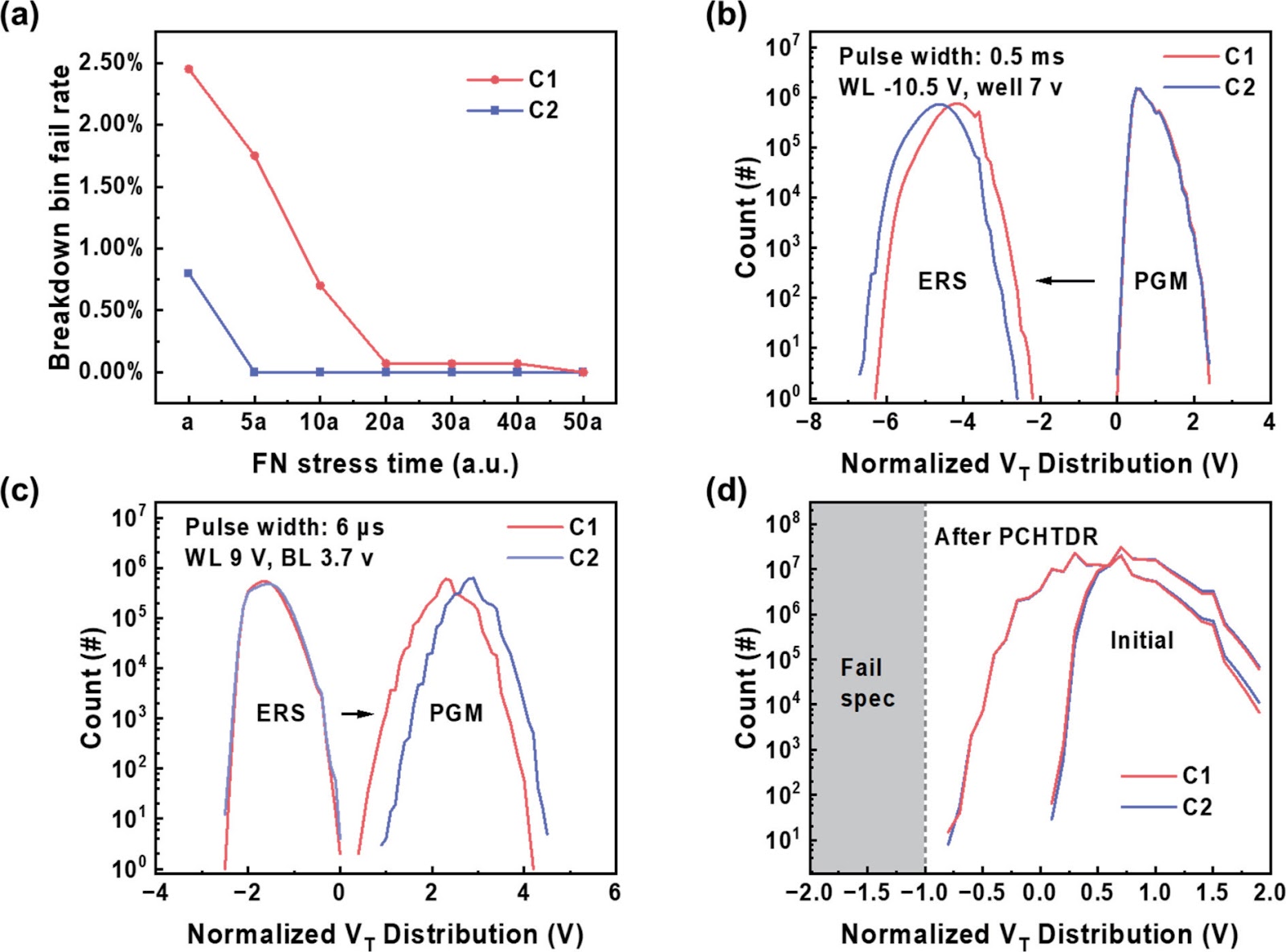
Along with NOR flash cell scaling down, dielectric burnout has gradually become one of the most important factors which affects product reliability, especially for high dropout voltage films. In this study, we demonstrate a reliability-enhanced NOR flash cell in 50 nm node technology through structural optimization of floating gate (FG) dimensions and active area profile. By synergistically increasing FG thickness, reducing FG width, and tuning cell-open depth, the control gate-to-active area corner distance expands by 22%, suppressing peak electric fields by 29% vertically and 18% horizontally. This structural innovation achieves: (1) 100× reduction in early-cycle burnout failures, (2) 7.38× time dependent dielectric breakdown lifetime improvement, while maintaining data retention and accelerating programming/erasing speeds by 15.4%/7.3%. The enhanced reliability enables 97.5% reduction in Fowler−Nordheim stress time during characterization program testing, providing a cost-effective solution for automotive-grade flash memories.

A high reliability NOR flash cell in 50 nm node technology
Graphical Abstract
Original ResearchVol. 32, Issue 3 • pp. 100-112DOI: 10.1088/1674-4926/25030017Jan 15, 2025

High-responsivity and high-speed germanium photodetector for C + L application

Authors: HU Yiling, LIU Zhipeng, LIU Zhi, ZHU Yupeng, MEN Tao, ZHANG Guangze, ZHENG Jun, ZUO Yuhua, CHENG Buwen

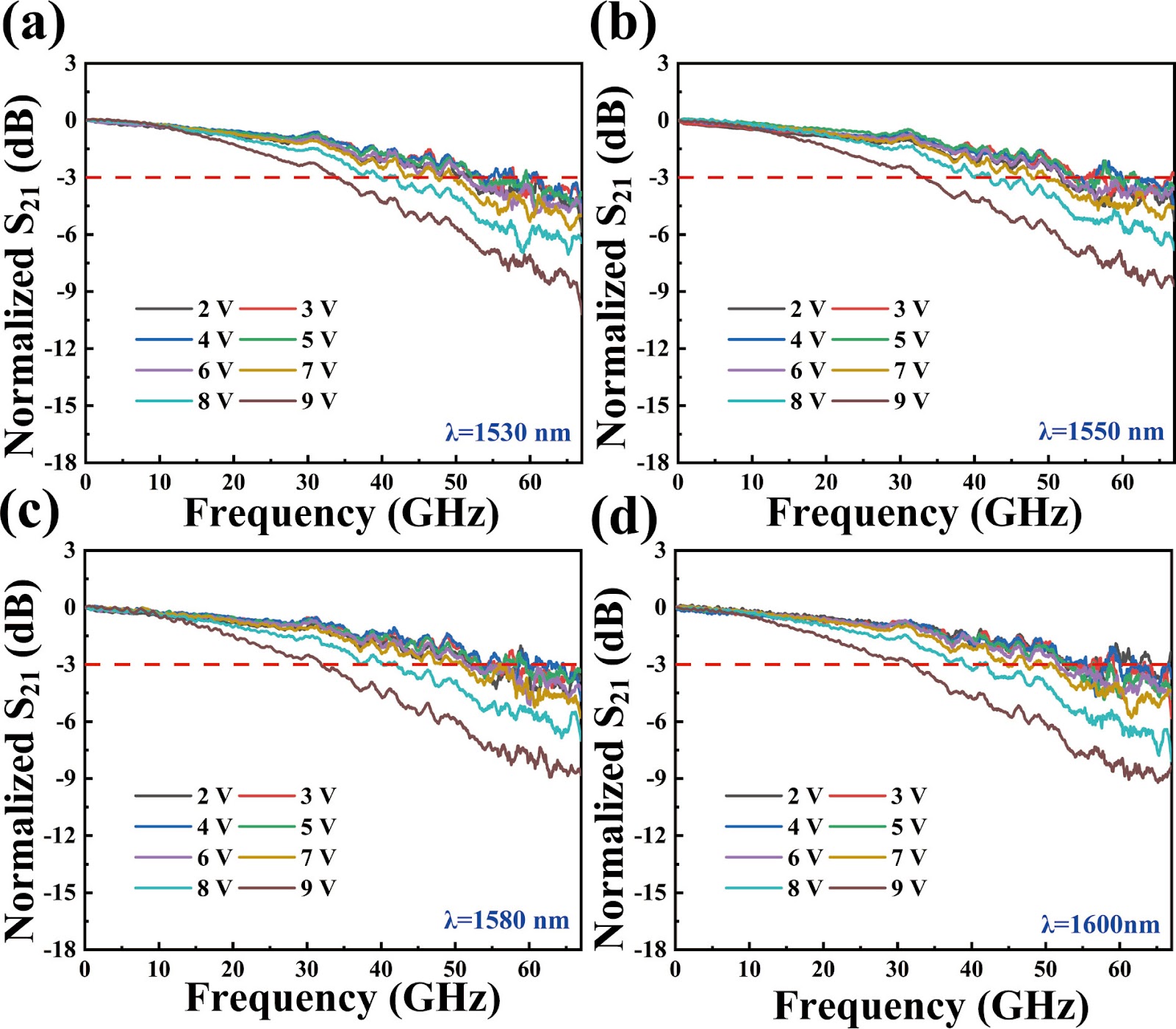
A silicon-based germanium (Ge) photodetector working for C and L bands is proposed in this paper. The device features a novel asymmetric PIN structure, which contributes to a more optimized electric field distribution in Ge and a shorter effective width of depleted region. Meanwhile, the optical structure is designed carefully to enhance responsivity for broadband. Under −7 V, where the weak avalanche process happens, the responsivity of our device is 1.49 and 1.16 A/W at 1550 and 1600 nm, with bandwidth of 47.1 and 44.5 GHz, respectively. These performances demonstrate the significant application potential of the device in optical communication systems.

High-responsivity and high-speed germanium photodetector for C + L application
Graphical Abstract
Original ResearchVol. 32, Issue 3 • pp. 100-112DOI: 10.1088/1674-4926/25030039Jan 15, 2025

Influencing factors of noise characteristics in EBCMOS with uniformly doped P-type substrates

Authors: Xinyue He, Gangcheng Jiao, Hongchang Cheng, Tianjiao Lu, Ye Li, De Song, Weijun Chen

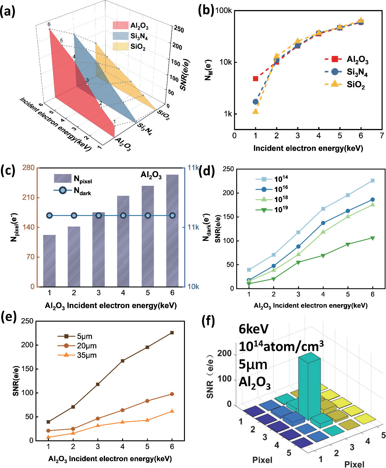
In this study, with the aim of achieving a high signal-to-noise ratio (SNR) in an electron-bombarded complementary metal−oxide−semiconductor (EBCMOS) imaging chip, we analyzed the sources of noise using principles from low-light-level imaging and semiconductor theory, and established a physical computational model that relates the electron-multiplication layer to the noise characteristics of an EBCMOS chip in a uniformly doped structure with a P-type substrate. We conducted theoretical calculations to analyze the effects on noise characteristics of the passivation layer material and thickness, P-substrate doping concentration, P-substrate thickness, incident electron energy, and substrate temperature. By comparing the characteristics of pixel noise, dark current, multiplication electron numbers, and SNR under various structures, we simulated optimized structural parameters of the device. Our simulation results showed that the noise characteristics of the device could be optimized using an Al2O3 passivation thickness of 15 nm and substrate temperature of 260 K, and by decreasing the doping concentration and thickness of the P-type substrate and increasing the incident electron energy. The optimized SNR were 252 e/e. And the substantial impact of dark current noise, primarily governed by interfacial defects, on the overall noise characteristics of the device. This research offers theoretical support to develop EBCMOS imaging chips with high gain and SNR.

Influencing factors of noise characteristics in EBCMOS with uniformly doped P-type substrates
Graphical Abstract