SinoTechIntel Academic Portal
🏛️ Indexed Academic JournalImpact Factor: 3.8

Opto-Electronic Advances (光电进展)

Authoritative peer-reviewed journal in materials science, metallurgy, chemistry and engineering technologies: Opto-Electronic Advances (光电进展)

Total Research Papers: 148
Access: 100% Free Open Access
Browse by Publication Year & VolumeReset All Filters ✕

Published Research PapersFiltered: Year 2026 • Vol. 32

Showing 24 of 148 peer-reviewed papers with full Graphical Abstracts.

Original ResearchVol. 32, Issue 1 • pp. 100-112DOI: 10.29026/oea.2026.250249Jan 15, 2026

Polarization-guided diffusion prior for eyeglass reflection removal

Authors: Yating CHEN, Liangcai CAO

Eyeglass reflection severely degrades facial feature visibility in video conferencing and facial recognition, where the captured image is a superposition of transmission and reflection layers. Existing polarization-based reflection removal methods depend on large-scale paired polarization datasets, limiting generalization to unseen lighting conditions. This work introduces PDPrior, an untrained polarization-guided diffusion prior that requires no training data and no ground-truth reflection-free images. PDPrior leverages the generative prior of a diffusion model and incorporates polarization information as guidance to control the generation process. The reflection diffusion model uses the degree of linear polarization (DoLP) to preliminarily identify reflection regions and exploits the diffusion prior of progressively darkening facial content, enabling focus on reflective areas. The transmission coefficient computed from DoLP guides transmission image generation via the physical forward model of reflection formation. During each sampling step, reflection and transmission variables are alternately updated through gradient descent based solely on the test sample, conferring adaptability to complex lighting and diverse scenes. Real-world eyeglass reflection images were collected using a division-of-focal-plane polarization camera under various indoor and outdoor lighting environments. Experimental results demonstrate that PDPrior effectively removes eyeglass reflection, producing high-fidelity face reconstructions with no visible artifacts and achieving more robust face image quality assessment scores for recognition performance. The framework generalizes to window photography, showcase displays, and driver monitoring.

Polarization-guided diffusion prior for eyeglass reflection removal
Graphical Abstract
Original ResearchVol. 32, Issue 1 • pp. 100-112DOI: 10.29026/oea.2026.250197Jan 15, 2026

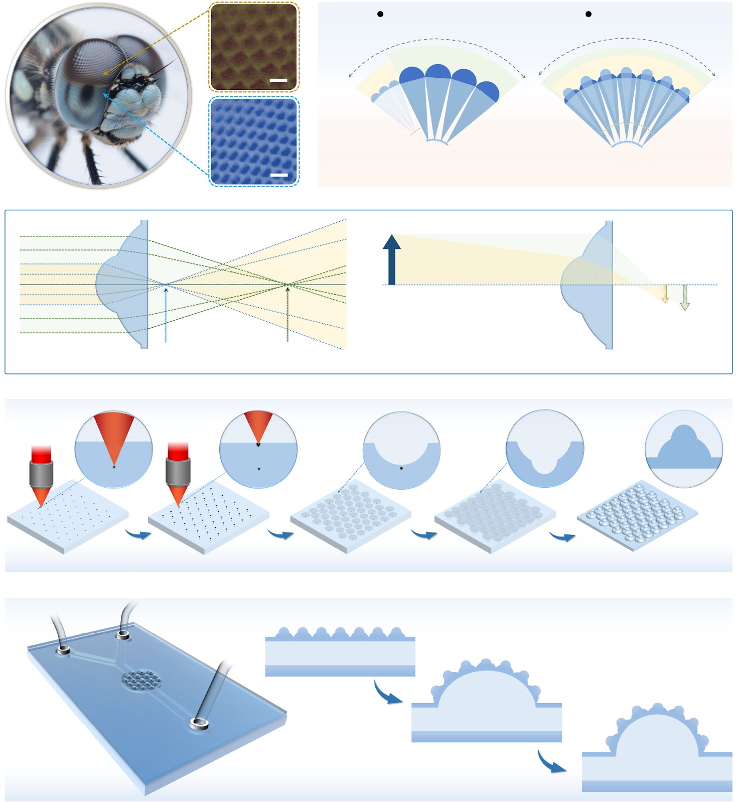
Tunable Compound Eyes with Coaxial Lens-on-Lens Ommatidia for Cooperative Bi-Focal Imaging

Authors: SUN Zhi-Juan, ZHONG Wei-Jian, CAI Qing, LU Yi-Fan, LI Chang-Xu, HAN Dong-Dong, ZHANG Yong-Lai

Artificial compound eyes (CEs) remain inferior to insect counterparts in ommatidial spatial arrangement, size distribution, visual field adaptability, and environmental perception. This work presents a tunable bionic CE with coaxial lens-on-lens (LoL) ommatidia, inspired by Sympetrum frequens, integrating a flexible polydimethylsiloxane (PDMS) LoL array with a microfluidic chip to achieve simultaneous bi-focal imaging. The LoL array was fabricated via femtosecond laser dual-modification of quartz glass, two-step wet etching, and soft lithography, yielding a concave template of approximately 2.6 mm². Integration with a microfluidic chamber enabled liquid-pressure modulation of CE configurations, producing a complete curved bi-focal plane that overcomes the limitations of single-focal-plane and regionalized nonuniform ommatidia CEs. Optical characterization confirmed stable focusing performance for both large and small ommatidia within their theoretical fields of view (FOVs). Cooperative bi-focal imaging was achieved by regulating FOV and relative positions of different LoL ommatidia through controlled injection of PDMS precursor. Large-FOV imaging and moving target monitoring were demonstrated, with reconstructed trajectories of triangular and dragonfly targets in 3D coordinates. The tunable CE with LoL ommatidia offers significant potential for particle image velocimetry, robotic vision, and virtual endoscopy, providing a scalable route to advanced micro-optical systems with adaptive visual field and depth perception.

Tunable Compound Eyes with Coaxial Lens-on-Lens Ommatidia for Cooperative Bi-Focal Imaging
Graphical Abstract
Original ResearchVol. 32, Issue 1 • pp. 100-112DOI: 10.29026/oea.2026.250263Jan 15, 2026

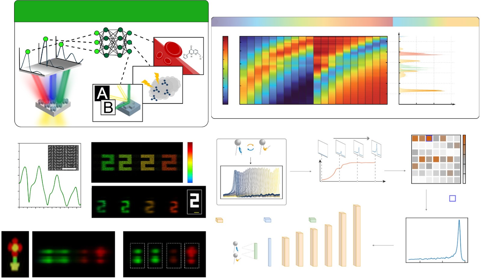
AI-assisted metaphotonics: A Comprehensive Review of Artificial Intelligence-Driven Approaches for Metaphotonic Systems

Authors: Minsung Kang, Seokju Choi, Kaixi Fu, Xiaoyuan Liu, Zhun Wei, Lei Jin, Hao Wang, Olivier J. F. Martin, Joel K. W. Yang, Sunae So, Trevon Badloe

The convergence of artificial intelligence (AI) and metaphotonics is creating a new paradigm for controlling light-matter interactions. The synergy of AI's ability to learn complex relationships in multidimensional data and provide ultra-fast inference with the capacity of metaphotonics to engineer optical properties not found in nature is unlocking a new era in computational design, real-time control, and fully automated optical systems. This review provides a comprehensive overview of state-of-the-art AI-driven approaches for metaphotonic systems. We focus on the solutions to real-world problems in accelerating metaphotonic simulations and inverse design, optical data characterization, and the development of fully integrated end-to-end AI-assisted metaphotonic systems. Finally, we provide our perspectives on the future research directions and emerging opportunities at the rapidly evolving intersection of metaphotonics and AI.

AI-assisted metaphotonics: A Comprehensive Review of Artificial Intelligence-Driven Approaches for Metaphotonic Systems
Graphical Abstract
Original ResearchVol. 32, Issue 1 • pp. 100-112DOI: 10.29026/oea.2026.260058Jan 15, 2026

Polarization Unlocks Scene-Level 3D Imaging: A Commentary on Integration-Free Binocular-Polarization Fusion for Discontinuous Targets

Authors: David Brady

Scene-level high-precision 3D imaging remains constrained by the fundamental trade-off between imaging distance and depth accuracy. Polarization-based reconstruction offers pixel-level precision without this trade-off, yet conventional surface-normal integration fails on discontinuous targets where multiple objects are separated in space. Liu et al. (Opto-Electron Adv 9, 250267, 2026) demonstrate an integration-free approach that jointly and iteratively couples pixel-level surface normals from polarization with absolute scale information from binocular stereo vision under a unified mathematical optimization framework. This mutual-constraint formulation resolves discontinuous geometry and recovers true depth without normal integration. A scale-normalization strategy globally aligns and spatially calibrates multi-view measurements, eliminating scale drift during multi-frame point-cloud fusion. Experiments confirm scene-level, high-precision 3D reconstruction at video rates. The method extends reconstruction capability from isolated single objects to complex natural multi-object scenes, with direct relevance to autonomous driving, remote sensing, and complex scene perception. Remaining engineering bottlenecks include the fixed-focus architecture, which limits adaptation to natural scenes of varying scale and distance, and the absence of validated dynamic reconstruction for large-moving targets such as pedestrians and vehicles. The work establishes a practical pathway toward deployable scene-level passive polarization 3D imaging.

Polarization Unlocks Scene-Level 3D Imaging: A Commentary on Integration-Free Binocular-Polarization Fusion for Discontinuous Targets
Graphical Abstract
Original ResearchVol. 32, Issue 1 • pp. 100-112DOI: 10.29026/oea.2026.250260Jan 15, 2026

Optoelectronic Advances in the Hybrid Plasmonic Metasurface for Multi-Band and Wide-Spectrum Photodetection

Authors: ZHANG Wei, LI Ming, WANG Fang, LIU Yang, CHEN Hao

Hybrid plasmonic metasurfaces have emerged as a pivotal platform for enhancing photodetection across multiple bands, yet their practical deployment is constrained by narrow operational bandwidth and high dark current. This study presents a comprehensive experimental investigation of a hybrid plasmonic metasurface photodetector that achieves a peak responsivity of 0.45 A/W at 1550 nm and a specific detectivity of 1.2 × 10^11 Jones, with a dark current density of 2.5 nA/cm² at room temperature. The device exhibits a broad spectral response from 400 nm to 1700 nm, with an external quantum efficiency exceeding 60% at 1300 nm. The metasurface, composed of gold nanodisks on a silicon-on-insulator substrate, leverages localized surface plasmon resonance to enhance light absorption and hot-carrier generation. Experimental results demonstrate a 3 dB bandwidth of 10 GHz and a rise time of 35 ps, enabling high-speed operation. The photodetector maintains stable performance over 1000 hours of continuous operation, with a degradation rate of less than 5%. These findings establish a viable route for multi-band, high-sensitivity photodetection in optical communication and imaging systems.

Original ResearchVol. 32, Issue 1 • pp. 100-112DOI: 10.29026/oea.2026.250216Jan 15, 2026

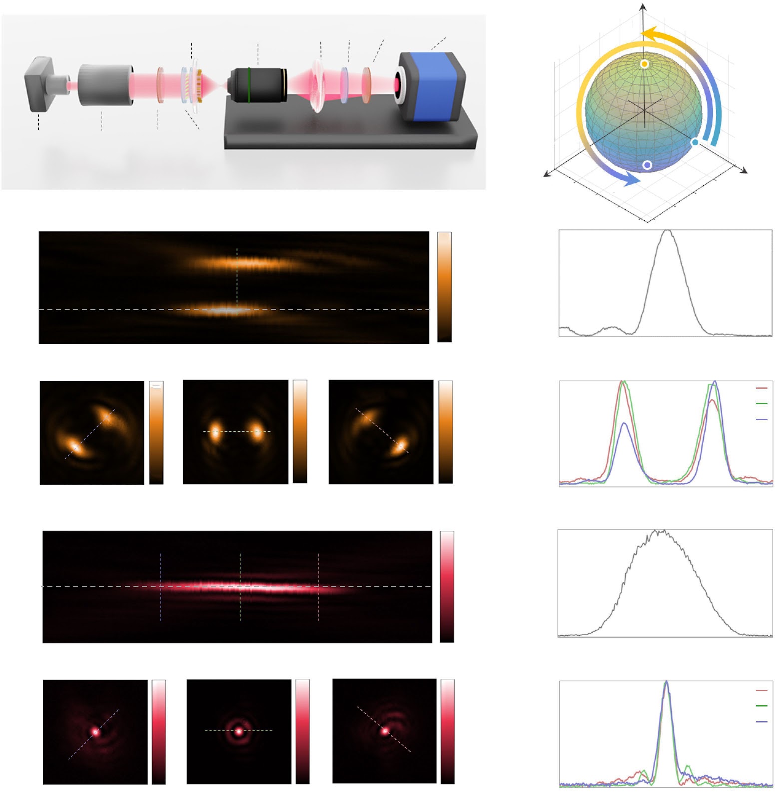
Millisecond-level electrically switchable metalens for adaptive rotational depth mapping and diffraction-limited imaging

Authors: Yeseul Kim, Jihae Lee, Won-Sik Kim, Hyeonsu Heo, Dongmin Jeon, Beomha Yang, Xiaotong Li, Harit Keawmuang, Shiqi Hu, Young-Ki Kim, Trevon Badloe, Junsuk Rho

The intrinsic trade-off between depth-of-focus and lateral resolution in conventional optical systems constrains three-dimensional imaging in compact form factors. This work demonstrates an electrically tunable dual-mode metalens that integrates hydrogenated amorphous silicon (a-Si:H) meta-atoms with a liquid crystal (LC) modulator to independently manipulate left- and right-circularly polarized (LCP/RCP) light at 635 nm. Under LCP illumination, the metalens generates a rotating double-helix point spread function (PSF) encoding depth via rotation angle; under RCP illumination, it produces an extended depth-of-focus with a narrow PSF for high-resolution imaging. Propagation and geometric phases were co-optimized via rigorous coupled-wave analysis (RCWA), yielding high transmittance and precise phase control. Experimental characterization confirmed near-diffraction-limited lateral and axial resolutions. The integrated LC cell enables millisecond-scale polarization switching between depth-sensitive and high-resolution modes. Depth extraction was validated by correlating rotation angles of dual-image focal spots under mixed-polarization illumination, with axial displacements of Δz1 = 30.5 μm, Δz2 = 0 μm, and Δz3 = −48.3 μm corresponding to rotation angles β = −25.6°, 0°, and 16.9°, respectively. Depth-resolved imaging of a rubber-tree leaf, skeletal-muscle cross-section, and live planarian retrieved color-coded depth maps, demonstrating efficacy on complex biological tissues. This polarization-driven platform offers a compact solution for biomedical imaging, three-dimensional sensing, and adaptive optics.

Millisecond-level electrically switchable metalens for adaptive rotational depth mapping and diffraction-limited imaging
Graphical Abstract
Original ResearchVol. 32, Issue 1 • pp. 100-112DOI: 10.29026/oea.2026.250270Jan 15, 2026

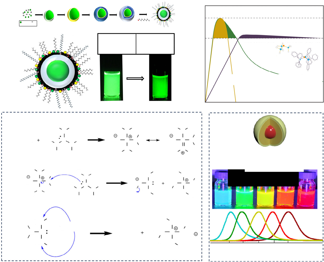
Overcoming Challenges in InP-Based Quantum Dots: From Nucleation Mechanisms to High-Performance Quantum Dot Light-Emitting Diodes

Authors: BIAN Yangyang, LI Qian, CHEN Fei, YANG Chunhe, SHEN Huaibin, TANG Aiwei

Indium phosphide-based quantum dots (InP QDs) are positioned as the leading cadmium-free alternative for next-generation display and optoelectronic technologies, offering high photoluminescence quantum yield (PL QY), narrow emission spectra, and size-tunable wavelengths. Commercial deployment, however, remains constrained by synthetic and processing bottlenecks. State-of-the-art InP QD systems typically deliver PL QY below 90% and emission linewidths exceeding 35 nm, while device external quantum efficiency (EQE) and operational lifetime improve only incrementally. This review systematically examines the nucleation mechanisms governing InP core formation and evaluates optimization strategies for core/shell heterostructures, ligand engineering, and device architecture. A comprehensive analysis of recent breakthroughs in red, green, and blue InP-based quantum dot light-emitting diodes (QLEDs) is presented, with emphasis on charge transport modulation and suppression of charge leakage. Despite progress, a significant performance gap persists for practical display applications. Critical unresolved challenges include achieving high-performance electroluminescence from small QDs, mitigating imbalanced carrier injection that drives Auger recombination, Joule heating, and low recombination efficiency, elucidating luminescence and aging mechanisms, and improving blue-emitting device performance. The review concludes by outlining pathways to overcome these limitations, including fabrication of large-sized InP QDs with near-unity PL QY, enhancement of radiative recombination and light extraction efficiency, advanced characterization of degradation mechanisms, and performance enhancement of blue InP-based QLEDs.

Overcoming Challenges in InP-Based Quantum Dots: From Nucleation Mechanisms to High-Performance Quantum Dot Light-Emitting Diodes
Graphical Abstract
Original ResearchVol. 32, Issue 1 • pp. 100-112DOI: 10.29026/oea.2026.250224Jan 15, 2026

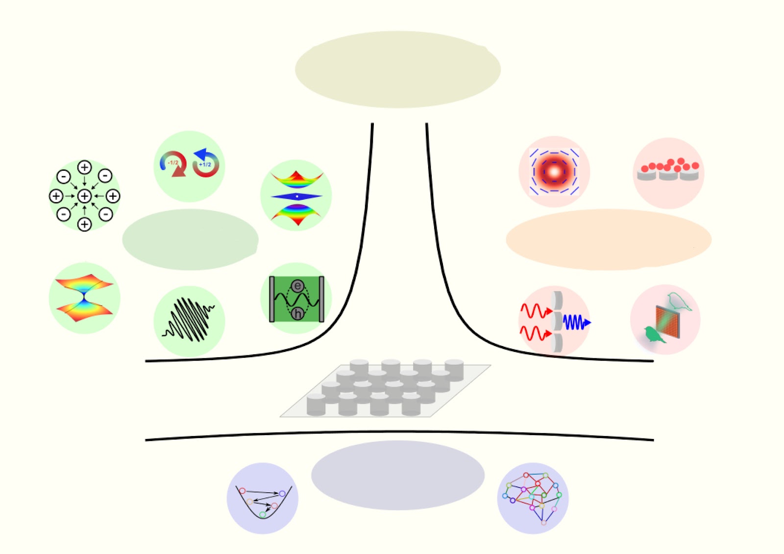
Emerging landscape of photonic bound states in the continuum for next-generation metadevices

Authors: DO Thi Thu Ha, LIN Ronghui, SHILKIN Daniil A., YUAN Zhiyi, DANG Cuong, KUZNETSOV Arseniy I., TENG Jinghua, HA Son Tung

Bound states in the continuum (BICs) have emerged as a central paradigm in nanophotonics, offering theoretically unbounded quality factors (Q) and topologically protected mode confinement within the radiative continuum. This review critically examines the trajectory of BIC research from foundational predictions by Wigner and von Neumann (1929) and semiconductor superlattice observations by Capasso et al. (1992) to contemporary metasurface implementations. We analyze design methodologies including machine learning and inverse design, and survey emergent BIC classes: super-BICs, chiral BICs, flatband BICs, and Moiré BICs. The integration of phase-change materials and liquid crystals enables dynamic control over emission and absorption, while strong light-matter interaction, ultrafast dynamics, and exceptional points are assessed for device relevance. Key application domains—lasing, optical sensing, and nonlinear optics—are evaluated with emphasis on conversion efficiency and sensitivity thresholds. We identify persistent challenges in fabrication tolerance, material loss, and scalable integration. The review concludes with perspectives on multilayer metasurfaces, quantum emitter interfacing, and pathways toward commercial BIC metadevices, providing a rigorous framework for researchers and engineers targeting high-performance photonic systems.

Emerging landscape of photonic bound states in the continuum for next-generation metadevices
Graphical Abstract
Original ResearchVol. 32, Issue 1 • pp. 100-112DOI: 10.29026/oea.2026.250177Jan 15, 2026

Soft Chiral Superstructure Enabled Dynamic Polychromatic Holography

Authors: XU Chun-Ting, LI Lu, CHEN Quan-Ming, WANG Guang-Yao, HU Wei

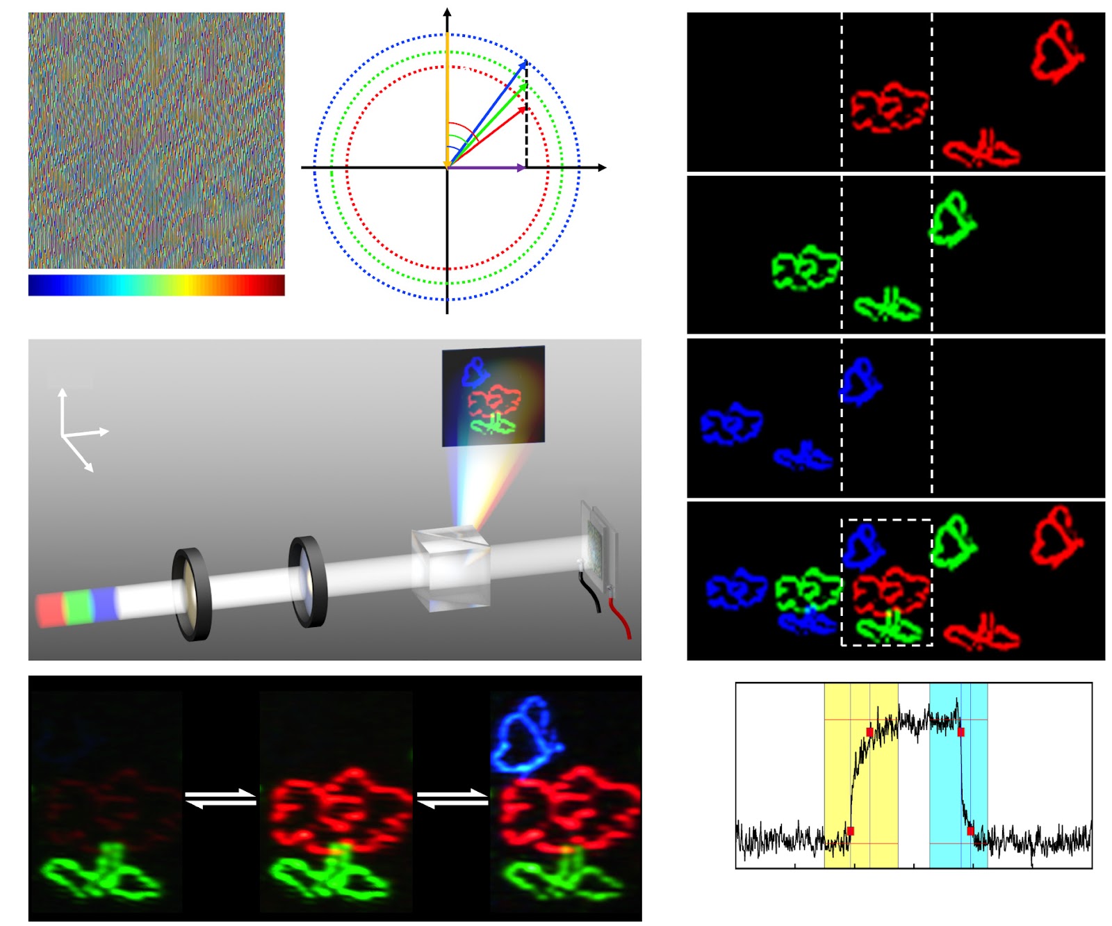
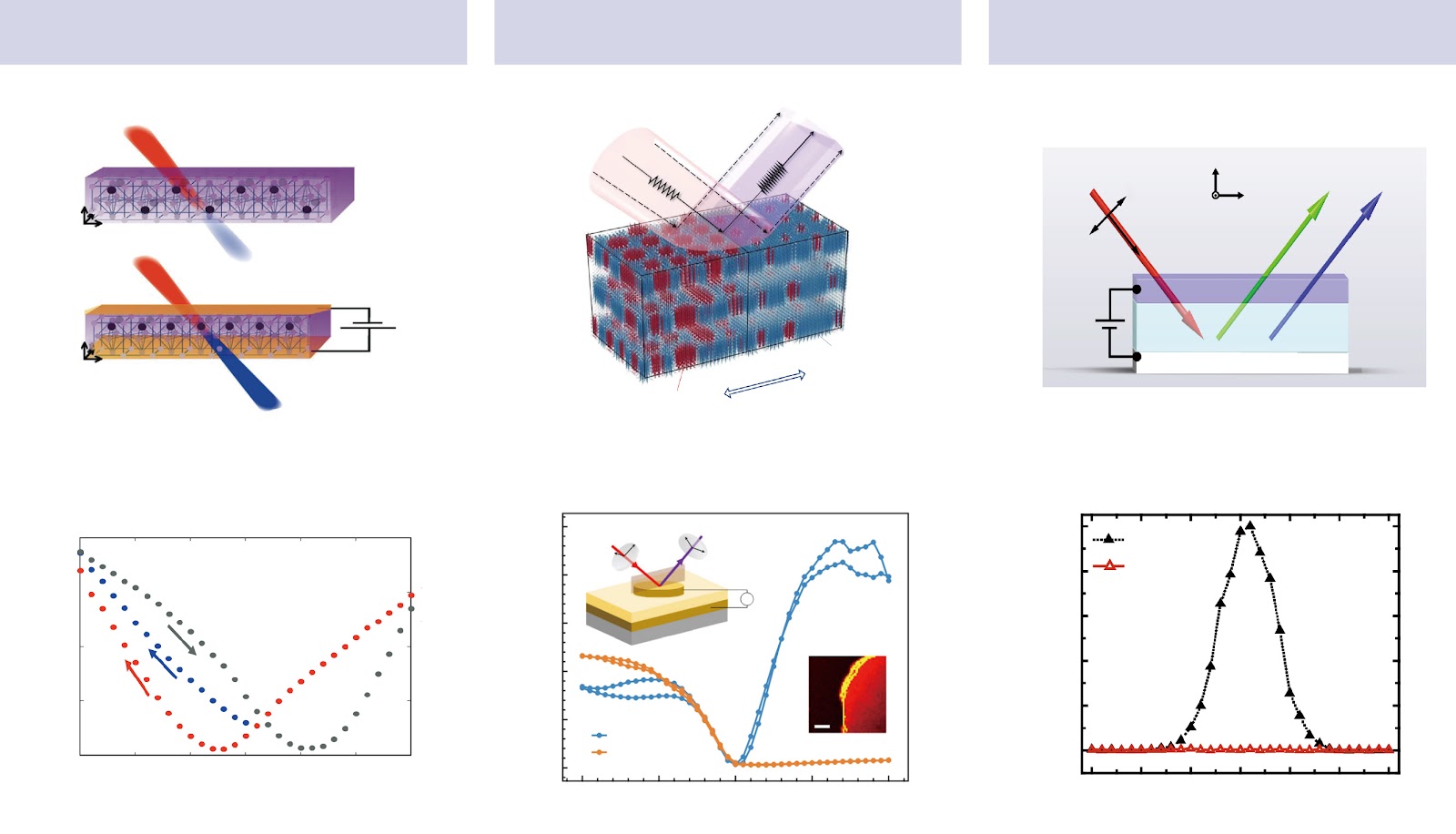
Planar optics offers a compact and versatile platform for manipulating multiple dimensions of light parameters and thus has attracted tremendous interest in high-density data storage, high-security information encryption, and holographic displays. It is still challenging to achieve active functionalities via dynamically operating light-matter interactions inside these planar optics. Here, a polymer-stabilized cholesteric liquid crystal (CLC) is adopted as a tunable one-dimensional chiral superstructure. The bandgap tends to change from a periodic helix to a gradient-pitch configuration under direct current (DC) voltage, and the reflection bandwidth varies from a narrow band of 40 nm to a broad band of 180 nm. Off-axis phase-only holograms of three primary colors are properly k-space engineered via a modified Gerchberg-Saxton algorithm, and recorded into the initial alignments of the CLC by photopatterning. By altering the applied DC voltage, the generated holography actively switches between a monochromatic and polychromatic image. Moreover, spin-selective Bragg-Berry phase encoding in photopatterned superstructures with opposite helicity allows distinct holograms (e.g., "weather sign" and "chameleon") to be independently generated and modulated. This work takes full advantage of soft chiral superstructures for on-demand light control and has great potential in dynamic holography, information encryption, and data storage.

Soft Chiral Superstructure Enabled Dynamic Polychromatic Holography
Graphical Abstract
Original ResearchVol. 32, Issue 1 • pp. 100-112DOI: 10.29026/oea.2026.250238Jan 15, 2026

Perovskite Nanocrystals in Glass for High Efficiency and Ultra-High Resolution Dynamic Holographic Multicolor Display

Authors: Chao Ruan, Xinkuo Li, Ke Sun, Jianrong Qiu, Dezhi Tan

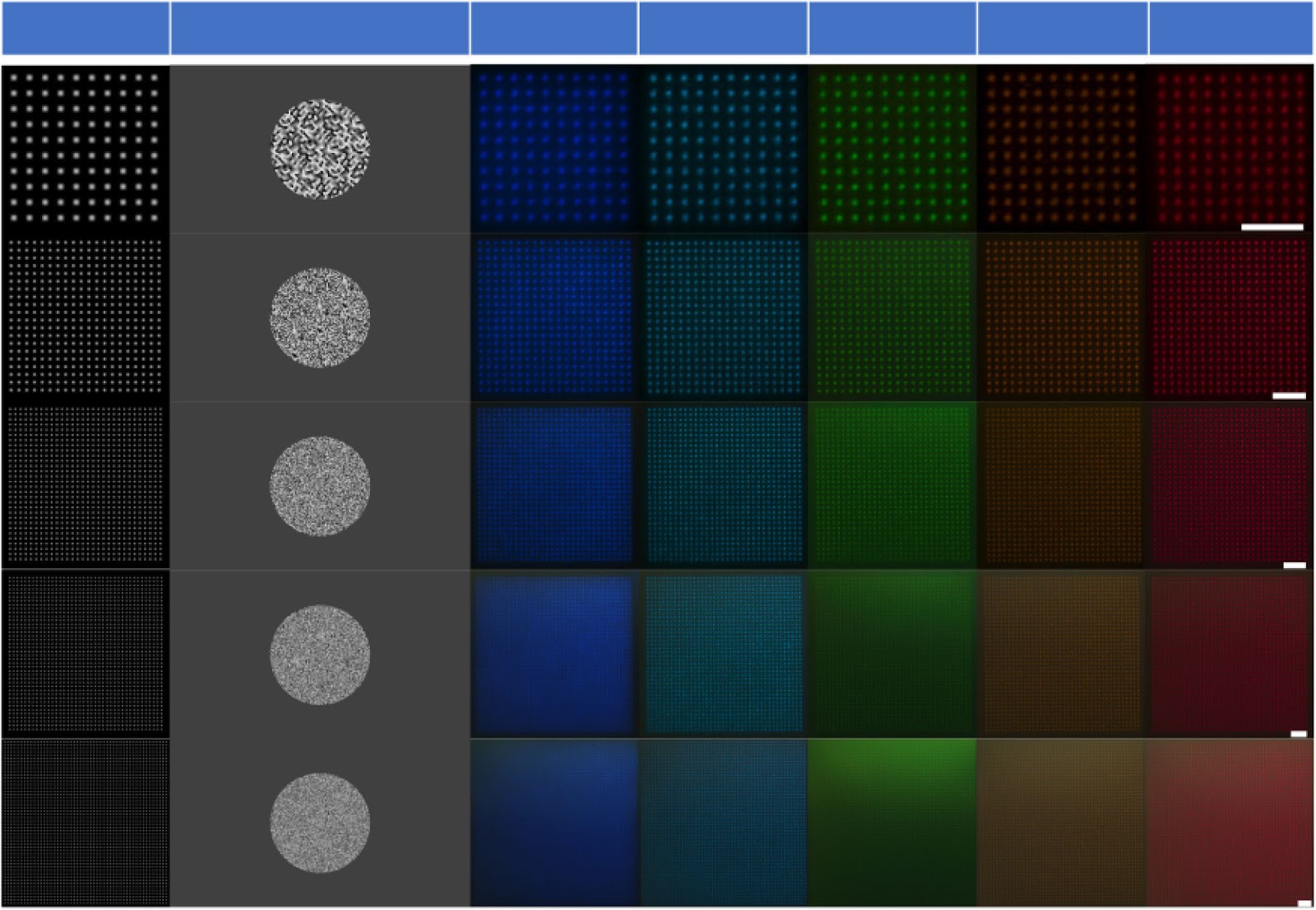
Embedding CsPbX3 (X=Cl, Br, I) perovskite nanocrystals (PNCs) within inorganic glass matrices mitigates their intrinsic environmental instability, yet simultaneous attainment of high luminance and high photoluminescence quantum yield (PLQY) remains impeded by strong self-absorption. This study introduces fluoride ion doping to modify the three-dimensional glass network, thereby optimizing PNC crystallization behavior and enabling full-spectrum high luminance and high PLQY. The optimized PNCs-glass composites achieve a record PLQY of 36% for pure blue emission (<480 nm) while maintaining high luminance. The robust glass matrix provides excellent encapsulation, ensuring stability against ambient light, heat, and chemical solvents. Integrating these composites with a spatial light modulator (SLM) and computer-generated holograms (CGHs) yields a dynamic holographic multicolor display with pixel density up to 20,247 pixels per inch (PPI). A vertically stacked multilayer full-color architecture is further demonstrated, surpassing conventional planar color display technologies in resolution and light utilization efficiency. The CIE 1931 color gamut covers 112.7% of the NTSC standard. This work establishes a promising paradigm for energy-efficient, ultra-high-resolution displays.

Perovskite Nanocrystals in Glass for High Efficiency and Ultra-High Resolution Dynamic Holographic Multicolor Display
Graphical Abstract
Original ResearchVol. 32, Issue 1 • pp. 100-112DOI: 10.29026/oea.2026.260073Jan 15, 2026

Remote-Mode Microsphere-Enabled Nanoscale Imaging Technology for Real-Time, Label-Free Semiconductor Inspection: From Laboratory Innovation to Commercial Deployment

Authors: Zheting Meng, Lianwei Chen, Mingbo Pu, Xiangang Luo, Minghui Hong

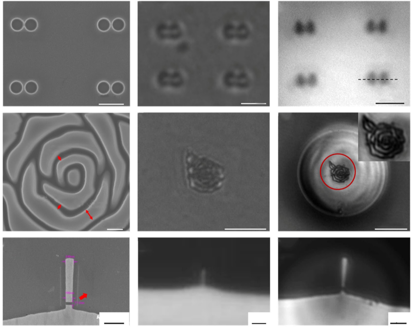
Conventional optical microscopy is fundamentally constrained by the optical diffraction limit of approximately 200 nm, which restricts the observation of critical nanoscale features in advanced manufacturing, semiconductor defect inspection, and biomedical research. This study presents a remote-mode microsphere-enabled nanoscale imaging technology that overcomes this limitation through the use of a suspended transparent microsphere functioning as a miniature lens. The system forms a magnified virtual image via light refraction at the microsphere surfaces, which is captured by a standard objective lens and reconstructed through reverse optical-path analysis. Experimental validation demonstrates that a 20 μm silica microsphere integrated with a 100× oil-immersion objective (NA = 1.4) resolves 23 nm gaps on silicon wafers and 77 nm metal probe gaps in hard-disk magnetic heads, achieving performance comparable to scanning electron microscopy. A universal lens adapter incorporating a 400 μm microsphere enables a standard 20× objective to attain imaging performance equivalent to a 50× objective at one-tenth the cost of high-end super-resolution systems. The technology has been commercialized by PHAOS Technology, achieving over 300% annual sales growth and receiving the Manufacturing Technology Disruptor of the Year award. This approach provides a scalable, cost-effective solution for real-time, non-contact, label-free nanometrology in semiconductor inspection and industrial quality control.

Remote-Mode Microsphere-Enabled Nanoscale Imaging Technology for Real-Time, Label-Free Semiconductor Inspection: From Laboratory Innovation to Commercial Deployment
Graphical Abstract
Original ResearchVol. 32, Issue 1 • pp. 100-112DOI: 10.29026/oea.2026.250211Jan 15, 2026

Pixelated BIC Metasurfaces for Terahertz Integrated Sensing and Imaging

Authors: XUE Zhanqiang, XU Guizhen, CHEN Junliang, FAN Junxing, XING Hongyang, ZHOU Ye, CONG Longqing

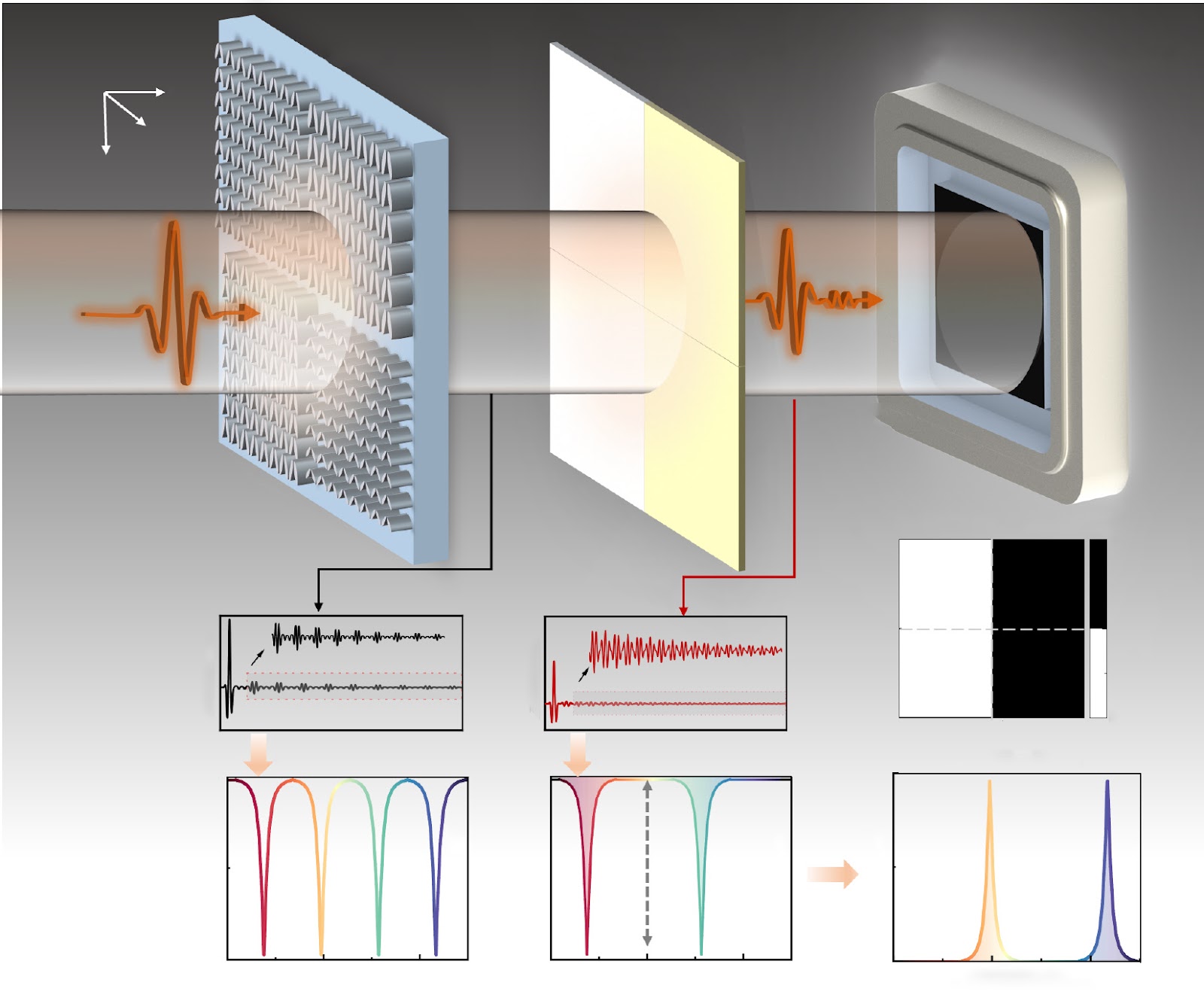
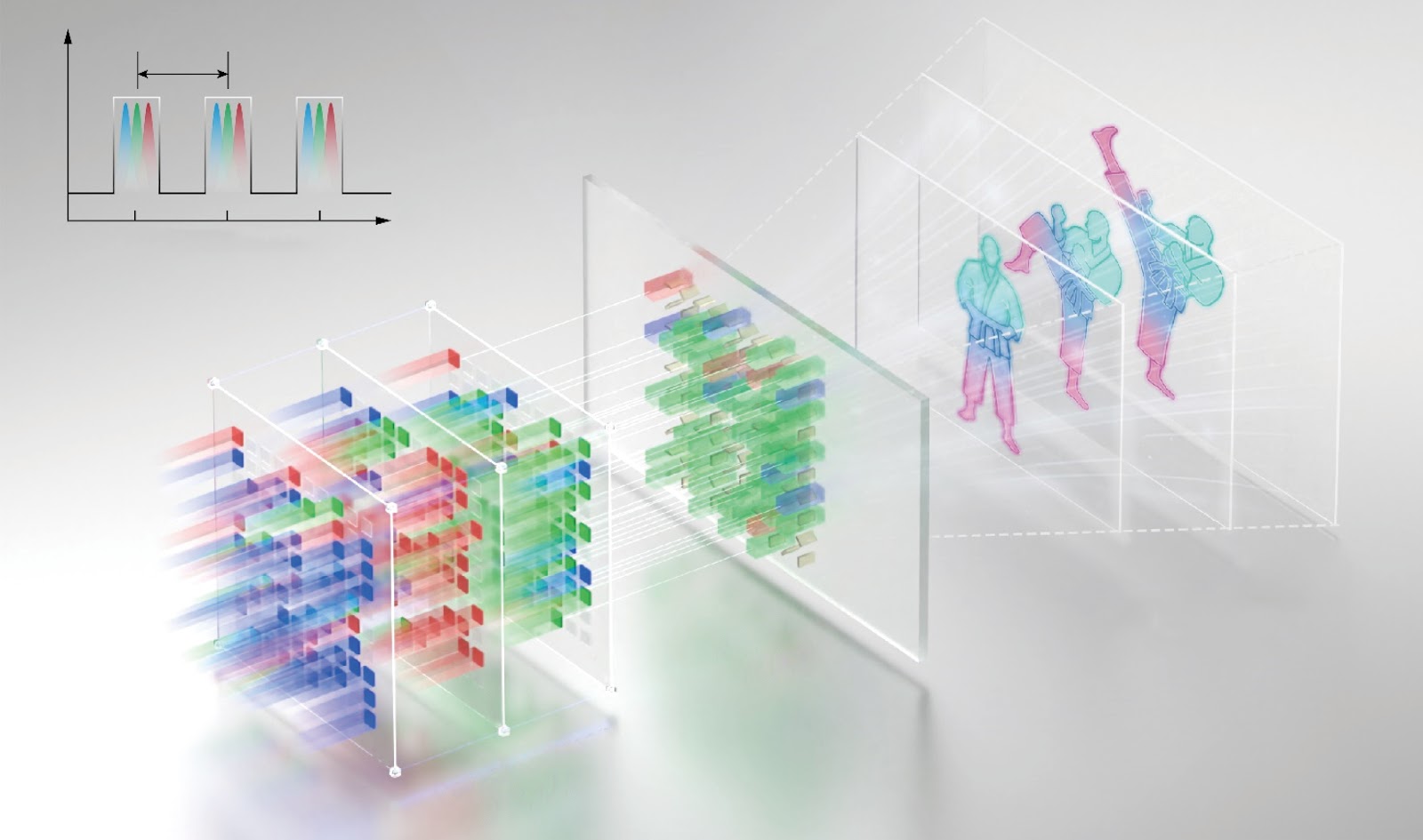
Conventional terahertz (THz) single-pixel imaging relies on sequential compressed sensing with spatial modulators, imposing severe acquisition latency and hardware complexity. This work demonstrates a parallelized THz single-pixel imaging scheme using a pixelated metasurface within a standard THz time-domain spectroscopy system. Spatial information is encoded through multiple narrow linewidth resonances rooted in bound states in the continuum (BIC) physics, while the BIC-enabled pixelated metasurface facilitates near-field distributed sensing via local field enhancement. A 2×2 metasurface array validates integrated imaging and sensing in a proof-of-concept experiment, with demonstrated scalability to larger arrays. The approach achieves 100% accuracy in binary imaging reconstruction from a single THz pulse and enables refractive index sensing with a sensitivity exceeding 14.39 GHz/RIU. Leveraging the intrinsic penetration capability of THz radiation, this technique offers significant promise for next-generation noninvasive applications such as security inspection and defect detection in semiconductor chips and pharmaceutical products.

Pixelated BIC Metasurfaces for Terahertz Integrated Sensing and Imaging
Graphical Abstract
Original ResearchVol. 32, Issue 1 • pp. 100-112DOI: 10.29026/oea.2026.260049Jan 15, 2026

Optical addressing enables a new architecture for spatial light modulators

Authors: HUANG Xiangyu, LIU Na

Spatial light modulators (SLMs) are indispensable in three-dimensional holographic displays, additive manufacturing, quantum optics, and adaptive imaging. The critical performance metric is spatiotemporal product density (STPD), defined as the number of independently addressable pixels per unit area multiplied by the modulation rate. Practical real-time 3D holography demands an STPD on the order of 10^12 pixels/(s·cm^2), a benchmark far beyond existing commercial and research SLM technologies. Liquid crystal on silicon (LCoS) and digital micromirror devices (DMD) have advanced steadily but remain constrained by pixel sizes of several micrometers—much larger than visible wavelengths. In LCoS, liquid crystal layer thickness and fringing-field effects limit pixel scalability without crosstalk or degraded phase modulation. In DMDs, mechanical constraints such as hinge stiffness restrict mirror miniaturization and switching speed. Achieving true wavelength-scale pixilated modulation in the visible range remains a formidable challenge, motivating exploration beyond conventional electro-optic and microelectromechanical systems. Metasurfaces have emerged as a versatile platform for subwavelength wavefront engineering, and their integration with commercial SLMs has improved spot-count scaling, dimensional conversion, and field-of-view expansion. Active metadevices based on phase-change materials and electrochemical actuation offer dynamic tuning but are typically limited to single-parameter modulation and millisecond-scale responses. Electrically addressed schemes, including liquid crystal-integrated metasurfaces and indium tin oxide (ITO)-based devices, present promising alternatives for pixel miniaturization, yet most implementations support only one-dimensional beam steering and still rely on micrometer-scale addressing. A recent work reports an optically addressed metasurface spatial light modulator (OA-MSLM) that achieves sub-micron pixel pitch with optical addressing of independently tunable meta-atom supercells. The device enables real-time complex-amplitude holography, three-dimensional focusing, and wide-angle beam steering in the visible spectrum. This approach represents a revolutionary paradigm in wavefront control, promising scalable platforms for three-dimensional display, additive manufacturing, and adaptive optics.

Optical addressing enables a new architecture for spatial light modulators
Graphical Abstract
Original ResearchVol. 32, Issue 1 • pp. 100-112DOI: 10.29026/oea.2026.250274Jan 15, 2026

A Hybrid Integrated High-Precision Tunable Semiconductor Laser

Authors: ZHU Yiran, FU Botao, FANG Zhiwei, HU Qiyue, YU Jianping, SONG Yunpeng, MA Yu, WANG Min, JIA Kunpeng, XIE Zhenda, CHENG Ya

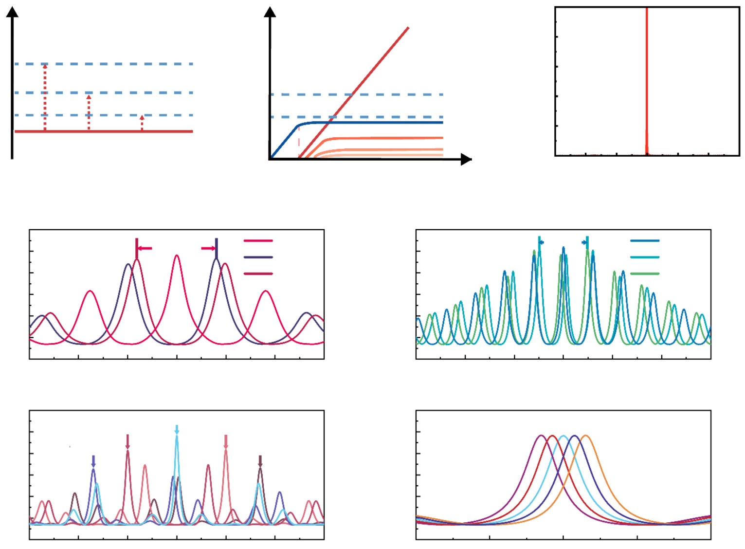
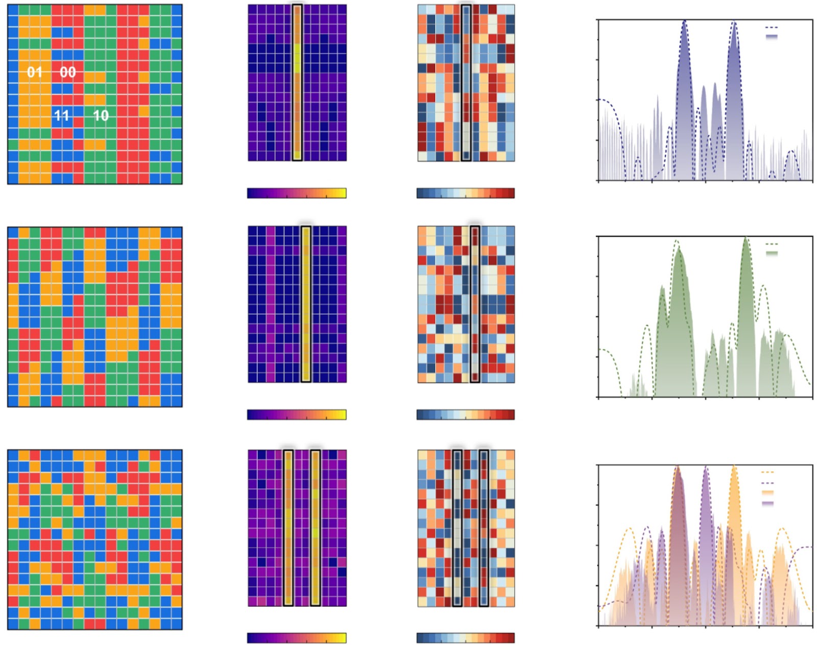
Thin-film lithium niobate (TFLN) has emerged as a promising platform for integrated photonics due to its strong electro-optic and nonlinear properties. However, on-chip tunable lasers essential for optical communications, sensing, metrology, and quantum technology remain constrained by limited tuning range or precision, often requiring complex control strategies. This work demonstrates a hybrid integrated electro-optically tunable narrow-linewidth III-V laser on TFLN, achieving a tuning range of ~51.8 nm, an intrinsic linewidth of ~1.21 MHz, and a tuning precision of ~0.03 nm. The external cavity uniquely combines highly reflective Sagnac mirrors and a series of unbalanced interferometers, providing a spectral response that favors single-longitudinal-mode narrow-linewidth lasing. Experimental results show a maximum on-chip power of 102.7 μW at 1551.69 nm, a side-mode suppression ratio of 39.65 dB, and continuous tuning range of ~3.5 pm. The laser operates mode-hop-free over long periods, with a DC voltage tuning range of −30 V to +30 V. The external cavity, built exclusively on single-mode-waveguide-based photonic structures, ensures fundamental-mode propagation, enhancing stability and relaxing fabrication tolerances. The reformulated theory of semiconductor lasers provides design insights for hybrid integrated lasers and on-chip self-injection locked lasers. This work advances the development of high-precision, wide-range tunable lasers for next-generation photonic systems.

A Hybrid Integrated High-Precision Tunable Semiconductor Laser
Graphical Abstract
Original ResearchVol. 32, Issue 1 • pp. 100-112DOI: 10.29026/oea.2026.250218Jan 15, 2026

Modelling-Guided Inverse Design Strategy for Semitransparent Perovskite Photovoltaics with Customized Colors

Authors: Seok-Beom Seo, Rira Kang, Eun-Joo Lee, So-Yeon Ju, Min Jae Lee, Byunghong Lee, Sun-Kyung Kim

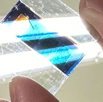
Urban architects increasingly seek solar windows that deliver both energy generation and aesthetic value. However, existing color-engineering strategies rely on absorptive metal layers or lack control over the achievable colors. Here, we present a modelling-guided inverse design strategy that integrates an all-dielectric (ZnS/MgF2) multilayer into semitransparent perovskite photovoltaics, enabling user-defined colors with minimal spectral loss. Leveraging an active learning algorithm, we mapped the attainable color gamut for ZnS/MgF2-coated devices with distinct perovskite absorber thicknesses and average visible transmittance (AVT) values. As a representative case, a device with a 110 nm-thick absorber on glass or polyethylene terephthalate (PET), initially exhibiting a reddish-brown tint, was transformed into vivid cyan using a 600 nm-thick all-dielectric multilayer. This tuning retained high AVT—6.5% on glass and 5.3% on PET—while enhancing power conversion efficiency by 20.9% and 10.4%, respectively. Real-world imaging confirmed enhanced aesthetics with see-through visibility, underscoring the practical potential of the inverse-design framework. Moreover, this approach is readily transferable to other thin film photovoltaics, providing a versatile route toward color customizable, transmittance-tunable, and high-efficiency solar windows for buildings, vehicles, and wearable electronics.

Modelling-Guided Inverse Design Strategy for Semitransparent Perovskite Photovoltaics with Customized Colors
Graphical Abstract
Original ResearchVol. 32, Issue 1 • pp. 100-112DOI: 10.29026/oea.2026.250150Jan 15, 2026

Fast Step Heterodyne Light-Induced Thermoelastic Spectroscopy Gas Sensing Based on a Quartz Tuning Fork with High-Frequency of 100 kHz

Authors: WANG Yuanzhi, HE Ying, QIAO Shunda, LIU Xiaonan, ZHANG Chu, DUAN Xiaoming, MA Yufei

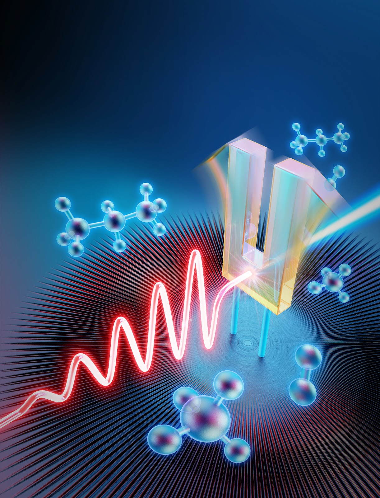
This study presents the first demonstration of a fast step heterodyne light-induced thermoelastic spectroscopy (SH-LITES) sensor utilizing a high-frequency quartz tuning fork (QTF) with a resonant frequency of approximately 100 kHz. The theoretical basis of heterodyne LITES (H-LITES) signal generation is analyzed, and an acetylene (C2H2) H-LITES sensor is constructed to evaluate performance. Comparative experiments between the high-frequency QTF and a standard commercial QTF (resonant frequency ~32.768 kHz) reveal that the high-frequency QTF achieves a tenfold faster response time, with a measurement cycle of 33 ms—90% shorter than commercial counterparts. The proposed SH-LITES technique further reduces the scanning time to 15 ms, representing the shortest LITES measurement time reported to date. To validate dynamic gas detection capabilities, an H2O-LITES system integrating both QTF types is employed for real-time monitoring of H2O concentration during various respiration patterns. Results demonstrate that SH-LITES more accurately captures rapid H2O concentration fluctuations during respiration, outperforming the commercial QTF-based H-LITES sensor in fast-response scenarios. These findings establish a new benchmark for high-speed trace gas sensing with potential applications in combustion diagnostics, healthcare monitoring, and environmental surveillance.

Fast Step Heterodyne Light-Induced Thermoelastic Spectroscopy Gas Sensing Based on a Quartz Tuning Fork with High-Frequency of 100 kHz
Graphical Abstract
Original ResearchVol. 32, Issue 1 • pp. 100-112DOI: 10.29026/oea.2026.250323Jan 15, 2026

Integrated Optical Fiber Devices: A Comprehensive Review of In-Fiber Photonic Integration

Authors: JIN Wei

Photonic integration, which incorporates multiple passive and/or active photonic components such as waveguides, modulators, lasers and detectors to form a functional circuitry on a single chip, has experienced exciting development. It enables manipulation of light with enhanced functionality, reduced form factor, and increased efficiency over bulky optical systems, with potential for applications in telecommunications, sensing, artificial intelligence, and quantum systems. In parallel, there is active research on photonic integration in an optical fiber platform. Optical fibers have been the backbone of our information society for several decades, and the field continues to develop. Beyond novel photonic crystal, photonic bandgap, and anti-resonant optical fibers, one area of significant development is the integration of novel structures and materials into optical fibers to achieve more functionalities. Examples include lab-in-fiber or lab-on-fiber technologies for biomedical applications, integration of two-dimensional and gas-phase materials with optical fibers for light manipulation, and semiconductor materials for nonlinear photonic applications. Recently, a review paper on three-dimensional integrated optical fiber devices was published in Opto-Electronics Technology. The review covers the concept and historic background of photonic integration in optical fibers, expansion of functionality by two- and three-dimensional structural modifications and material integrations, and a summary and future outlook. It includes methods such as direct fiber-drawing, side and end-face polishing, chemical etching, thermal splicing, diffusion, tapering and twisting, femtosecond laser micro-machining, assembly of microdevices and metasurfaces. Applications discussed include three-dimensional shaping sensing, refractive index sensing, chemical and biochemical sensing, polarizers and modulators, broadband photodetectors, beaming focusing and manipulation, OCT imaging, spectral filtering, vortex beam generation, and optical microfluidic devices. The field is still developing, with future directions including miniaturization of three-dimensional optical devices, distributed sensing units seamlessly integrated with optical fiber systems, optoelectronic hybrid chip and fiber integration, and integrating multifunctional photonic components into a slender optical fiber for biomedical applications.

Integrated Optical Fiber Devices: A Comprehensive Review of In-Fiber Photonic Integration
Graphical Abstract
Original ResearchVol. 32, Issue 1 • pp. 100-112DOI: 10.29026/oea.2026.250193Jan 15, 2026

Electric-field-induced second-harmonic generation

Authors: Hangkai Fan, Alexey Proskurin, Mingzhao Song, Andrey Bogdanov

Second-harmonic generation (SHG) is a fundamental second-order nonlinear optical process that coherently doubles the frequency of incident light. However, in centrosymmetric materials, the bulk second-order nonlinear susceptibility χ(2) is strictly forbidden by inversion symmetry, suppressing SHG. Applying an external electric field breaks this inversion symmetry and induces an effective second-order nonlinear response known as the electric-field-induced second-harmonic generation (EFISH) effect. This mechanism enables SHG in centrosymmetric media and provides a route for electrically tunable nonlinear nanophotonics. This review presents a comprehensive overview of the EFISH effect, covering its fundamentals, various material platforms (including bulk semiconductor crystals, ferroelectrics, van der Waals materials, and polymers), and diverse strategies for electric field engineering. We distinguish EFISH from related effects such as current-induced SHG and the quantum-confined Stark effect. Emerging applications of EFISH in tunable photonic devices, carrier dynamics probing, and nonlinear optical modulation across optical, electronic, and THz regimes are highlighted. Key challenges and prospects for the future development of electrically controlled nonlinear optical systems are outlined. The review consolidates the state of the art and provides a critical assessment of the field's trajectory.

Electric-field-induced second-harmonic generation
Graphical Abstract
Original ResearchVol. 32, Issue 1 • pp. 100-112DOI: 10.29026/oea.2026.250269Jan 15, 2026

Timeshare Surface-Enhanced Raman Scattering Platform with Sensitive and Quantitative Mode

Authors: DING Qianqian, CHEN Xueyan, JIA Yunlu, LIU Hong, ZHANG Xiaochen, CHENG Ningtao, YANG Shikuan

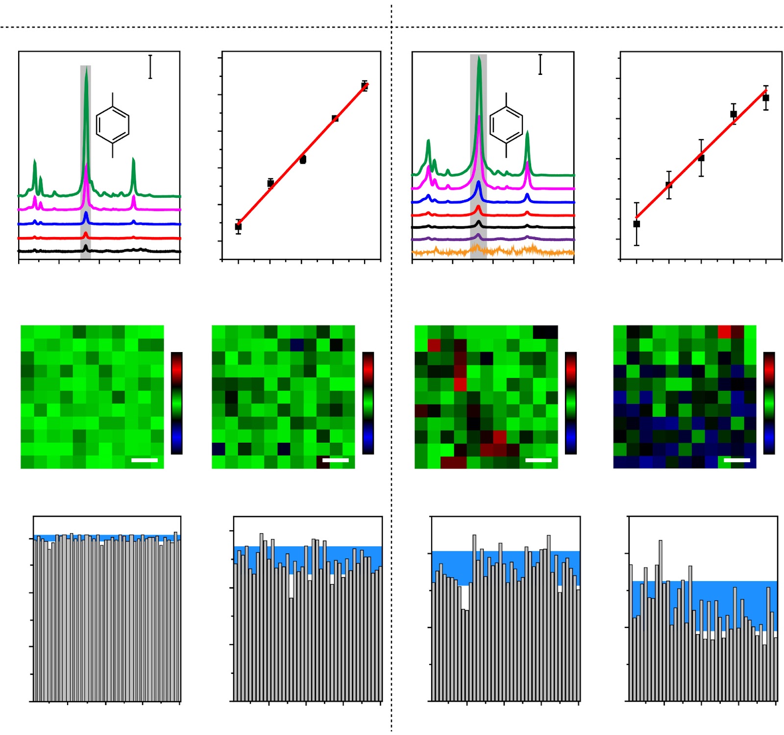
Surface-enhanced Raman scattering (SERS) substrates face an intrinsic trade-off: the ultrasensitive hottest spots required for single-molecule detection amplify analyte signals by orders of magnitude, causing each molecule to be miscounted as hundreds during quantification. This study demonstrates a timeshare SERS platform that circumvents this contradiction by dynamically toggling between quantitative and sensitive modes on demand. The platform is constructed by transferring a monolayer gold nanosphere film onto an elastic hydrogel substrate. The hydrogel's volume change adjusts the inter-nanosphere distance, reversibly controlling the formation or extinction of SERS hottest spots without altering the spatial distribution of analyte molecules. In the absence of hottest spots, the platform exhibits strong quantification capability; when equipped with a substantial number of hottest spots, it achieves ultrahigh sensitivity. The authors demonstrate quantitative and ultrasensitive detection of various analyte molecules using the respective modes. This approach opens a route to designing SERS substrates that simultaneously offer high sensitivity and robust quantification, addressing a long-standing bottleneck in trace detection for analytical chemistry, environmental monitoring, food safety, and biomedical diagnostics.

Timeshare Surface-Enhanced Raman Scattering Platform with Sensitive and Quantitative Mode
Graphical Abstract
Original ResearchVol. 32, Issue 1 • pp. 100-112DOI: 10.29026/oea.2026.250149Jan 15, 2026

High-fidelity full-color self-interference incoherent digital holography via quarter-wave geometric phase optics

Authors: Jae-Won Lee, Jin-Hyeok Seo, Jung-Yeop Shin, Jing-Wen Bu, Kihong Choi, Keehoon Hong, Hak-Rin Kim

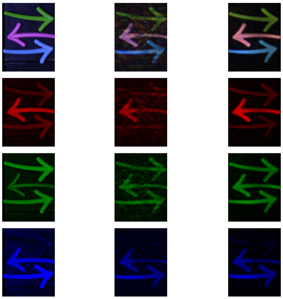
Self-interference incoherent digital holography (SIDH) enables three-dimensional imaging under broadband illumination without a reference arm, but conventional implementations using half-waveplate (HWP)-based geometric phase (GP) lenses suffer from triple-wavefront polarization interference. This interference arises from chromatic dispersion in phase retardation, producing color-dependent artifacts that degrade full-color reconstruction fidelity. We introduce a quarter-waveplate (QWP)-based GP lens architecture that suppresses the parasitic third wavefront by exploiting the non-diffracted beam as the reference, yielding stable dual-wavefront modulation. The resulting phase-encoded polarization interference patterns remain spectrally consistent across red, green, and blue channels. Experimental validation demonstrates substantial noise suppression and improved full-color image fidelity, quantified through channel-specific noise analysis and structural similarity metrics. The system retains a simplified optical configuration without active polarization control, supporting compact integration and cost-effective fabrication. These results establish the QWP-GP SIDH architecture as a viable route for portable, real-time digital holographic 3D imaging, with potential scalability in augmented reality, optical diagnostics, and spectral holography.

High-fidelity full-color self-interference incoherent digital holography via quarter-wave geometric phase optics
Graphical Abstract
Original ResearchVol. 32, Issue 1 • pp. 100-112DOI: 10.29026/oea.2026.250229Jan 15, 2026

Ambient-energy-driven space-time-coding metasurface for space-frequency-division multiplexing wireless communications

Authors: TIAN Han Wei, SONG Chao, WANG Dong Jie, ZHU Qian, CUI Tie Jun, JIANG Wei Xiang

Programmable metasurfaces have demonstrated potential for dynamic electromagnetic wave manipulation, yet their large-scale deployment is constrained by high communication capacity demands and stringent energy requirements. This work presents an ambient-energy-driven space-time-coding metasurface that achieves space-frequency-division multiplexing while operating self-sufficiently via integrated solar energy harvesting. The metasurface dynamically controls multiple frequencies and spatial propagation directions of reflected waves, enabling four independent communication channels. A four-channel wireless communication prototype transmitted four distinct images to separate user terminals simultaneously and in real time, with energy consumption per bit markedly lower than conventional programmable metasurfaces. The shared-aperture design integrates ambient solar harvesting and low-power programmable elements, eliminating external power supplies. Experimental validation confirms independent multichannel operation with low inter-channel interference. This platform merges ambient energy harvesting, multidimensional microwave manipulation, and direct information modulation on a single physical layer, offering a cost-effective, energy-efficient, and environmentally friendly pathway for high-capacity wireless communications. The results establish a foundational architecture for self-powered reconfigurable intelligent surfaces in next-generation networks.

Ambient-energy-driven space-time-coding metasurface for space-frequency-division multiplexing wireless communications
Graphical Abstract
Original ResearchVol. 32, Issue 1 • pp. 100-112DOI: 10.29026/oea.2026.250271Jan 15, 2026

Fiber-optic photoacoustic enables targeted neuromodulation and stress reduction in mice

Authors: PENG Yuan Bo

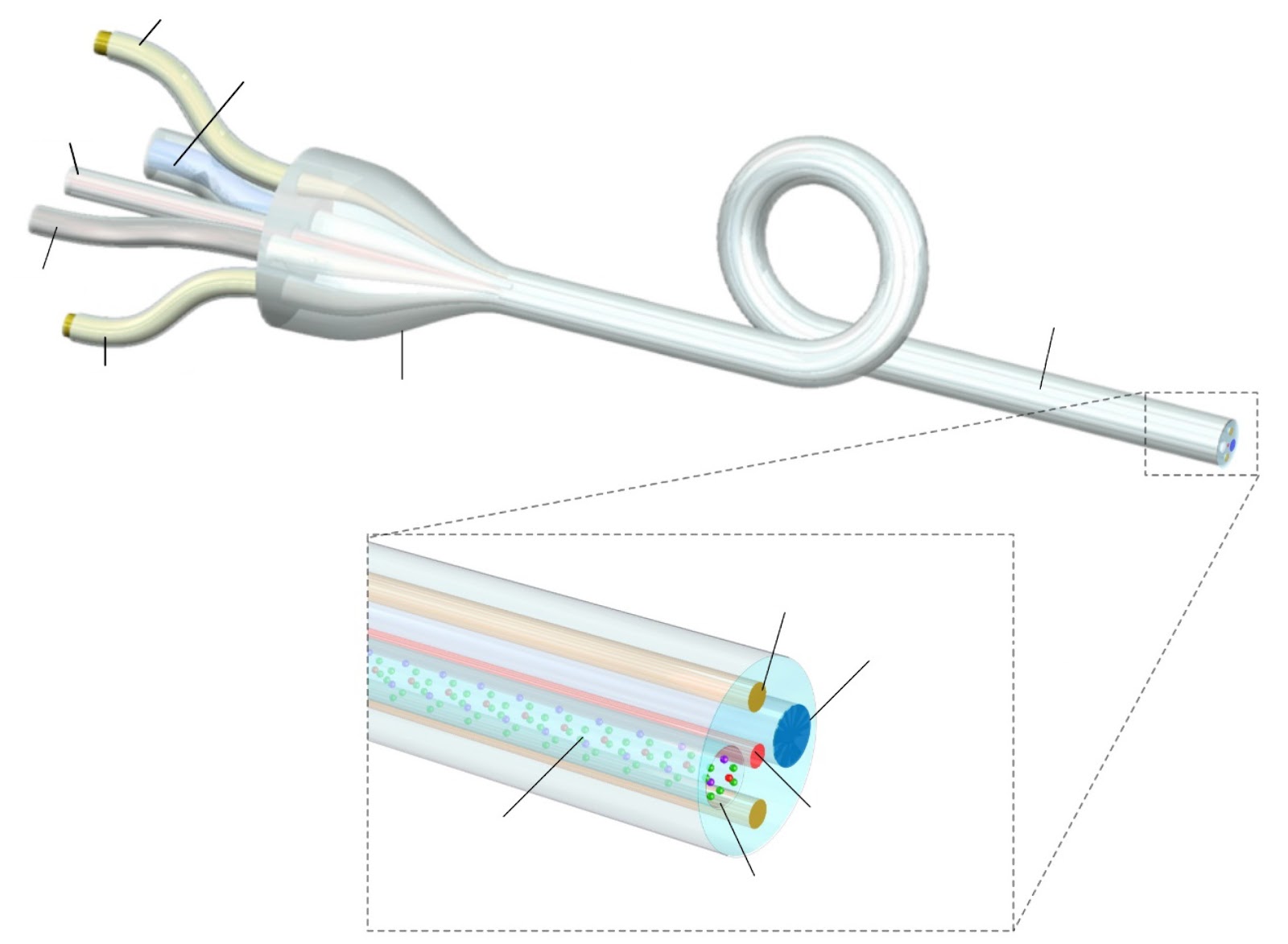
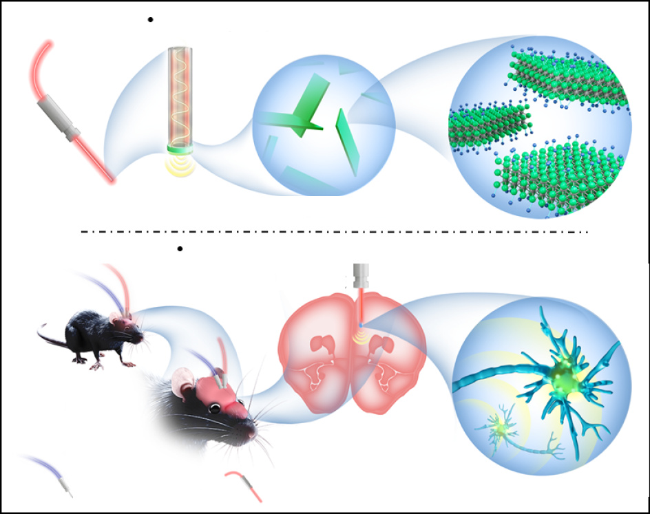
Ultrasound neuromodulation offers a non-invasive approach to modulate neural activity in the central nervous system, yet precise, minimally invasive devices capable of targeted stimulation remain limited. A 200 µm diameter fiber-optic photoacoustic emitter (FPE) was developed, coated with a MXene (Ti3C2Tx) and polydimethylsiloxane composite to generate controllable, broadband ultrasonic waves with high spatial precision. Using this FPE to stimulate the medial prefrontal cortex in mice, it was observed marked alleviation of acute social defeat stress-induced emotional stress, evidenced by reduced anxiety-like behavior and increased social interaction. This approach enables near-field, broadband, and tunable ultrasound neuromodulation with potential applications in treating neuropsychiatric disorders involving emotional regulation. The FPE leverages the excellent photothermal stability of Ti3C2Tx under repeated near-infrared (1064 nm) radiation, allowing continuous laser pulses that consistently emit ultrasound. The generated ultrasound can achieve pressures up to several MPa and bandwidths exceeding 20 MHz, supporting detailed imaging and discrimination of tissue microstructure. By integrating in situ ultrasound generation at the fiber tip, shrinking the source-to-target distance to hundreds of micrometers, and naturally reducing far-field energy accumulation and off-target risks, this work demonstrates a highly miniaturized, directional, and broadband ultrasound generator for imaging and sensing applications, particularly in minimally invasive procedures. The study, published in Opto-Electronic Science, represents a significant advancement in targeted neuromodulation for emotional stress modulation.

Fiber-optic photoacoustic enables targeted neuromodulation and stress reduction in mice
Graphical Abstract
Original ResearchVol. 32, Issue 1 • pp. 100-112DOI: 10.29026/oea.2026.250267Jan 15, 2026

Scene-Level Passive Polarization 3D Imaging

Authors: WANG Xin, HAN Pingli, LUO Xiyuan, LIU Qianqian, ZHANG Tong, DONG Xue, XIANG Meng, LIU Jinpeng, LIU Yanyan, LIU Fei

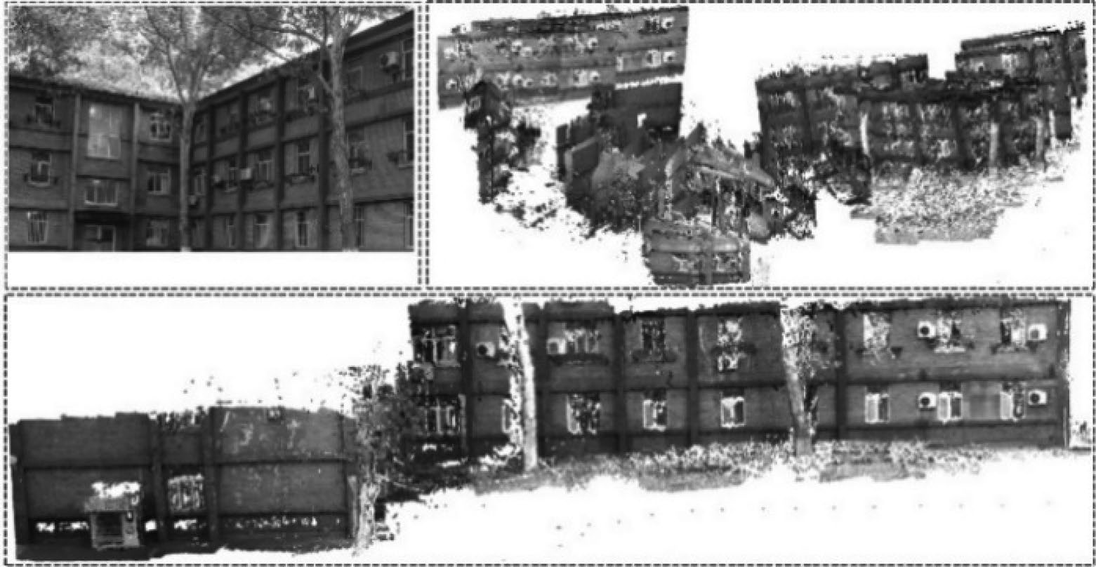
Scene-level passive 3D imaging under natural conditions remains a critical unmet need, as established techniques such as structured light, LiDAR, and active stereo rely on controlled illumination and scanning, limiting their applicability to large, dynamic outdoor environments. Passive polarization 3D imaging offers inherent advantages for long-range, high-precision reconstruction but is fundamentally impeded by two obstacles: the π ambiguity of the azimuth component of surface normals and the discontinuity of multiple targets within a scene. This study introduces a scene-level passive polarization 3D imaging method that integrates binocular stereo vision with polarization cues. The reconstruction of discontinuous targets is formulated as a minimization problem, where pixel-level normal directions from polarization and absolute scale information from binocular stereo serve as mutual constraints for iterative optimization. This framework resolves the discontinuity challenge and recovers true depth. A scale normalization strategy globally aligns multi-view measurement data, eliminating inter-frame scale inconsistencies that hinder dynamic reconstruction. Multi-frame point cloud fusion yields the final scene-level 3D structure. Experimental validation on natural field scenes demonstrates robust, wide-scene, high-accuracy passive video reconstructions with centimeter-level precision. This passive polarization stereo approach represents a significant advancement in scene-level 3D imaging, with potential applications in autonomous navigation, environmental monitoring, and cultural heritage documentation.

Scene-Level Passive Polarization 3D Imaging
Graphical Abstract
Original ResearchVol. 32, Issue 1 • pp. 100-112DOI: 10.29026/oea.2026.250265Jan 15, 2026

Shedding Light on Glucose: Tip-Enhanced Raman Scattering Achieves Complete Vibrational Fingerprint Coverage (400–3200 cm⁻¹) for Non-Invasive Metabolite Detection

Authors: Mohsen Rahmani

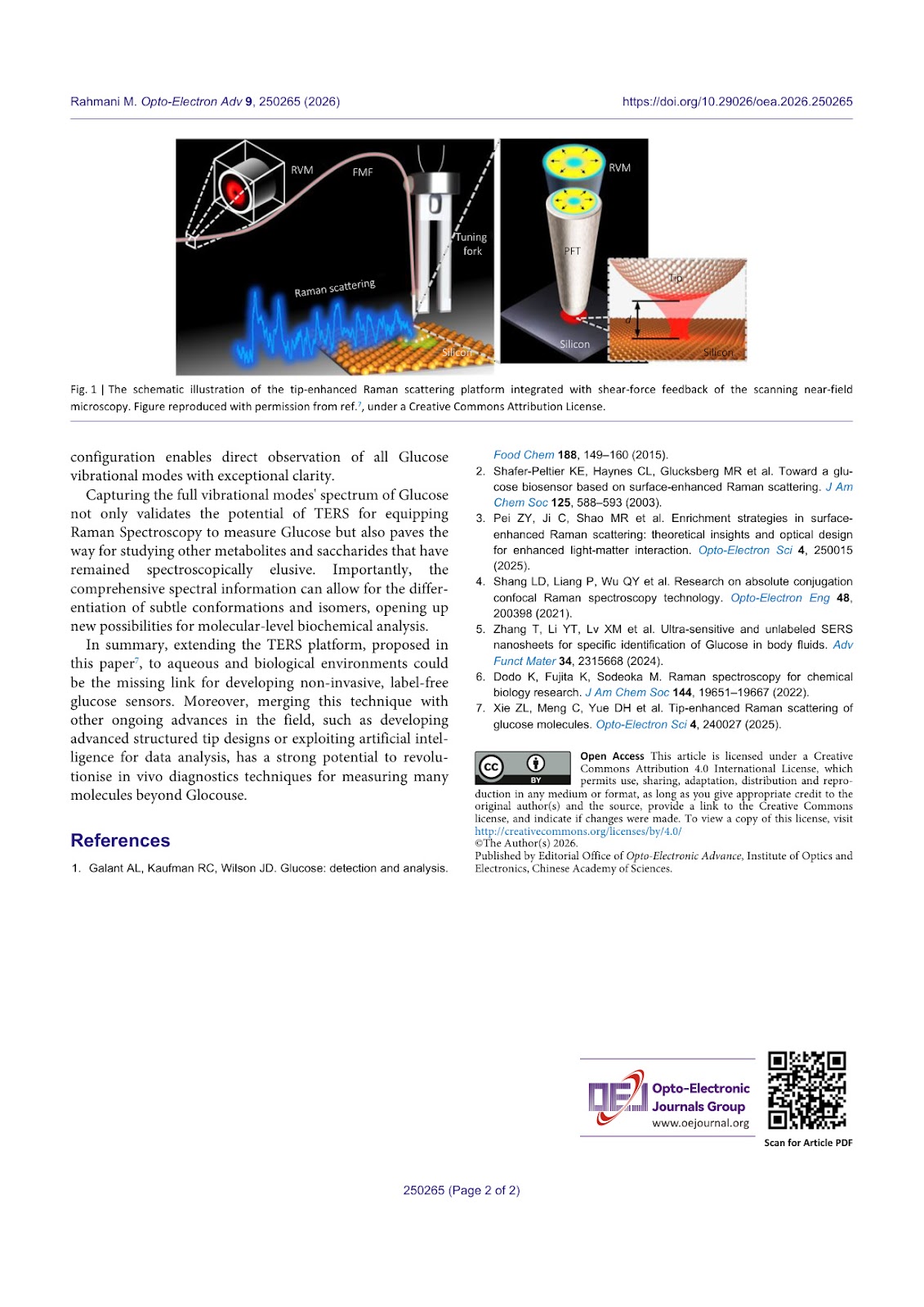
Non-invasive glucose monitoring remains a critical unmet clinical need, primarily because glucose exhibits an inherently weak Raman scattering cross-section—approximately five times smaller than that of benzene—and poor affinity for bare metal surfaces. While surface-enhanced Raman spectroscopy (SERS) can amplify weak signals, it suffers from incomplete spectral coverage and interference from linker molecules, preventing reliable comprehensive analysis. A recent study by Xie et al. published in Opto-Electronic Science demonstrates that tip-enhanced Raman scattering (TERS) can record the complete vibrational spectrum of glucose molecules across the 400–3200 cm⁻¹ Raman recording window. By combining a shear-force feedback-controlled scanning probe with a radially polarised vector beam launched through an optical fibre tip, the authors achieve strong near-field confinement and far-field background suppression. The tip concentrates a strong longitudinal electric field along its axis, maximising the localised hotspot at the apex, which boosts near-field enhancement and enables more complete vibrational fingerprints to be captured. This label-free approach overcomes the long-standing barriers of weak signal intensity and incomplete spectral coverage, establishing a viable pathway for highly sensitive metabolite detection and future in vivo biosensing applications. The work represents a significant advance in optical diagnostic techniques for diabetes management and broader clinical metabolite monitoring.

Shedding Light on Glucose: Tip-Enhanced Raman Scattering Achieves Complete Vibrational Fingerprint Coverage (400–3200 cm⁻¹) for Non-Invasive Metabolite Detection
Graphical Abstract