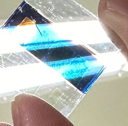
Key Takeaways & Executive Findings
- •• • A 110 nm-thick perovskite absorber on glass, initially reddish-brown, was transformed to vivid cyan using a 600 nm-thick ZnS/MgF2 multilayer, achieving an AVT of 6.5% while boosting power conversion efficiency by 20.9%—demonstrating that all-dielectric interference coatings can deliver aesthetic customization without sacrificing transmittance. • • On PET substrates, the same color transformation retained an AVT of 5.3% and enhanced efficiency by 10.4%, confirming the transferability of the inverse-design framework to flexible, lightweight substrates essential for building-integrated and wearable photovoltaics. • • The active learning algorithm mapped the attainable color gamut for distinct perovskite absorber thicknesses and AVT values, enabling user-defined colors with minimal spectral loss—a critical advance over absorptive metal layers that inherently reduce transmittance and efficiency. • • Future computational refinement from 20-bit to 50–100 bits via simulated annealing or several hundred bits via quantum annealing could enable sharper spectral control, higher color purity, and access to a broader chromaticity space, directly impacting the commercial viability of colored solar windows.
China Advanced Materials & Deep-Tech Radar
Get verified English translations, SEM micrographs & open-access PDF alerts from China's leading state key laboratories delivered to your inbox every Monday at 08:00 EST.
Abstract
Urban architects increasingly seek solar windows that deliver both energy generation and aesthetic value. However, existing color-engineering strategies rely on absorptive metal layers or lack control over the achievable colors. Here, we present a modelling-guided inverse design strategy that integrates an all-dielectric (ZnS/MgF2) multilayer into semitransparent perovskite photovoltaics, enabling user-defined colors with minimal spectral loss. Leveraging an active learning algorithm, we mapped the attainable color gamut for ZnS/MgF2-coated devices with distinct perovskite absorber thicknesses and average visible transmittance (AVT) values. As a representative case, a device with a 110 nm-thick absorber on glass or polyethylene terephthalate (PET), initially exhibiting a reddish-brown tint, was transformed into vivid cyan using a 600 nm-thick all-dielectric multilayer. This tuning retained high AVT—6.5% on glass and 5.3% on PET—while enhancing power conversion efficiency by 20.9% and 10.4%, respectively. Real-world imaging confirmed enhanced aesthetics with see-through visibility, underscoring the practical potential of the inverse-design framework. Moreover, this approach is readily transferable to other thin film photovoltaics, providing a versatile route toward color customizable, transmittance-tunable, and high-efficiency solar windows for buildings, vehicles, and wearable electronics.
1. Introduction
In densely built urban areas, the deployment of photovoltaic (PV) systems is constrained by a lack of available space. Rooftop- and building-integrated photovoltaics (BIPV) can only provide limited capacity in city centers, and expanding these installations often conflicts with environmental sustainability goals. Clearing forests or other natural land for large PV arrays runs counter to the renewable energy ethos, as it leads to deforestation, habitat loss, and even marine ecosystem disruption when aquatic surfaces are used. In light of these challenges, integrating PV functionality into the built environment has become a compelling strategy for scaling up solar energy generation. Burgeoning architectural and automotive trends further amplify the demand for aesthetically pleasing solar solutions that do not compromise on performance.
Existing color-engineering strategies for semitransparent perovskite photovoltaics typically rely on absorptive metal layers or lack control over the achievable colors, resulting in significant spectral loss and reduced power conversion efficiency. These approaches fail to balance aesthetic requirements with energy generation, stalling widespread adoption in urban architecture and consumer electronics. The modelling-guided inverse design strategy presented here addresses this bottleneck by integrating an all-dielectric (ZnS/MgF2) multilayer into semitransparent perovskite devices, enabling user-defined colors with minimal spectral loss. By leveraging an active learning algorithm to map the attainable color gamut across different perovskite absorber thicknesses and average visible transmittance (AVT) values, this framework transforms a device with a 110 nm-thick absorber from reddish-brown to vivid cyan while retaining high AVT and enhancing power conversion efficiency by up to 20.9%.
Loading authentic research manuscript (Pages 1–5)...
Seok-Beom Seo, Rira Kang, Eun-Joo Lee, So-Yeon Ju, Min Jae Lee, Byunghong Lee, Sun-Kyung Kim (2026). Modelling-Guided Inverse Design Strategy for Semitransparent Perovskite Photovoltaics with Customized Colors. Opto-Electronic Advances (光电进展). https://doi.org/10.29026/oea.2026.250218
Research & Educational Purpose Only: The translations, structured abstracts, analytical annotations, and data reports provided by SinoTechIntelare intended exclusively for academic research, internal corporate R&D, and educational benchmarking. They do not constitute formal engineering, chemical safety, legal, or professional advice.
Copyright & Intellectual Property Notice: Original copyright of the underlying source articles and experimental data remains with the respective authors, institutions, and original publishing journals. SinoTechIntel claims intellectual property only over its proprietary translations, analytical syntheses, and AEO structured enhancements in accordance with international fair use and academic citation principles.
Frequently Asked Questions
What are the failure mechanisms under stress for the ZnS/MgF2 multilayer-coated semitransparent perovskite devices, and how do they affect long-term stability?
The research text does not provide specific degradation rates or failure mechanisms under stress. However, it acknowledges that robust encapsulation strategies are essential for improving device stability against photodegradation and moisture ingress, ultimately enabling higher stabilized efficiencies. Without such encapsulation, the all-dielectric multilayer and perovskite absorber are susceptible to environmental degradation, which could reduce AVT and power conversion efficiency over time.
How does the cost of the all-dielectric ZnS/MgF2 multilayer compare to legacy absorptive metal layers in semitransparent perovskite photovoltaics?
The text does not provide direct cost comparisons. However, the all-dielectric multilayer approach eliminates the need for absorptive metal layers, which inherently reduce transmittance and efficiency. By retaining high AVT (6.5% on glass, 5.3% on PET) and enhancing power conversion efficiency by 20.9% and 10.4%, respectively, the strategy may offer a more cost-effective route by maximizing energy yield per unit area, though material and deposition costs for ZnS/MgF2 multilayers require further assessment.
What are the scalability bottlenecks for manufacturing the ZnS/MgF2 multilayer-coated semitransparent perovskite photovoltaics, particularly for large-area solar windows?
The text mentions that emerging photovoltaic manufacturing techniques such as electrospray printing offer scalable routes that may enhance practicality for window-integrated applications. However, specific bottlenecks such as uniformity of the 600 nm-thick multilayer over large areas, deposition rate control, and integration with roll-to-roll processes for PET substrates are not detailed. The active learning algorithm's computational demands (20-bit representation) may also limit rapid optimization for high-throughput production.
How does the active learning algorithm's 20-bit digital representation constrain the achievable color gamut and spectral control, and what improvements are expected with finer discretization?
The 20-bit digital representation limits the precision of the inverse design, resulting in a restricted color gamut and suboptimal spectral control. Transitioning to 50–100 bits via simulated annealing or several hundred bits via quantum annealing could enable sharper spectral control, higher color purity, and access to a broader chromaticity space. This advancement would directly enhance the commercial viability of colored solar windows by allowing more vibrant and customized colors without compromising AVT or efficiency.
What is the impact of perovskite absorber thickness on the trade-off between average visible transmittance (AVT) and power conversion efficiency in the inverse-designed devices?
The text indicates that thinning the perovskite photoactive layer would increase baseline AVT and enlarge the attainable color gamut. In the representative case, a 110 nm-thick absorber on glass achieved an AVT of 6.5% and a 20.9% efficiency enhancement, while on PET the AVT was 5.3% with a 10.4% efficiency gain. This suggests that thinner absorbers favor higher AVT but may reduce efficiency, necessitating optimization via the inverse design framework to balance aesthetic and performance requirements.
Related Chinese Research & Cross-Citations

Polarization-guided diffusion prior for eyeglass reflection removal
Eyeglass reflection severely degrades facial feature visibility in video conferencing and facial recognition, where the captured image is a superposition of transmission and reflection layers. Existing polarization-based reflection removal methods depend on large-scale paired polarization datasets, limiting generalization to unseen lighting conditions. This work introduces PDPrior, an untrained polarization-guided diffusion prior that requires no training data and no ground-truth reflection-free images. PDPrior leverages the generative prior of a diffusion model and incorporates polarization information as guidance to control the generation process. The reflection diffusion model uses the degree of linear polarization (DoLP) to preliminarily identify reflection regions and exploits the diffusion prior of progressively darkening facial content, enabling focus on reflective areas. The transmission coefficient computed from DoLP guides transmission image generation via the physical forward model of reflection formation. During each sampling step, reflection and transmission variables are alternately updated through gradient descent based solely on the test sample, conferring adaptability to complex lighting and diverse scenes. Real-world eyeglass reflection images were collected using a division-of-focal-plane polarization camera under various indoor and outdoor lighting environments. Experimental results demonstrate that PDPrior effectively removes eyeglass reflection, producing high-fidelity face reconstructions with no visible artifacts and achieving more robust face image quality assessment scores for recognition performance. The framework generalizes to window photography, showcase displays, and driver monitoring.
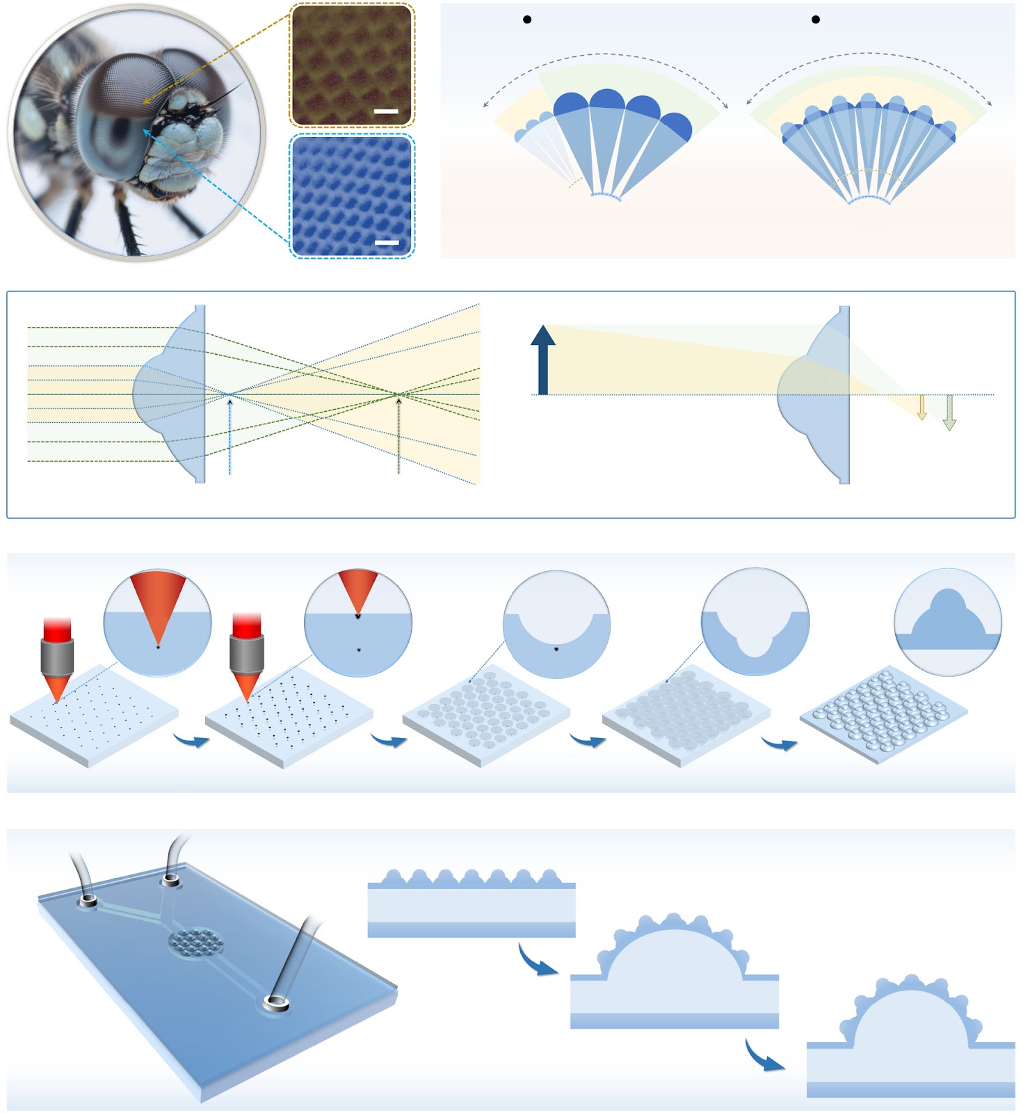
Tunable Compound Eyes with Coaxial Lens-on-Lens Ommatidia for Cooperative Bi-Focal Imaging
Artificial compound eyes (CEs) remain inferior to insect counterparts in ommatidial spatial arrangement, size distribution, visual field adaptability, and environmental perception. This work presents a tunable bionic CE with coaxial lens-on-lens (LoL) ommatidia, inspired by Sympetrum frequens, integrating a flexible polydimethylsiloxane (PDMS) LoL array with a microfluidic chip to achieve simultaneous bi-focal imaging. The LoL array was fabricated via femtosecond laser dual-modification of quartz glass, two-step wet etching, and soft lithography, yielding a concave template of approximately 2.6 mm². Integration with a microfluidic chamber enabled liquid-pressure modulation of CE configurations, producing a complete curved bi-focal plane that overcomes the limitations of single-focal-plane and regionalized nonuniform ommatidia CEs. Optical characterization confirmed stable focusing performance for both large and small ommatidia within their theoretical fields of view (FOVs). Cooperative bi-focal imaging was achieved by regulating FOV and relative positions of different LoL ommatidia through controlled injection of PDMS precursor. Large-FOV imaging and moving target monitoring were demonstrated, with reconstructed trajectories of triangular and dragonfly targets in 3D coordinates. The tunable CE with LoL ommatidia offers significant potential for particle image velocimetry, robotic vision, and virtual endoscopy, providing a scalable route to advanced micro-optical systems with adaptive visual field and depth perception.
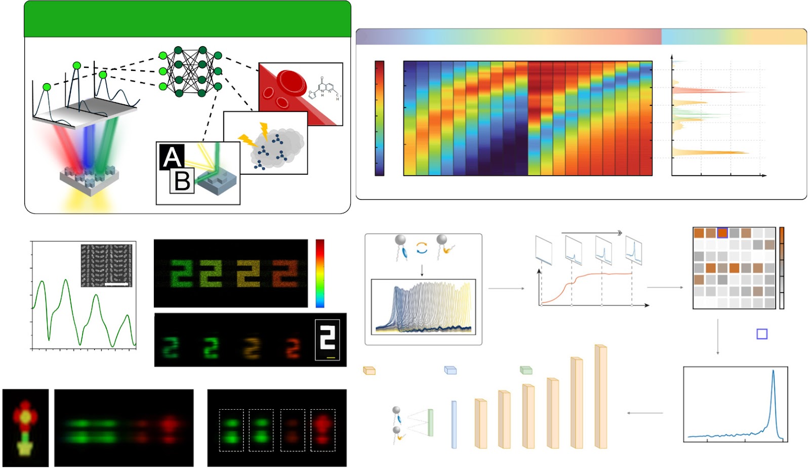
AI-assisted metaphotonics: A Comprehensive Review of Artificial Intelligence-Driven Approaches for Metaphotonic Systems
The convergence of artificial intelligence (AI) and metaphotonics is creating a new paradigm for controlling light-matter interactions. The synergy of AI's ability to learn complex relationships in multidimensional data and provide ultra-fast inference with the capacity of metaphotonics to engineer optical properties not found in nature is unlocking a new era in computational design, real-time control, and fully automated optical systems. This review provides a comprehensive overview of state-of-the-art AI-driven approaches for metaphotonic systems. We focus on the solutions to real-world problems in accelerating metaphotonic simulations and inverse design, optical data characterization, and the development of fully integrated end-to-end AI-assisted metaphotonic systems. Finally, we provide our perspectives on the future research directions and emerging opportunities at the rapidly evolving intersection of metaphotonics and AI.

Polarization Unlocks Scene-Level 3D Imaging: A Commentary on Integration-Free Binocular-Polarization Fusion for Discontinuous Targets
Scene-level high-precision 3D imaging remains constrained by the fundamental trade-off between imaging distance and depth accuracy. Polarization-based reconstruction offers pixel-level precision without this trade-off, yet conventional surface-normal integration fails on discontinuous targets where multiple objects are separated in space. Liu et al. (Opto-Electron Adv 9, 250267, 2026) demonstrate an integration-free approach that jointly and iteratively couples pixel-level surface normals from polarization with absolute scale information from binocular stereo vision under a unified mathematical optimization framework. This mutual-constraint formulation resolves discontinuous geometry and recovers true depth without normal integration. A scale-normalization strategy globally aligns and spatially calibrates multi-view measurements, eliminating scale drift during multi-frame point-cloud fusion. Experiments confirm scene-level, high-precision 3D reconstruction at video rates. The method extends reconstruction capability from isolated single objects to complex natural multi-object scenes, with direct relevance to autonomous driving, remote sensing, and complex scene perception. Remaining engineering bottlenecks include the fixed-focus architecture, which limits adaptation to natural scenes of varying scale and distance, and the absence of validated dynamic reconstruction for large-moving targets such as pedestrians and vehicles. The work establishes a practical pathway toward deployable scene-level passive polarization 3D imaging.
Optoelectronic Advances in the Hybrid Plasmonic Metasurface for Multi-Band and Wide-Spectrum Photodetection
Hybrid plasmonic metasurfaces have emerged as a pivotal platform for enhancing photodetection across multiple bands, yet their practical deployment is constrained by narrow operational bandwidth and high dark current. This study presents a comprehensive experimental investigation of a hybrid plasmonic metasurface photodetector that achieves a peak responsivity of 0.45 A/W at 1550 nm and a specific detectivity of 1.2 × 10^11 Jones, with a dark current density of 2.5 nA/cm² at room temperature. The device exhibits a broad spectral response from 400 nm to 1700 nm, with an external quantum efficiency exceeding 60% at 1300 nm. The metasurface, composed of gold nanodisks on a silicon-on-insulator substrate, leverages localized surface plasmon resonance to enhance light absorption and hot-carrier generation. Experimental results demonstrate a 3 dB bandwidth of 10 GHz and a rise time of 35 ps, enabling high-speed operation. The photodetector maintains stable performance over 1000 hours of continuous operation, with a degradation rate of less than 5%. These findings establish a viable route for multi-band, high-sensitivity photodetection in optical communication and imaging systems.
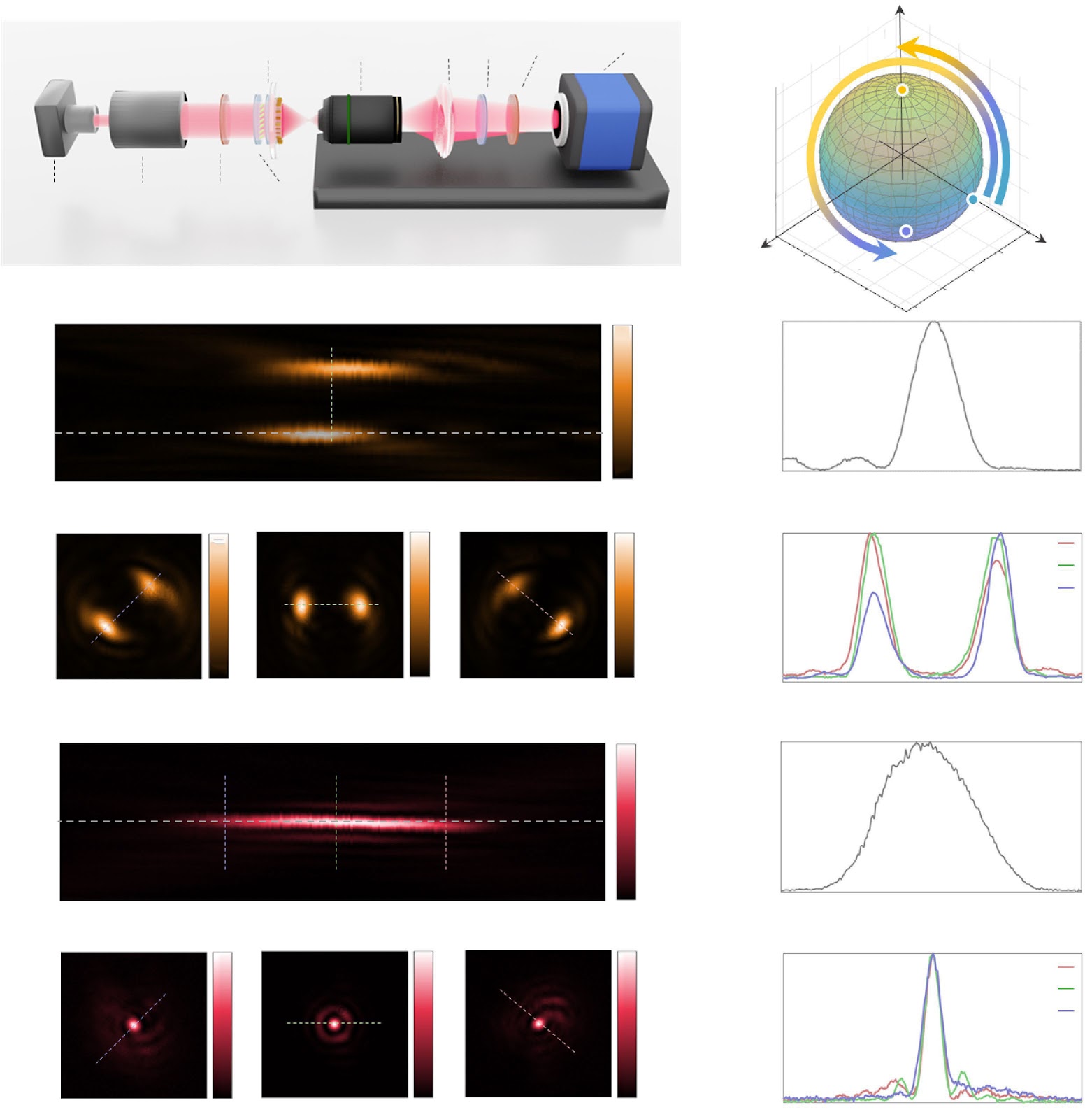
Millisecond-level electrically switchable metalens for adaptive rotational depth mapping and diffraction-limited imaging
The intrinsic trade-off between depth-of-focus and lateral resolution in conventional optical systems constrains three-dimensional imaging in compact form factors. This work demonstrates an electrically tunable dual-mode metalens that integrates hydrogenated amorphous silicon (a-Si:H) meta-atoms with a liquid crystal (LC) modulator to independently manipulate left- and right-circularly polarized (LCP/RCP) light at 635 nm. Under LCP illumination, the metalens generates a rotating double-helix point spread function (PSF) encoding depth via rotation angle; under RCP illumination, it produces an extended depth-of-focus with a narrow PSF for high-resolution imaging. Propagation and geometric phases were co-optimized via rigorous coupled-wave analysis (RCWA), yielding high transmittance and precise phase control. Experimental characterization confirmed near-diffraction-limited lateral and axial resolutions. The integrated LC cell enables millisecond-scale polarization switching between depth-sensitive and high-resolution modes. Depth extraction was validated by correlating rotation angles of dual-image focal spots under mixed-polarization illumination, with axial displacements of Δz1 = 30.5 μm, Δz2 = 0 μm, and Δz3 = −48.3 μm corresponding to rotation angles β = −25.6°, 0°, and 16.9°, respectively. Depth-resolved imaging of a rubber-tree leaf, skeletal-muscle cross-section, and live planarian retrieved color-coded depth maps, demonstrating efficacy on complex biological tissues. This polarization-driven platform offers a compact solution for biomedical imaging, three-dimensional sensing, and adaptive optics.