SinoTechIntel Academic Portal
🏛️ Indexed Academic JournalImpact Factor: 3.8

Journal of Semiconductors (半导体学报 - 中国科学院半导体研究所)

Authoritative peer-reviewed journal in materials science, metallurgy, chemistry and engineering technologies: Journal of Semiconductors (半导体学报 - Viện Bán dẫn CAS)

Total Research Papers: 115
Access: 100% Free Open Access
Browse by Publication Year & VolumeReset All Filters ✕

Published Research PapersFiltered: Year 2025 • Vol. 32 • 6

Showing 8 of 115 peer-reviewed papers with full Graphical Abstracts.

Original ResearchVol. 32, Issue 6 • pp. 100-112DOI: 10.1088/1674-4926/25060003Jan 15, 2025

Challenges, development and future of silica abrasives in chemical mechanical polishing derived from past six decades

Authors: WU Zuozuo, CHENG Jinglin, YU Zhiguo, ZHOU Wei, LI Yangjian, CAO Jianwei, SUN Wei, YUAN Shuai, YANG Deren

Chemical mechanical polishing (CMP) serves as an indispensable process for achieving global planarization in semiconductor manufacturing, especially as integrated circuit (IC) technology advances to sub-7 nm nodes, where atomic-level surface flatness becomes crucial. Silica abrasives, which account for over 90% of the abrasive market in advanced CMP processes, operate not through simple mechanical grinding but through a key "chemical-mechanical synergistic" mechanism: chemically softening the wafer surface, then mechanically removing the softened layer to expose a new surface, which is further softened and removed, repeating this cycle to produce a smooth wafer. Despite their prevalence, conventional silica abrasives still face challenges, including relatively low material removal rate (MRR), a tendency to agglomerate, leading to poor dispersion and surface defects, and limitations in achieving ultimate surface uniformity. Significant progress has been made to address these issues. Development has progressed from simple spherical particles to complex structural designs (such as mesoporous, hollow, and raspberry-shaped structures) to enhance slurry transport and mechanical action. Surface chemical modifications (e.g., using amino or polymer groups) can improve dispersion stability and reduce scratching. Furthermore, composites with other materials (e.g., ceria, polymers) and precise control of particle size distribution are key to enhancing performance. These innovative approaches have yielded significant performance gains. State-of-the-art slurries have demonstrated the ability to achieve surface roughness below 0.1 nm RMS. The development of silica abrasives is increasingly focused on sustainability and smart manufacturing. A prominent direction is the design of biodegradable abrasives that disintegrate after use, thereby simplifying post-chemical mechanical polishing (CMP) cleanup and minimizing environmental impact—an approach fully aligned with green manufacturing principles. This review systematically summarizes the progress of silica abrasives for CMP over the past 60 years. This summary provides theoretical insights and forward-looking strategies to overcome the current limitations of abrasive technology. We believe this review will be helpful in advancing the field of CMP abrasives.
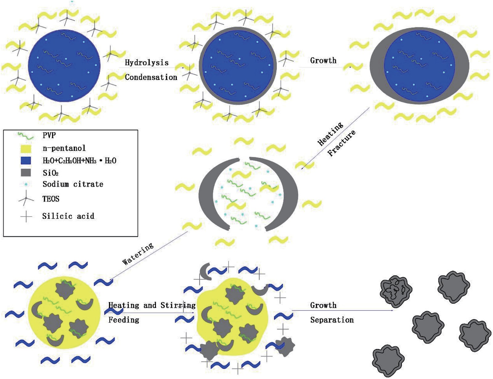
Challenges, development and future of silica abrasives in chemical mechanical polishing derived from past six decades
Graphical Abstract
Original ResearchVol. 32, Issue 6 • pp. 100-112DOI: 10.1088/1674-4926/25060030Jan 15, 2025

Effects of cell topology and JFET width on depletion layer of SiC MOSFET

Authors: Bofeng Zheng, Houcai Luo, Huan Wu, Jingping Zhang, Xianping Chen

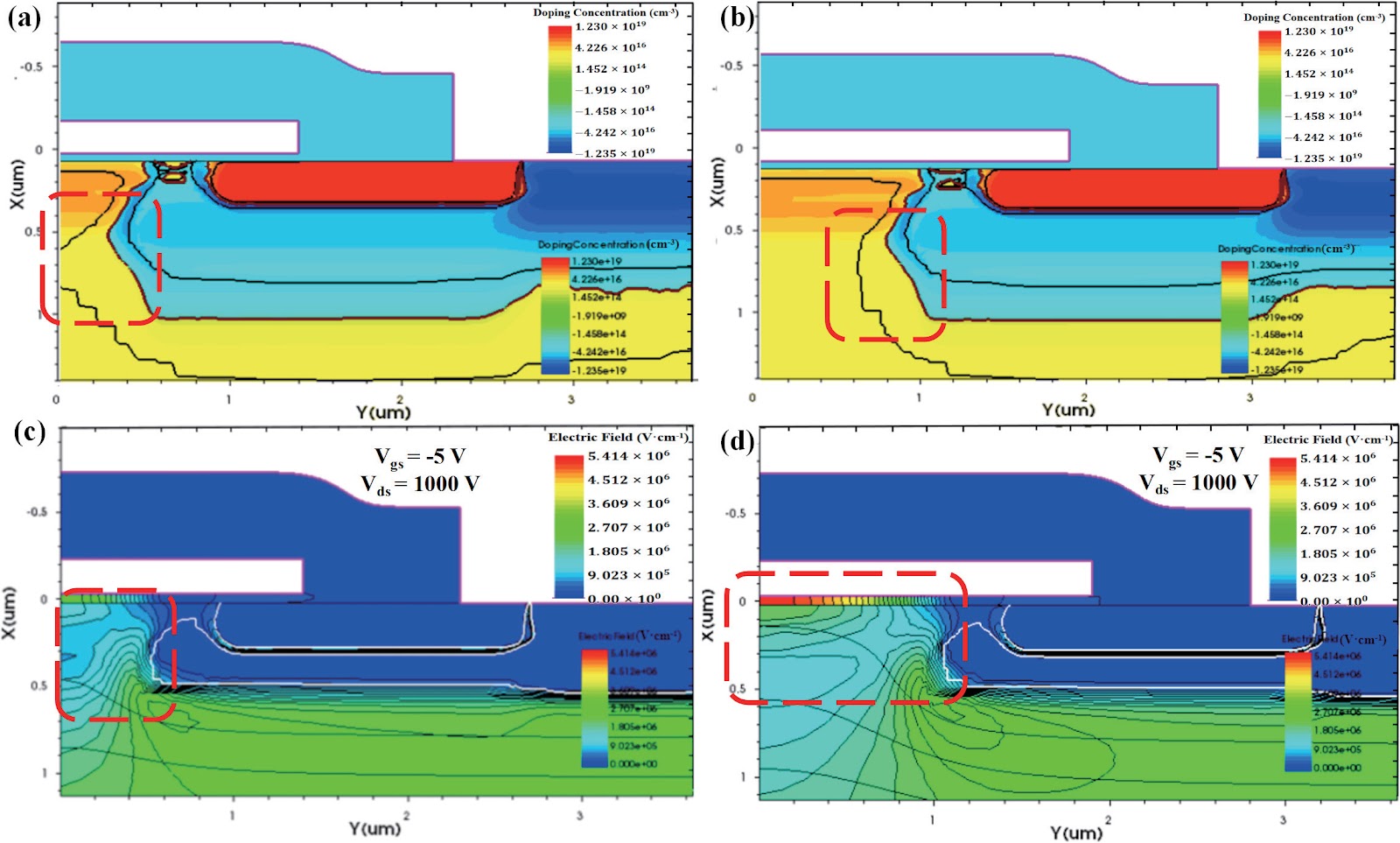
High gate oxide electric field, which can lead to device failure, is a common issue in SiC MOSFETs. To mitigate this issue and ensure high device reliability, an electric field shielding layer (also called depletion layer) in JFET region is always used to reduce the gate oxide electric filed strength (Eox,max). However, there is still a lack of a detection methods to characterize the changes in the depletion layer of the JFET region. In this paper, a type of 1200 V 4H-SiC MOSFET with different JFET widths and cell topologies is designed and fabricated, and an innovative detection method for the depletion layer of JFET region is proposed for the first time. This method is adopted to focus on discussing the influence of the depletion layer formed by different JFET widths on Vg, and the changes in the gate oxide capacitance Cg of hexagonal cells and linear cells during the formation of the JFET depletion layer are studied. Finally, the robustness of different cell topologies and JFET widths is determined by the depletion voltage drift in the high temperature gate reverse bias tests (HTGB−) reliability test.

Effects of cell topology and JFET width on depletion layer of SiC MOSFET
Graphical Abstract
Original ResearchVol. 32, Issue 6 • pp. 100-112DOI: 10.1088/1674-4926/25060021Jan 15, 2025

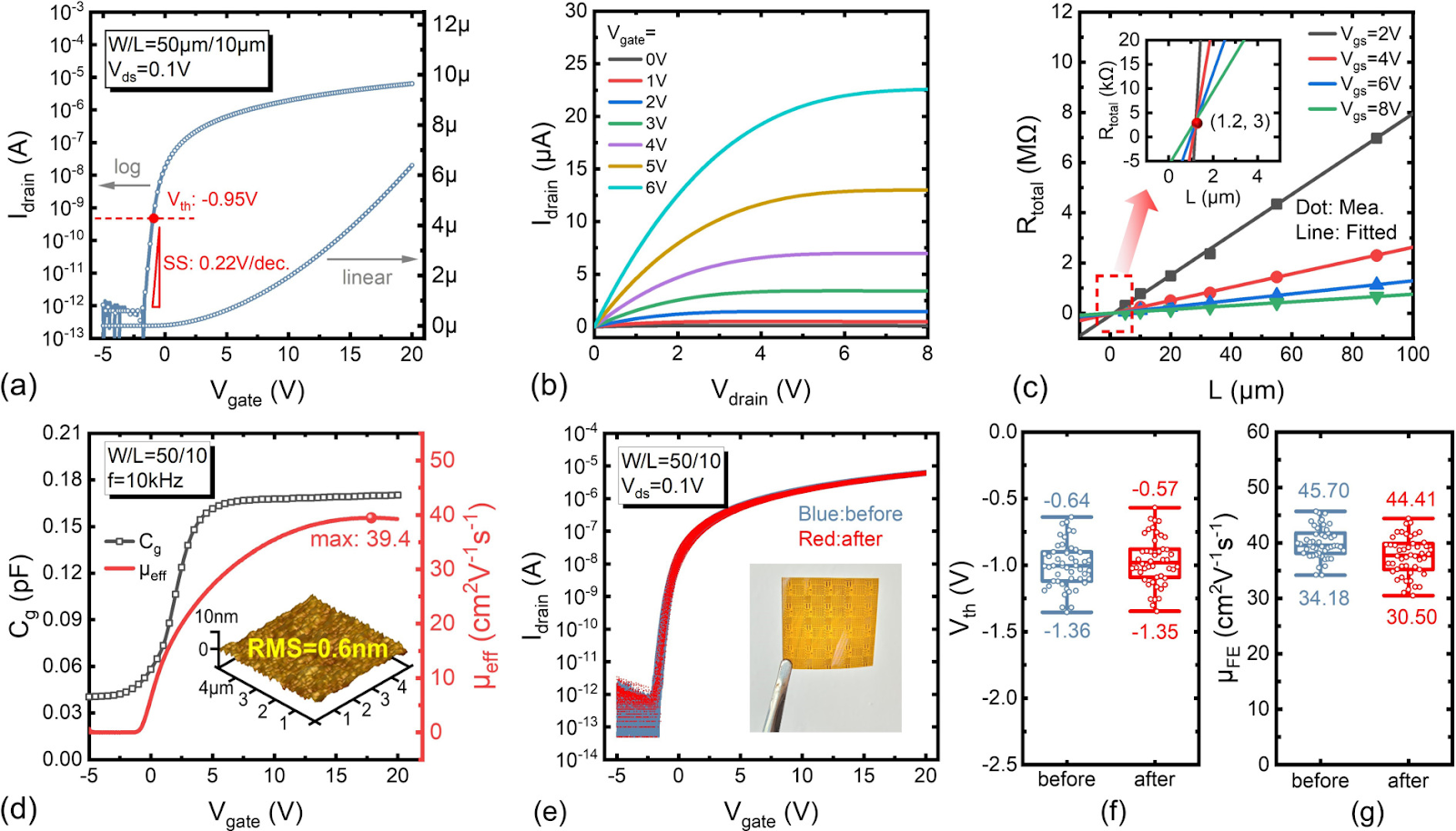
Flexible ITO TFTs with high mobility of 39.1 cm2·V−1·s−1 and excellent uniformity fabricated via mass-production compatible process

Authors: Zuoxu Yu, Yuzhen Zhang, Tingrui Huang, Wenting Xu, Mingming Liu, Di Gui, Kaizhi Sui, Guangan Yang, Weifeng Sun, Runxiao Shi, Wangran Wu

The increasing pursuit of ultra-high resolution displays has driven the demand for thin film transistors (TFTs) with higher mobility, especially on flexible substrates. In this work, we developed indium tin oxide (ITO) TFTs on flexible substrates for the first time and achieved a remarkable average mobility of 39.1 cm2·V−1·s−1, via mass-production compatible processes utilizing SiO2 gate dielectric. Benefiting from the ultra-flat surface and extremely low coefficient of thermal expansion (CTE) of our PI substrate, the ITO TFTs exhibit excellent large-scale uniformity. Additionally, the TFTs generate minor variations of −5.5% and +0.45 V in mobility and threshold voltage under a bending radius of 7 mm, respectively. They stay fully functional even after a dynamic bending test up to 13 000 cycles, observing no obvious degradation in mobility and threshold voltage. The reliable mechanical flexibility and robust bending durability demonstrate their great potential for ultra-high resolution flexible displays in the future.

Flexible ITO TFTs with high mobility of 39.1 cm2·V−1·s−1 and excellent uniformity fabricated via mass-production compatible process
Graphical Abstract
Original ResearchVol. 32, Issue 6 • pp. 100-112DOI: 10.1088/1674-4926/25060031Jan 15, 2025

AlScN: characteristics, micro/nano fabrication and multiple applications

Authors: Shihang Liu, Jinfeng Gao, Jiajie Pan, Lin Li, Hanxiang Jia, Shuangzan Lu, Maowei Zhang, Bo Zhao, Jun Liu

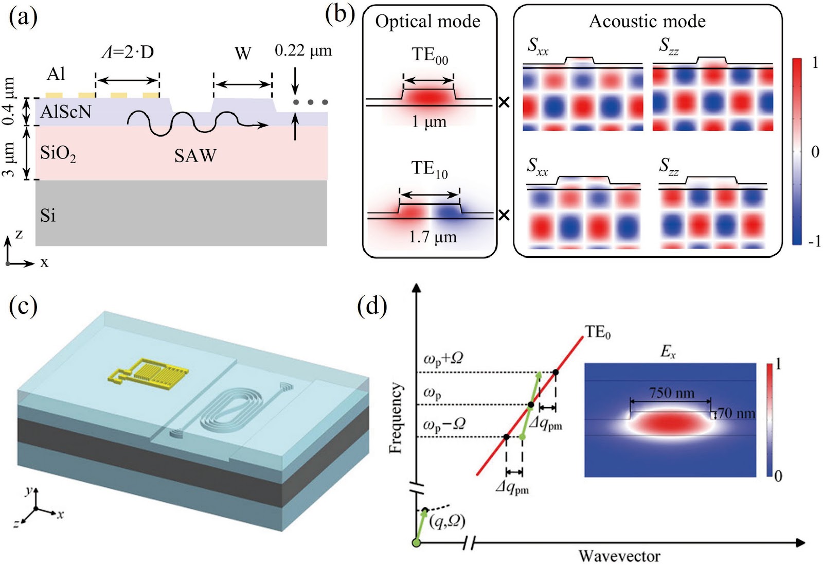
Aluminum scandium nitride (AlScN), an emerging Ⅲ-nitride semiconductor material, has attracted significant attention in recent years due to its exceptional piezoelectric properties, high thermal stability, tunable bandgap, and excellent compatibility with micro/nano fabrication. This paper systematically reviews the crystal structure, fundamental properties, and property modulation mechanisms of AlScN. It also summarizes recent progress in micro/nano fabrication technologies, including deposition, etching, and device integration. Furthermore, the applications of AlScN in diverse fields such as micro-electromechanical systems (MEMS), RF communications, energy conversion, optoelectronics and sensors are discussed. Finally, current challenges and promising future research directions for AlScN are outlined.

AlScN: characteristics, micro/nano fabrication and multiple applications
Graphical Abstract
Original ResearchVol. 32, Issue 6 • pp. 100-112DOI: 10.1088/1674-4926/25060033Jan 15, 2025

Optimizing 55 nm split-gate memory for compute-in-memory: a focus on floating-gate engineering

Authors: Wanyi Ling, Ranran Liu, Kun Ren, Dianyu Qi, Yongyu Wu, Guangji Li, Miao Zhou, Qingshuang Xu, Zhenghui Xia, Xuan Li, Dertsyr Fan, Ichun Chuang, Tzung Wen Cheng, Chenming Tsai, Dawei Gao

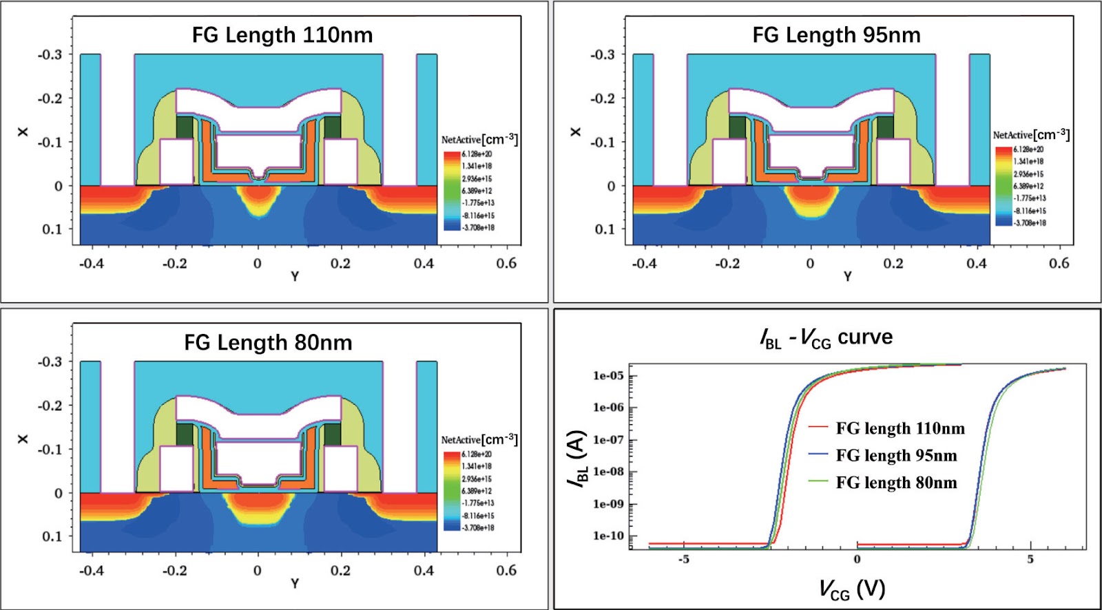
The escalating need for high-performance artificial intelligence (AI) computing intensifies the "memory bottleneck" of the von Neumann architecture, prompting extensive exploration of computation-in-memory (CIM) solutions. This study is centered on the optimization of a high-efficiency, low-power "L"-shaped split-gate floating-gate (FG) memory for CIM applications. Fabricated on a 55 nm CMOS platform, the memory devices were systematically investigated through wafer acceptance test (WAT), Sentaurus™ simulations and comprehensive evaluations with the DNN + NeuroSim Framework V2.0. Among devices with diverse FG lengths, the 95-nm FG variant exhibits outstanding performance: it achieves a 5.35 V memory window, reaches a maximum conductance of 16.7 μS with excellent linearity under the varying voltage and width pulse scheme (VWPS), realizes 32-state multi-level storage, and attains a 92% training accuracy on the CIFAR-10 dataset using the VGG8 neural network.

Optimizing 55 nm split-gate memory for compute-in-memory: a focus on floating-gate engineering
Graphical Abstract
Original ResearchVol. 32, Issue 6 • pp. 100-112DOI: 10.1088/1674-4926/25060032Jan 15, 2025

Optoelectronic synapses based on IGZO/Bi3.25La0.75Ti3O12 heterojunctions for human brain learning mechanism simulation

Authors: Dongping Yang, Hao Chen, Zhenhua Tang, Qijun Sun, Xingui Tang

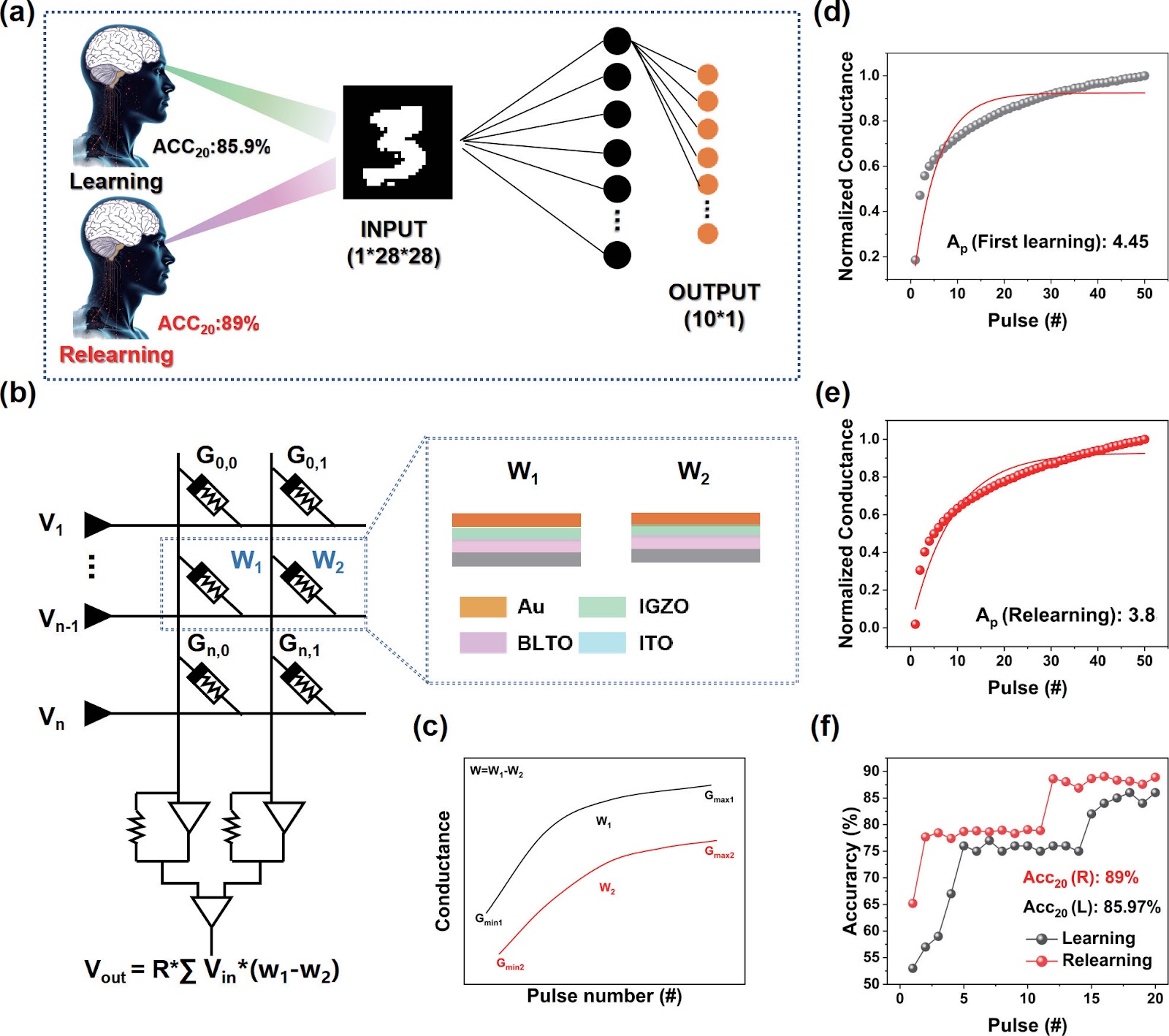
In recent years, optoelectronic synapses have garnered significant attention in the field of neuromorphic computing due to their integration of optical sensing and synaptic functions. In this work, we propose an optoelectronic synapse based on IGZO/Bi3.25La0.75Ti3O12 heterojunction. Under UV light stimulation, this device can simulate a range of synaptic behaviors, including paired-pulse facilitation, spike-intensity-dependent plasticity, spike-number-dependent plasticity, spike-width-dependent plasticity, and the transition from short-term memory to long-term memory. The majority of perceptible information for humans is acquired through the visual system. The 3 × 3 retinal morphology synapse arrays constructed based on plasticity behaviors not only integrates light perception and storage functions but also exhibits adaptive adjustment capabilities to address image blurring caused by object movement. At the same time, in CNN recognition training, the device successfully simulates the learning−relearning mechanism of the human brain. These findings highlight the device’s immense potential for applications in artificial vision systems.

Optoelectronic synapses based on IGZO/Bi3.25La0.75Ti3O12 heterojunctions for human brain learning mechanism simulation
Graphical Abstract
Original ResearchVol. 32, Issue 6 • pp. 100-112DOI: 10.1088/1674-4926/25060014Jan 15, 2025

In situ synthesis and stabilization of perovskite quantum dots in electrospinned fibers

Authors: Alexey Serdobintsev, Vladimir Neplokh, Alexander Koryakin, Ilia Kozhevnikov, Anastasiya Yakubova, Demid Kirilenko, Mariia Saveleva, Sergey Makarov, Ivan Mukhin, Polina Demina

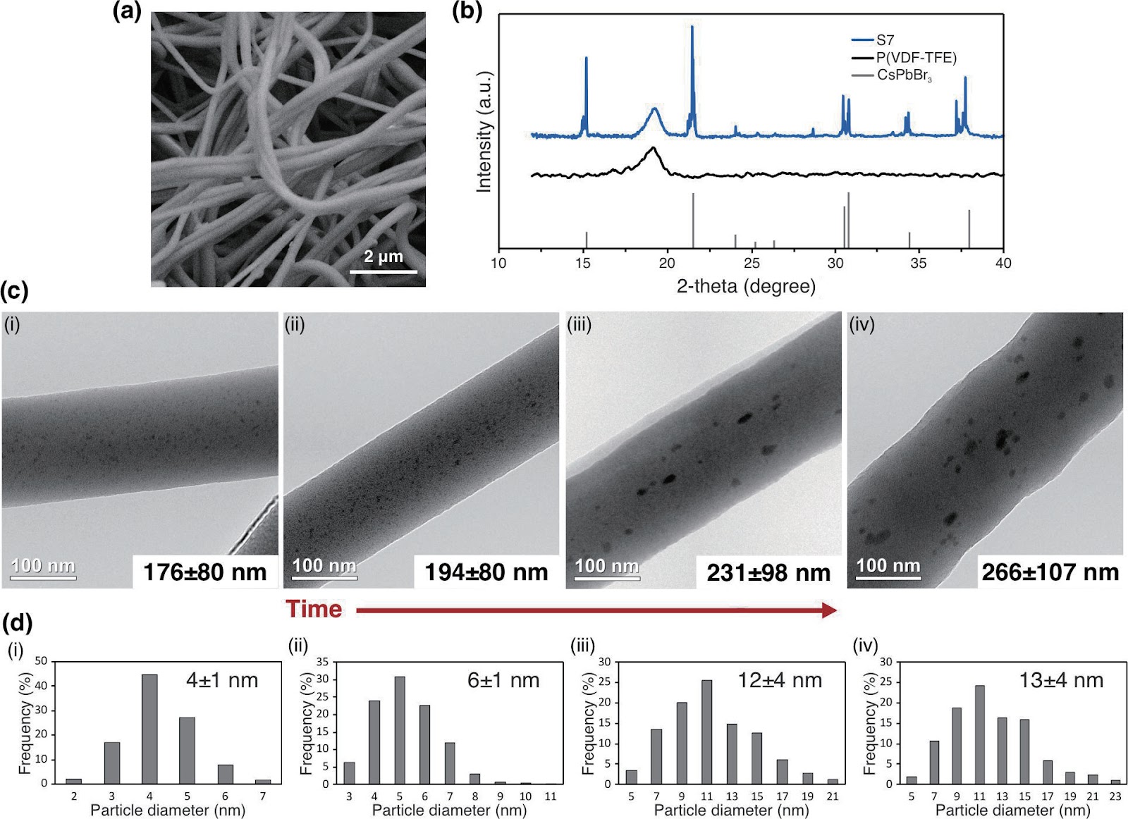
Flexible materials with perovskite quantum dots (PQDs) are widely used in the field of photonics and opto-electronics due to their unique properties. Development of new materials based on these nanoparticles, incorporated into flexible and lightweight nonwoven fabrics, demonstrated high photoconductivity and efficient light energy conversion. In this work, we propose a method for creating a stable luminescent nonwoven material using electrospinning, in which inorganic salt precursors are used without the need for additional stabilizers. Equimolar solutions of cesium and lead (Ⅱ) bromide were mixed with a fluoroplast, resulting in a series of samples. Luminescent materials were obtained containing PQDs with a composition of CsPbBr3, with emission peaks ranging from 507 to 517 nm under 365-nm excitation. We have experimentally established and theoretically confirmed that the peak position is related to the size of the particles formed in the fiber during electrospinning and depends on processing time. Developed materials exhibited stable luminescent properties for up to 2.5 years, making them a promising candidate for the development of new flexible optoelectronic devices based on PQDs.

In situ synthesis and stabilization of perovskite quantum dots in electrospinned fibers
Graphical Abstract
Original ResearchVol. 32, Issue 6 • pp. 100-112DOI: 10.1088/1674-4926/25060004Jan 15, 2025

A deep-junction single-photon detector with field polysilicon gate structure for increased photon detection efficiency and reduced dark count noise

Authors: Zhentao Ni, Dajing Bian, Haoxiang Jiang, Xiaoming Huang, Yue Xu

A high-sensitivity, low-noise single photon avalanche diode (SPAD) detector was presented based on a 180 nm BCD process. The proposed device utilizes a p-implant layer/high-voltage n-well (HVNW) junction to form a deep avalanche multiplication region for near-infrared (NIR) sensitivity enhancement. By optimizing the device size and electric field of the guard ring, the fill factor (FF) is significantly improved, further increasing photon detection efficiency (PDE). To solve the dark noise caused by the increasing active diameter, a field polysilicon gate structure connected to the p+ anode was investigated, effectively suppressing dark count noise by 76.6%. It is experimentally shown that when the active diameter increases from 5 to 10 μm, the FF is significantly improved from 20.7% to 39.1%, and thus the peak PDE also rises from 13.3% to 25.8%. At an excess bias voltage of 5 V, a NIR photon detection probability (PDP) of 6.8% at 905 nm, a dark count rate (DCR) of 2.12 cps/μm2, an afterpulsing probability (AP) of 1.2%, and a timing jitter of 216 ps are achieved, demonstrating excellent single photon detection performance.

A deep-junction single-photon detector with field polysilicon gate structure for increased photon detection efficiency and reduced dark count noise
Graphical Abstract