SinoTechIntel Academic Portal
🏛️ Indexed Academic JournalImpact Factor: 3.8

Journal of Semiconductors (半导体学报 - 中国科学院半导体研究所)

Authoritative peer-reviewed journal in materials science, metallurgy, chemistry and engineering technologies: Journal of Semiconductors (半导体学报 - Viện Bán dẫn CAS)

Total Research Papers: 115
Access: 100% Free Open Access
Browse by Publication Year & VolumeReset All Filters ✕

Published Research PapersFiltered: Year 2026 • Vol. 32 • 2

Showing 17 of 115 peer-reviewed papers with full Graphical Abstracts.

Original ResearchVol. 32, Issue 2 • pp. 100-112DOI: 10.1088/1674-4926/26020002Jan 15, 2026

Mitigating Phosphonic Acid–Perovskite Interfacial Degradation via Molecular Engineering for Ultra-Stable Solar Cells

Authors: LI Xu, GUO Yuxiao, LUO Xin, YAN Haoyuan, XU Bo

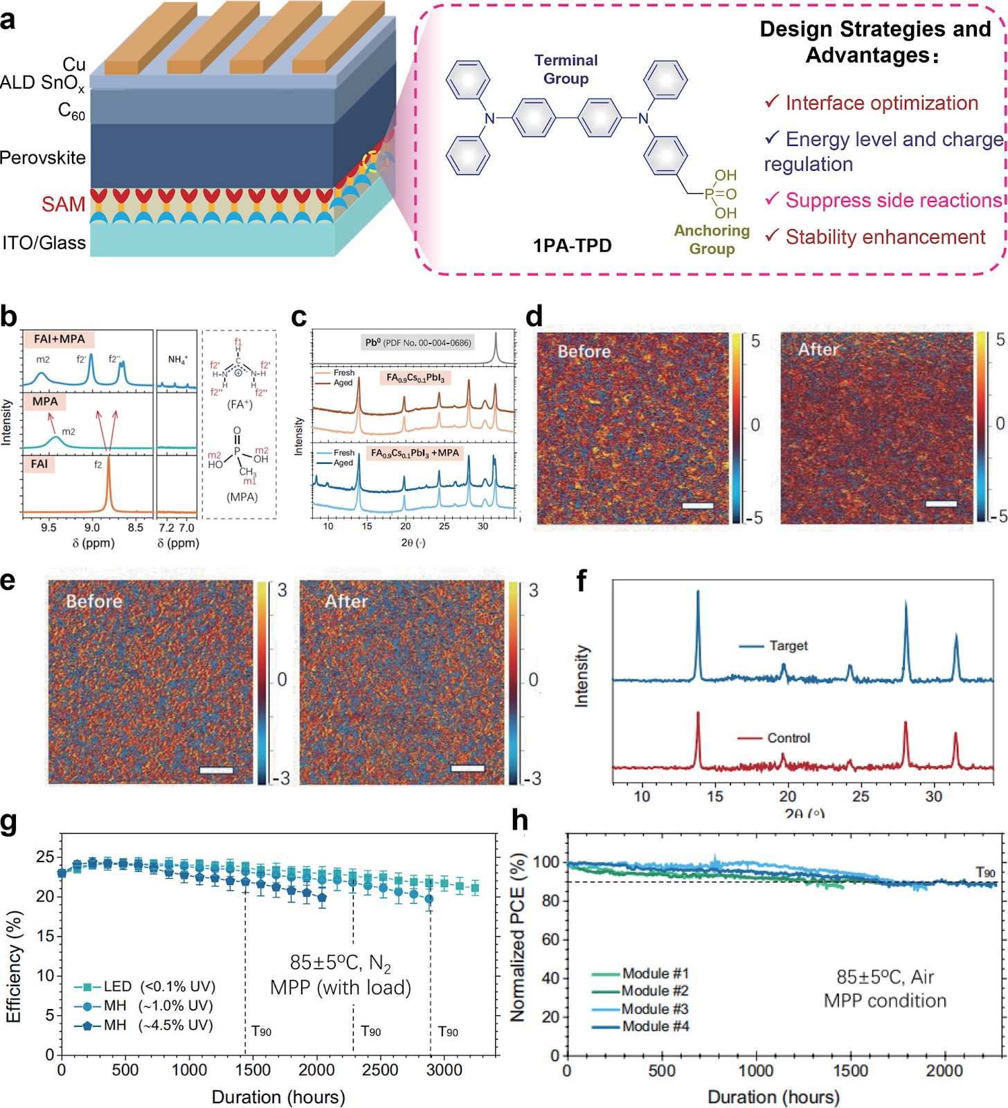
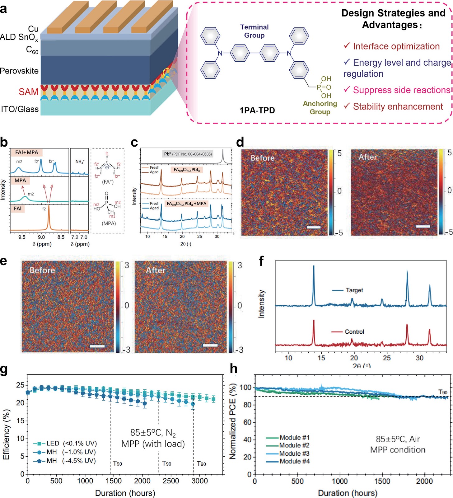
Metal halide perovskite solar cells (PSCs) have emerged as a leading next-generation photovoltaic technology, with certified efficiencies surpassing 27% and approaching the theoretical limit for single-junction devices. However, their commercialization is critically hindered by insufficient long-term operational stability, particularly under harsh conditions such as elevated temperatures (≥85 °C) and full-spectrum illumination. The hole-transport layer (HTL) plays a decisive role in both efficiency and stability, and phosphonic acid-based self-assembled monolayers (PA-SAMs) have become the material of choice for inverted-structure PSCs due to their molecular-scale precision and superior energy-level alignment. Nevertheless, PA-SAMs primarily anchor to ITO surfaces via weak hydrogen bonds, which dissociate under photothermal stress, leading to molecular desorption and migration into the perovskite layer, thereby inducing degradation and performance decline. In a recent breakthrough published in Science (2026), Fei et al. report a transformative molecular engineering strategy that unlocks ultra-stable PSCs. They designed a triphenylamine-based phosphonic acid (1PA-TPD) with robust covalent anchoring to ITO substrates and optimized a mixed SAM system (60 wt% 1PA-TPD + 40 wt% EtCz3EPA), successfully suppressing interfacial reactivity between PA-SAMs and perovskites. This multifunctional strategy integrates strong substrate binding, interfacial reaction inhibition, crystallinity enhancement, and defect passivation, enabling small-area PSCs with a power conversion efficiency (PCE) of 25.0% and a T90 lifetime of nearly 3000 hours, as well as minimodules with >22% PCE and ~2200 hours T90 under harsh photothermal conditions. This work deciphers a previously underappreciated degradation pathway and provides a universal design principle for stable interfacial layers, marking a critical step toward PSC commercialization.
Mitigating Phosphonic Acid–Perovskite Interfacial Degradation via Molecular Engineering for Ultra-Stable Solar Cells
Graphical Abstract
Original ResearchVol. 32, Issue 2 • pp. 100-112DOI: 10.1088/1674-4926/26020050Jan 15, 2026

Crystallization-Sequence Engineering Enables Organic Solar Cell Modules with Efficiencies Exceeding 18%

Authors: Yunhao Cai, Hui Huang

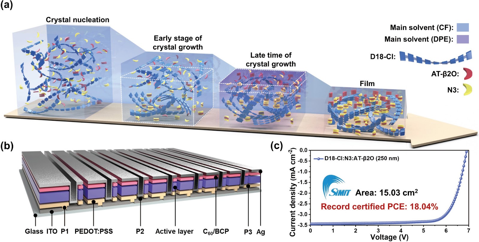
Organic solar cells (OSCs) have emerged as a promising photovoltaic technology due to their mechanical flexibility, low density, and compatibility with solution-based fabrication, enabling applications such as wearable electronics and building-integrated photovoltaics. Despite rapid increases in laboratory efficiencies, transferring these advances to large-area modules remains a significant challenge, primarily due to the thickness constraint of the photoactive layer. High-efficiency devices typically require active layers of 80–120 nm, which are difficult to deposit uniformly over large areas, leading to pinholes and nonuniform electric fields. Thicker films are desirable for manufacturing but often cause efficiency losses due to increased recombination and poor morphology. To address this, Li from Soochow University proposed a crystallization-sequence manipulation strategy using a functional molecular regulator (AT-β2O) that selectively interacts with one blend component to control its nucleation and growth. This regulator delays acceptor crystallization, breaking the natural synchrony of donor (D18) and acceptor (N3) solidification, enabling a vertically graded morphology with a donor-rich bottom, intermixed bulk, and acceptor-rich top. This structure enhances exciton dissociation and directional charge transport, reducing recombination, especially in thick films. Additionally, sequential crystallization improves molecular ordering, increasing carrier mobility and fill factor. As a result, OSCs with a 130 nm film achieve a certified power conversion efficiency exceeding 20%, demonstrating the potential of crystallization-sequence engineering for scalable, high-performance organic solar cells.

Crystallization-Sequence Engineering Enables Organic Solar Cell Modules with Efficiencies Exceeding 18%
Graphical Abstract
Original ResearchVol. 32, Issue 2 • pp. 100-112DOI: 10.1088/1674-4926/26020027Jan 15, 2026

Multi-phase clock generation techniques toward high-frequency and wideband applications

Authors: Junyan Bi, Hao Xu, Na Yan

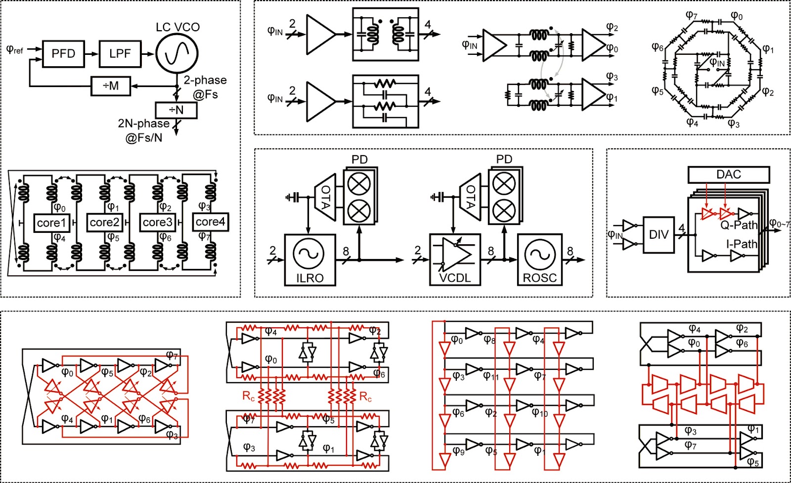
Multi-phase clocks are fundamental components in modern wireline and wireless communication systems, serving as timing and phase references across diverse architectures. As data rates and carrier frequencies scale, the required phase count and operating frequency have increased substantially, pushing conventional clock generation techniques toward their limits. In high-speed wireline transceivers, multi-phase clocks are essential for CDR phase interpolation, time-interleaved ADCs, and advanced PAM-based modulation, imposing stringent requirements on RMS jitter, phase accuracy, and robustness against PVT variations. In wireless and millimeter-wave systems, they are employed for LO generation, quadrature modulation, and beam steering, where phase accuracy often dominates over absolute jitter. Conventional techniques, including PLL-based dividers, multi-core LC oscillators, and passive phase-shifting networks, face scalability challenges at high frequencies, including limited speed, area overhead, narrowband operation, and sensitivity to mismatch. Ring oscillators offer inherent phase scalability and wide tuning range but suffer from poor stability and jitter. Injection-locked ring oscillators (ILROs) enhance stability and phase noise while preserving multi-phase advantages, yet achieving wide locking range and high phase accuracy simultaneously remains challenging. This research highlight reviews these techniques, discusses their limitations, and outlines advanced injection and feedback schemes to overcome these challenges, aiming to guide future developments in high-frequency and wideband multi-phase clock generation.

Multi-phase clock generation techniques toward high-frequency and wideband applications
Graphical Abstract
Original ResearchVol. 32, Issue 2 • pp. 100-112DOI: 10.1088/1674-4926/26020035Jan 15, 2026

Zigzag Domain Walls Unravel the Polarization Switching Puzzle in Wurtzite Ferroelectrics

Authors: Hang Zang, Zhiming Shi, Xiaojuan Sun, Dabing Li

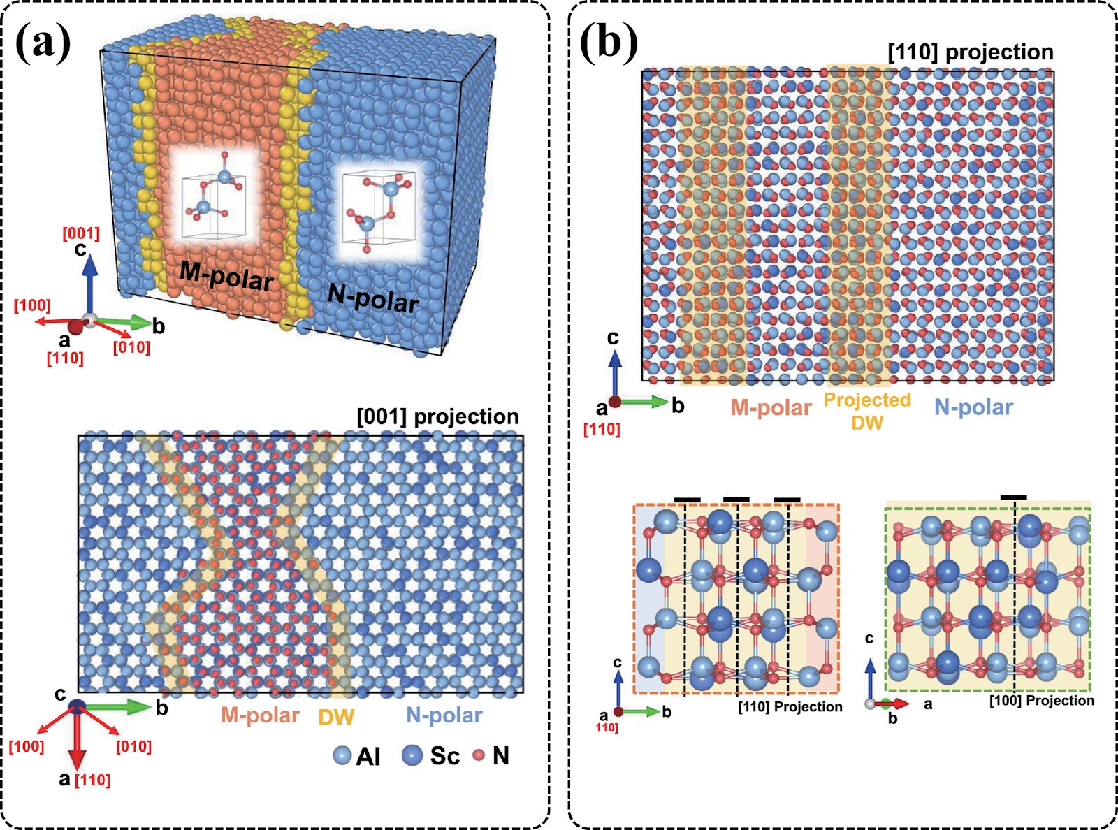
The discovery of robust ferroelectricity in scandium-doped aluminum nitride (Al1−xScxN) has sparked significant interest due to its compatibility with CMOS fabrication, making it a promising candidate for next-generation non-volatile memories and high-frequency devices. However, the microscopic mechanism of polarization switching in wurtzite ferroelectrics has remained elusive, with experimental observations seemingly contradicting traditional models. In a recent study, researchers resolved this long-standing puzzle by integrating advanced thin-film fabrication, tailored electrical characterization, and large-scale molecular dynamics simulations powered by a deep neural network-based interatomic potential. Their findings reveal that the broad 'transitional regions' observed in scanning transmission electron microscopy (STEM) are not a new nonpolar phase but a projection artifact arising from intrinsically three-dimensional zigzag domain walls. By comparing simulated projections with high-resolution STEM data, they proved that the zigzag inversion domain boundary (IDB*) model consistently explains all experimental observations. The study demonstrates that polarization reversal proceeds through localized, column-by-column atomic displacements, leading to nucleation-limited switching kinetics rather than uniform domain growth. Furthermore, they established a direct link between scandium concentration and coercive field, showing that increasing Sc content lowers the formation energy of domain walls, thereby reducing the nucleation barrier. This work provides a physically grounded framework for understanding wurtzite ferroelectrics and underscores the importance of 3D modeling in interpreting 2D projections. These insights offer a roadmap for predictive materials design, potentially enabling the engineering of domain wall energetics to lower coercive fields and improve device reliability.

Zigzag Domain Walls Unravel the Polarization Switching Puzzle in Wurtzite Ferroelectrics
Graphical Abstract
Original ResearchVol. 32, Issue 2 • pp. 100-112DOI: 10.1088/1674-4926/26020045Jan 15, 2026

Crystallization Suppression of Mixed-Halide Intermediates for Perovskite/Cu(In,Ga)Se2 Tandem Solar Cells with Improved Efficiency

Authors: Manya Li, Linjing Jing, Hairen Tan

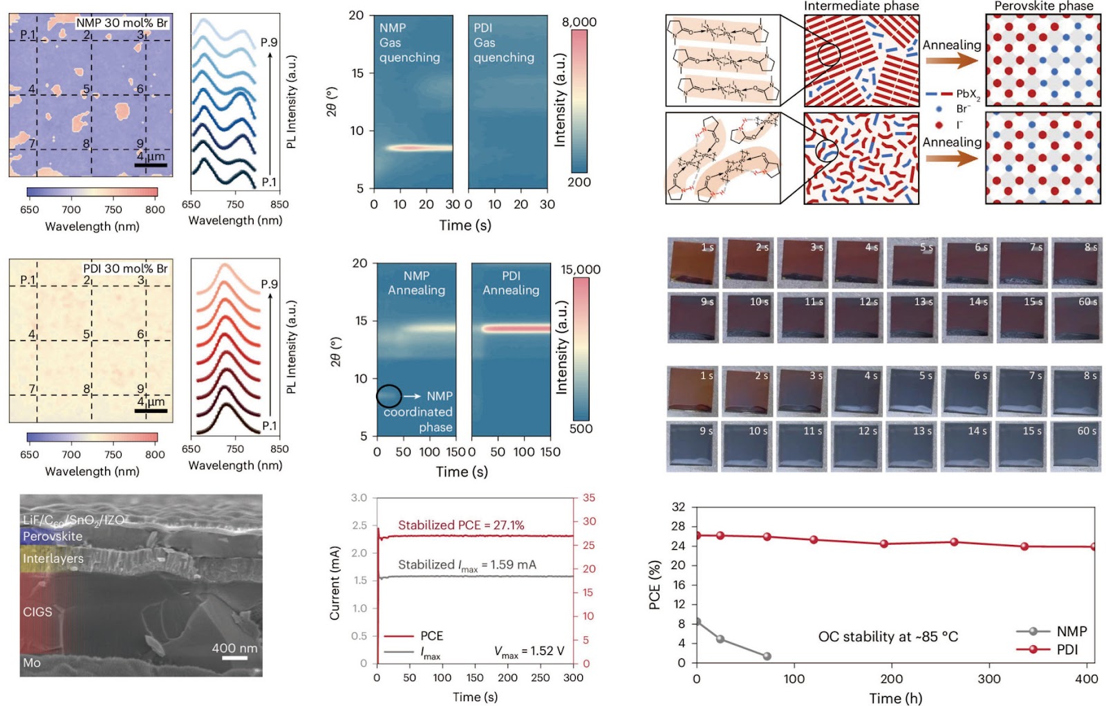
Flexible and lightweight photovoltaics are pivotal for renewable energy applications, and all-thin-film tandem solar cells combining metal-halide perovskites with copper indium gallium selenide (CIGS) offer a synergistic approach to exceed the Shockley-Queisser limit. However, fabricating high-quality wide-bandgap (WBG) perovskite films, especially via scalable blade-coating in ambient air, remains challenging due to uncontrollable crystallization kinetics, phase segregation, and moisture-induced defects. This work addresses these issues by introducing a crystallization suppression strategy that replaces the traditional solvent N-methyl-2-pyrrolidone (NMP) with 2-pyrrolidinone (PDI). In situ grazing-incidence X-ray diffraction (GIXRD) reveals that NMP-based films undergo a crystalline-to-crystalline transition via solvent-coordinated intermediates, leading to residual impurities and incomplete phase transformation. In contrast, PDI, through additional hydrogen bonding, suppresses pre-crystallization and maintains a homogeneous non-crystalline precursor state, enabling a rapid non-crystalline-to-crystalline transition with lower energy barriers. This results in uniform, pinhole-free films with enhanced carrier mobility, longer carrier lifetimes, and reduced trap densities. Single-junction perovskite solar cells fabricated with PDI achieve significantly improved efficiency, demonstrating the effectiveness of this approach for high-performance perovskite/CIGS tandem solar cells.

Crystallization Suppression of Mixed-Halide Intermediates for Perovskite/Cu(In,Ga)Se2 Tandem Solar Cells with Improved Efficiency
Graphical Abstract
Original ResearchVol. 32, Issue 2 • pp. 100-112DOI: 10.1088/1674-4926/26020007Jan 15, 2026

Exciplex-Enabled Fully Stretchable OLEDs Achieve a Record External Quantum Efficiency of 17%

Authors: Meng Wang, Liang Li

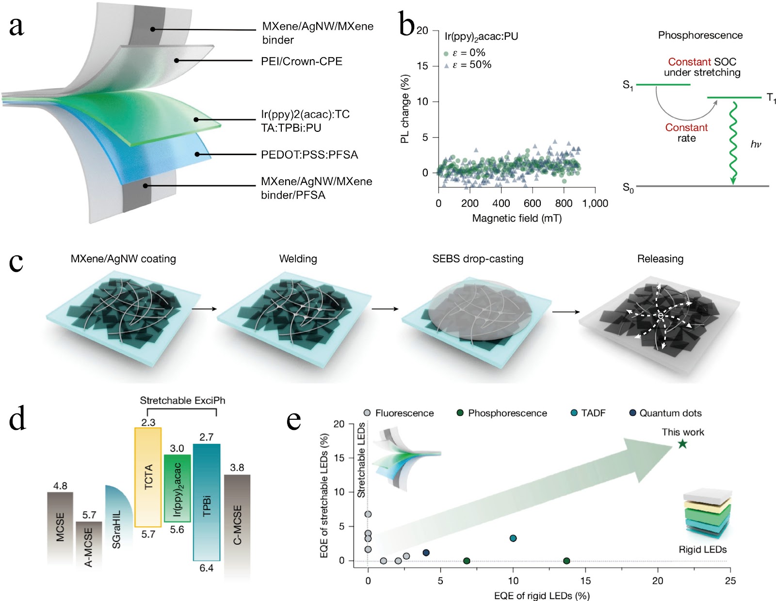
Organic light-emitting diodes (OLEDs) are promising candidates for on-skin applications due to their intrinsic stretchability. However, the external quantum efficiency (EQE) of stretchable OLEDs has long been limited to approximately 10%, stemming from the incorporation of insulating elastomer matrices that hinder exciton energy transfer and charge transport, and from conventional stretchable electrodes with insufficient electrical properties and poor interfacial contact. In a recent breakthrough published in Nature (2026), Gogotsi and Lee reported an exciplex-enabled strategy that overcomes these limitations. By integrating a stretchable exciplex-assisted phosphorescent emitting layer, triplet harvesting is significantly enhanced through an elastomer-tolerant triplet-recycling mechanism. Furthermore, they employ work-function-tunable MXene-contact stretchable electrodes (MCSEs) that provide two-dimensional electrical contact for efficient charge injection. Combining these advances, they achieve an unprecedented EQE of 17% in fully stretchable OLEDs while maintaining excellent mechanical stability. The spin-flip process, which converts non-radiative triplets into radiative singlets, is critical yet challenging in stretchable OLEDs because the necessary spin-orbit coupling (SOC) is sensitive to variations in intermolecular distance under strain. The authors utilize the phosphorescent emitter bis(2-phenylpyridine) (Ir(ppy)2acac), whose heavy-metal iridium center provides strong SOC, enabling nearly complete intersystem crossing and triplet utilization. The study demonstrates that the intrinsic SOC of Ir(ppy)2acac remains stable under 50% tensile strain, preserving both spin-mixing rates and photoluminescence stability. To prevent aggregation-induced quenching and enable efficient energy transfer within a soft matrix, the authors develop a stretchable exciplex-assisted phosphorescent (ExciPh) layer using TCTA and TPBi to form an exciplex cohost, while a thermoplastic polyurethane (PU) elastomer provides mechanical stretchability. This system enables triplet excitons to undergo reverse intersystem crossing (RISC) within a charge-transfer state, followed by long-range Förster resonance energy transfer (FRET) to the phosphorescent dopant. The fabricated OLED demonstrates an EQE of 21.7%, validating the effectiveness of this approach. Beyond the emissive layer, the researchers develop MXene-conductive stretchable electrodes (MCSEs) by integrating a two-dimensional MXene interlayer with silver nanowire (AgNW) networks, achieving a sheet resistance of ~30 Ω/sq with over 85% transmittance at 550 nm and a widely tunable work function (3.79–5.71 eV). They also introduce a stretchable gradient hole injection layer (SGraHIL) that suppresses exciton quenching at the interface while maintaining excellent stretchability. By integrating the SGraHIL, the ExciPh emitting layer, and MCSE electrodes, the authors fabricate fully stretchable OLEDs that achieve an unprecedented EQE of 17%, retaining 83% of initial efficiency after 100 cycles of 20% cyclic strain. This work represents a significant advance in intrinsically stretchable optoelectronics, offering a scalable route toward highly conductive, work-function-tunable contacts and influencing broader fields such as stretchable sensors and soft photonic systems.

Exciplex-Enabled Fully Stretchable OLEDs Achieve a Record External Quantum Efficiency of 17%
Graphical Abstract
Original ResearchVol. 32, Issue 2 • pp. 100-112DOI: 10.1088/1674-4926/26020017Jan 15, 2026

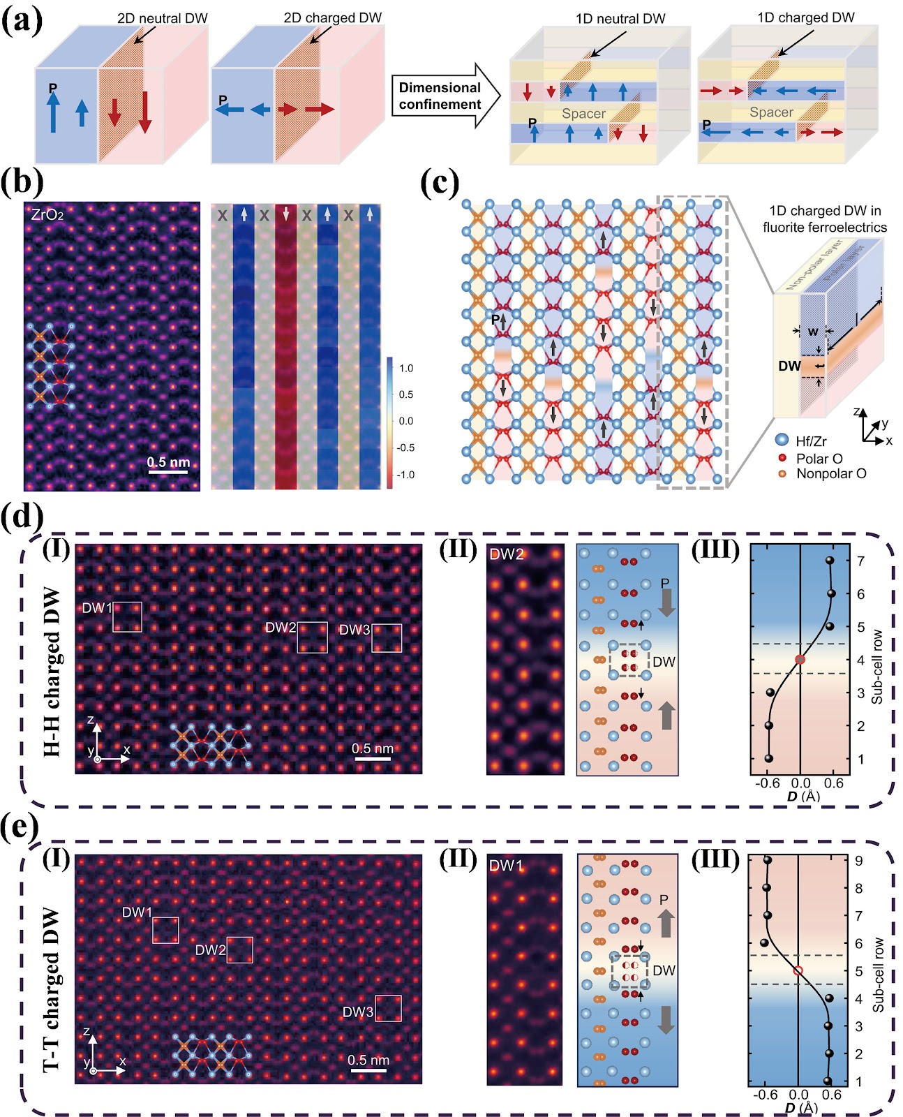
One-dimensional domain walls: A new dimension for ferroelectric nanoelectronics

Authors: Zepeng Li, Wenjing Yue, Yang Li

Topological structures in ferroelectric materials, such as vortices, skyrmions, and merons, have attracted significant attention due to their emergent physical properties distinct from the bulk parent phase. Among these, ferroelectric domain walls (DWs) have long been considered potential active elements for next-generation electronic devices, leading to the paradigm of "domain wall nanoelectronics." However, conventional perovskite ferroelectrics exhibit two-dimensional (2D) domain walls, and charged domain walls (CDWs) suffer from structural broadening due to electronic screening, limiting miniaturization. Recently, a research team led by Chen Ge, Kui-juan Jin, and Qinghua Zhang from the Institute of Physics, Chinese Academy of Sciences, reported the groundbreaking observation of one-dimensional (1D) CDWs in fluorite-structured ferroelectric ZrO2, achieving atomic-scale confinement. Using multislice electron ptychography, they visualized head-to-head and tail-to-tail CDWs with atomic-scale width and thickness (~2.55 Å and ~2.7 Å), equivalent to a single subcell unit. The stability of these atomically thin walls is attributed to a distinct ionic screening mechanism: self-balanced oxygen nonstoichiometry, where H–H walls accumulate excess oxygen ions and T–T walls harbor oxygen vacancies. Furthermore, in situ electric-field experiments demonstrated dynamic manipulation of these 1D structures, revealing a coupling between polarization switching and oxygen ion transport. This discovery breaks the inherent physical limitations of perovskite ferroelectrics and opens new avenues for high-density ferroelectric nanoelectronics.

One-dimensional domain walls: A new dimension for ferroelectric nanoelectronics
Graphical Abstract
Original ResearchVol. 32, Issue 2 • pp. 100-112DOI: 10.1088/1674-4926/26020057Jan 15, 2026

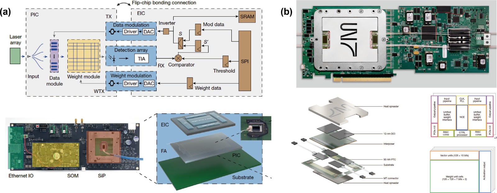
Large-scale integrated photonic accelerators for ultralow-latency and universal AI computing

Authors: Xiangyan Meng, Junshen Li, Kangwei Fei, Yu Wang, Wei Li, Nuannuan Shi, Ming Li

Integrated silicon photonics has emerged as a transformative technology for post-Moore's law computing, offering intrinsic advantages of high bandwidth, ultralow latency, and low energy consumption that far exceed traditional electronic computing architectures. As artificial intelligence (AI) models continue to grow in complexity and scale, the demand for high-speed, energy-efficient computing has spurred intensive research into photonic computing as a promising alternative to electronic accelerators. Matrix multiply-accumulate (MAC) operations, the core of deep learning and combinatorial optimization algorithms, are particularly amenable to photonic implementation, as light enables parallel multiplication and accumulation with minimal data movement. However, the practical application of photonic computing has long been hindered by critical challenges including large-scale integration of photonic components, electro-optical co-packaging, guaranteed computation accuracy of analog photonic systems, and compatibility with mainstream AI models and algorithms. Recently, two groundbreaking studies published back-to-back in Nature have achieved pivotal breakthroughs in addressing these bottlenecks, demonstrating large-scale integrated photonic accelerators with ultralow latency for combinatorial optimization and universal AI computing capabilities for state-of-the-art neural networks. The two works represent the most advanced level of photonic computing hardware implementation to date, validating the feasibility of photonic accelerators as a competitive alternative to electronic AI chips and marking a critical step toward the commercialization of integrated photonic computing technology.

Large-scale integrated photonic accelerators for ultralow-latency and universal AI computing
Graphical Abstract
Original ResearchVol. 32, Issue 2 • pp. 100-112DOI: 10.1088/1674-4926/26020013Jan 15, 2026

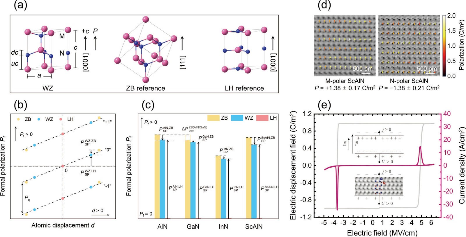
Re-benchmarking Polarization in Wurtzite Nitride Semiconductors

Authors: Ping Wang, Haotian Ye, Rui Wang, Tao Wang, Fang Liu, Zhaoying Chen, Ding Wang, Bo Shen, Xinqiang Wang

Polarization is a defining lever of wurtzite (WZ) III-nitrides. It enables two-dimensional electron and hole gases (2DEG and 2DHG), supports polarization doping, and provides electrostatic control for GaN-based power and radio-frequency (RF) electronics and nitride optoelectronics. Recent advances, especially the emergence of ferroelectric nitrides, have pushed polarization to unprecedented magnitudes and elevated it from a static material constant to an engineering knob. However, the field has long been limited by an uncomfortable reality: the magnitude and orientation of polarization, and its mapping to crystal polarity, have not always been expressed in a self-consistent, experimentally benchmarked language. This mini-review highlights recent progress that rethinks and unifies polarization in wurtzite III-nitride semiconductors. It also discusses how experimental re-benchmarking of giant polarization is reshaping our understanding of nitride polarization and unlocking more predictive polarization engineering for heterostructures and devices.

Re-benchmarking Polarization in Wurtzite Nitride Semiconductors
Graphical Abstract
Original ResearchVol. 32, Issue 2 • pp. 100-112DOI: 10.1088/1674-4926/26020026Jan 15, 2026

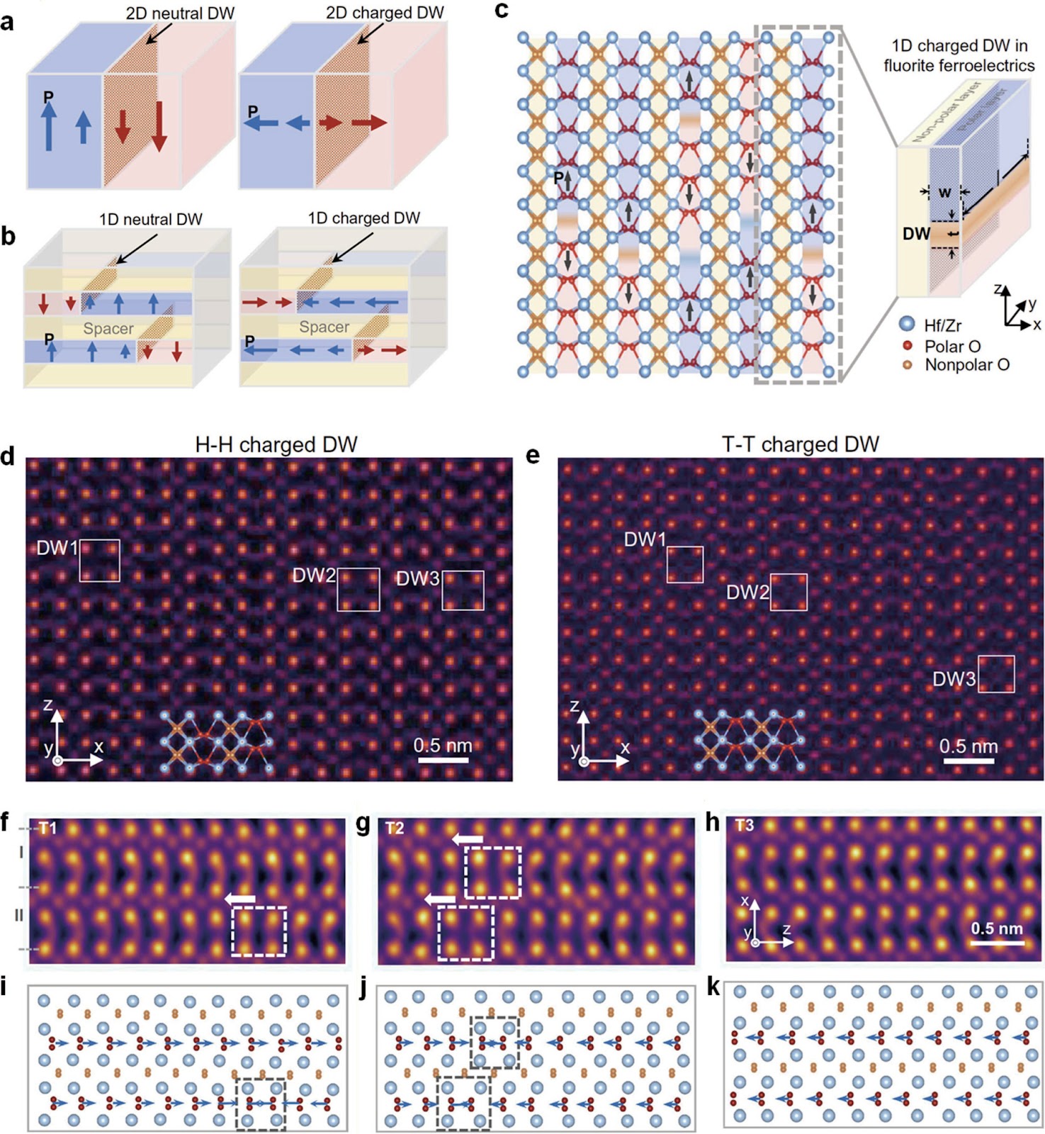
One-dimensional charged domain walls in fluorite ferroelectrics

Authors: Jiajia Chen, Haoji Qian, Xiaoxi Li, Yan Liu, Chengji Jin, Genquan Han

Ferroelectric domain walls are conventionally regarded as two-dimensional (2D) interfacial objects that separate regions of different polarization within a crystal. This picture has guided decades of research into polarization switching, domain evolution, and ferroic functionality. In most ferroelectrics, electrostatic considerations strongly favor head-to-tail (H–T) polarization configurations, which minimize bound charge and reduce electrostatic energy. By contrast, charged domain walls (CDWs) carry positive or negative bound polarization charge and form where polarization vectors arrange head-to-head (H–H) or tail-to-tail (T–T), generally considered energetically unfavorable. When such charged walls do occur, they are typically stabilized only as extended 2D structures through a combination of electronic screening, defect accumulation, and lattice relaxation. Despite these energetic constraints, CDWs have attracted growing interest over the past decade because of their emergent functional properties, including enhanced electrical conductivity, strong electromechanical coupling, and reconfigurable electronic behavior localized at charged walls, motivating the broader concept of domain-wall nanoelectronics. Nevertheless, ferroelectric domain walls have almost universally been treated as quasi-2D objects. Further reduction of their dimensionality has long been assumed to be impractical, particularly for charged walls, because confining bound polarization charge to lower dimensions would dramatically increase electrostatic energy. Against this backdrop, Zhong et al. reported the direct observation of one-dimensional (1D) CDWs confined within individual polar layers of ferroelectric ZrO2 (Science (2026)). Using atomic-resolution electron microscopy combined with in situ electric-field manipulation, they demonstrated that both H–H and T–T CDWs can exist as atomic-scale line defects rather than extended 2D interfaces, with their bound polarization charge stabilized through a self-balancing oxygen compensation mechanism. The discovery represents an extreme limit of ferroelectric domain-wall confinement and introduces a fundamentally new class of polar topological objects that occupy an intermediate conceptual regime between conventional domain walls and line defects.

One-dimensional charged domain walls in fluorite ferroelectrics
Graphical Abstract
Original ResearchVol. 32, Issue 2 • pp. 100-112DOI: 10.1088/1674-4926/26020023Jan 15, 2026

Three-Panchromatic Organic Self-Adaptive Transistors for In-Pixel Color Correction

Authors: Yuan Tan, Wei Deng, Xiujuan Zhang, Jiansheng Jie

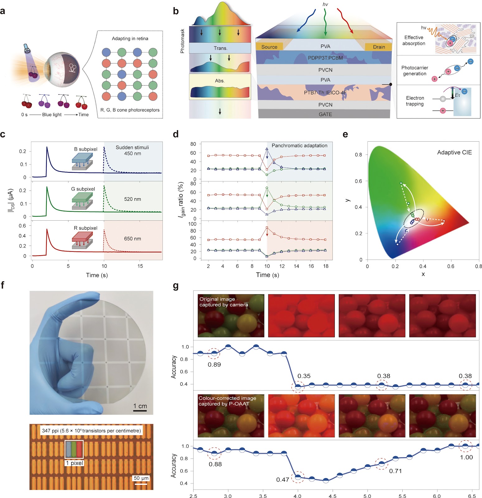
Machine vision systems face a fundamental challenge of illumination-dependent color shift, which conventional post-capture white-balance correction methods address at the cost of computational overhead and latency. Inspired by the human retina's chromatic adaptation, we propose a three-panchromatic organic self-adaptive transistor (OAAT) that embeds color correction directly at the pixel level. The device integrates a dual-layer complementary bulk heterojunction (BHJ) into an organic transistor architecture: a PTB7-Th:IEICO-4F blend serves as the adaptive photoresponse layer with broad-spectrum absorption and wavelength-insensitive trap activation energy that decreases with light intensity, while a PDPP3T:PCBM layer provides spectrally compensatory sensing. This design enables rapid, stable, and intensity-dependent photoadaptation, with an active adaptation index exceeding 150 for red, green, and blue stimuli. Under spectrally biased illumination, the device's responses follow von Kries coefficients and converge to a white-like chromatic state within seconds, demonstrating true chromatic adaptation. Wafer-scale fabrication achieved a 96.1% yield across 256 transistors, with pixel density of 347 ppi and over one million pixels integrated on a four-inch sapphire substrate. In a hybrid artificial visual system combining the OAAT array with a lightweight CNN, in-sensor correction restored classification accuracy for 'frog' in CIFAR-10 from 59.1% to 96.3% under blue-light interference, and outperformed conventional RGB cameras in real-world non-uniform lighting. This work presents a scalable, hardware-based solution for in-pixel color correction, promising for energy-efficient and real-time machine vision.

Three-Panchromatic Organic Self-Adaptive Transistors for In-Pixel Color Correction
Graphical Abstract
Original ResearchVol. 32, Issue 2 • pp. 100-112DOI: 10.1088/1674-4926/26020002Jan 15, 2026

Mitigating phosphonic acid-perovskite interfacial degradation via molecular engineering for ultra-stable solar cells

Authors: LI Xu, GUO Yuxiao, LUO Xin, YAN Haoyuan, XU Bo

Metal halide perovskite solar cells (PSCs) are revolutionizing next-generation photovoltaics by combining high efficiency with low-cost solution processing and flexible compatibility. Certified efficiencies now surpass 27%, nearing the theoretical limit for single-junction cells and highlighting their strong potential for commercialization. In contrast to traditional silicon cells, which require high-temperature processing and rigid substrates, PSCs can be fabricated near room temperature using earth-abundant materials, significantly lowering energy consumption and production costs. However, their commercialization is hindered by a fundamental challenge: insufficient long-term operational stability. PSCs must endure harsh real-world conditions, including elevated temperatures (≥85 °C) and full-spectrum illumination. Meeting the International Electrotechnical Commission (IEC) standard of ≥25 years of service life remains an unresolved critical hurdle for SAM-based PSCs. The hole-transport layer (HTL) plays a decisive role in both the efficiency and long-term stability of PSCs, responsible for efficiently extracting photogenerated holes from the perovskite layer to the transparent conductive oxide electrode. Inadequate extraction leads to severe interfacial charge recombination and significant efficiency losses. Among various HTL materials, phosphonic acid-based self-assembled monolayers (PA-SAMs) have become the material of choice for inverted-structure PSCs, owing to their molecular-scale precision, ultrathin film formation, and superior energy-level alignment—properties that effectively suppress non-radiative recombination and enhance initial device performance. Nevertheless, their practical application is severely limited by an inherent flaw: PA-SAMs primarily anchor to ITO surfaces via weak hydrogen bonds, which dissociate under photothermal stress. This triggers molecular desorption and migration into the perovskite layer, inducing degradation and eventual performance decline. To tackle this persistent issue, Fei et al. report a transformative molecular engineering strategy that unlocks ultra-stable PSCs (Science 2026, https://doi.org/10.1126/science.adz7969). The team designed a triphenylamine-based phosphonic acid (1PA-TPD) with robust covalent anchoring to ITO substrates and optimized a mixed SAM system (60 wt% 1PA-TPD + 40 wt% EtCz3EPA), successfully suppressing interfacial reactivity between PA-SAMs and perovskites. This multifunctional strategy integrates strong substrate binding, interfacial reaction inhibition, crystallinity enhancement, and defect passivation.

Mitigating phosphonic acid-perovskite interfacial degradation via molecular engineering for ultra-stable solar cells
Graphical Abstract
Original ResearchVol. 32, Issue 2 • pp. 100-112DOI: 10.1088/1674-4926/26020058Jan 15, 2026

A Transferable Route to Two-Dimensional Gate-All-Around Electronics

Authors: Jian Wang, Ruiqin Wu, Jianfeng Jiang

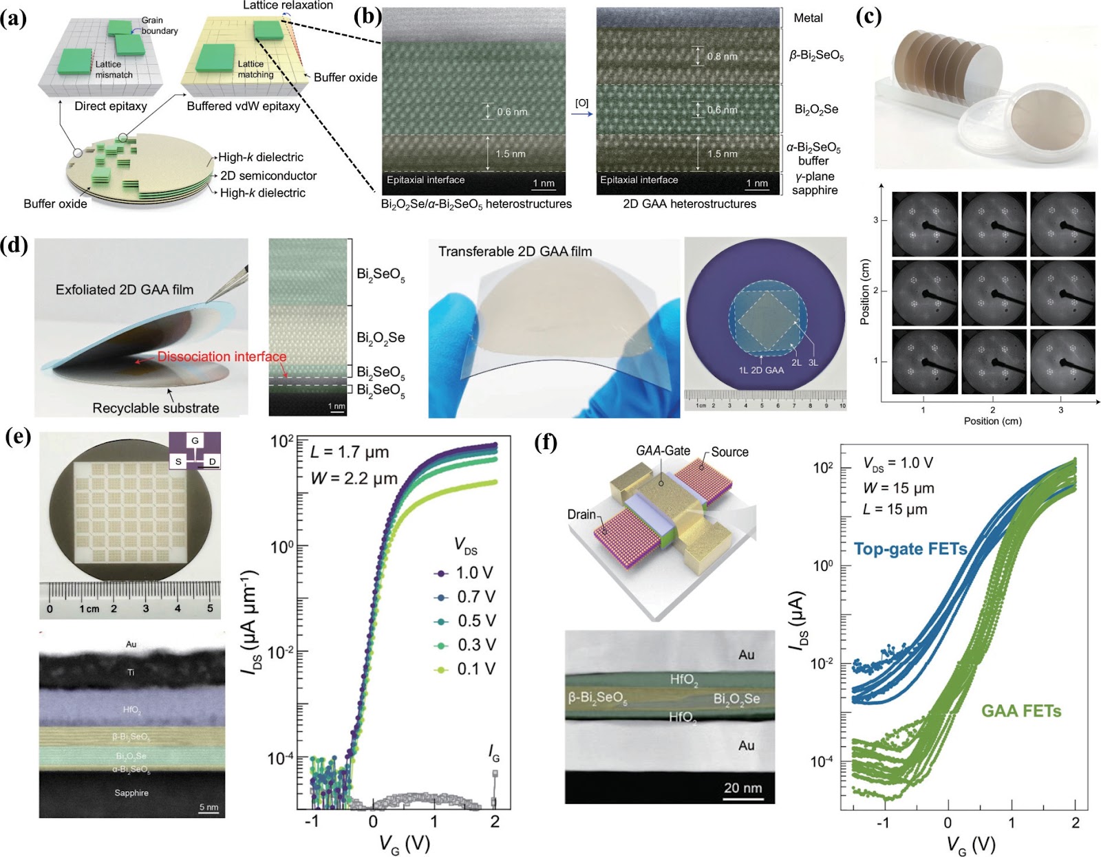
The relentless drive for miniaturization in microelectronics, guided by Moore's Law, is approaching a critical inflection point. Silicon-based transistors are confronting fundamental physical limits at the atomic scale, where issues of power leakage and degraded electrostatic control become increasingly severe. To sustain performance scaling, the semiconductor industry is transitioning to gate-all-around (GAA) nanosheet architectures for sub-2-nanometer technology nodes. However, integrating atomically thin two-dimensional (2D) semiconductors as channel materials within GAA structures offers a revolutionary path, promising superior electrostatic control and lower power consumption. The grand challenge has been the absence of a scalable, industry-compatible method to synthesize high-quality, uniform 2D semiconductor channels seamlessly encapsulated by high-k gate dielectrics in a GAA configuration. A groundbreaking study by Peng et al. reports the wafer-scale, uniform synthesis of single-crystalline 2D high-k dielectric/semiconductor/high-k dielectric GAA heterostructures via an innovative buffered van der Waals epitaxy technique. The core innovation lies in pre-depositing a high-k van der Waals buffer oxide (α-Bi2SeO5) on an r-plane sapphire substrate, which mitigates lattice mismatch and enables epitaxial growth of uniform Bi2O2Se films. Controlled oxidation transforms the top layer into β-Bi2SeO5, forming a sandwich-like GAA heterostructure with atomically sharp interfaces. The intrinsic transferability of these stacks allows clean exfoliation and transfer onto arbitrary substrates, leaving the sapphire wafer reusable. Field-effect transistors fabricated from these heterostructures exhibit outstanding electrical characteristics: on/off ratios exceeding 10^6 and carrier mobility up to 227 cm²·V⁻¹·s⁻¹. True GAAFETs using both top and bottom gates show improved subthreshold swing and higher on/off ratios, demonstrating superior gate controllability. This work represents a foundational platform technology addressing critical integration challenges for 2D semiconductors, bridging laboratory exploration and foundry-level manufacturing, and enabling monolithic 3D integration for future electronics.

A Transferable Route to Two-Dimensional Gate-All-Around Electronics
Graphical Abstract
Original ResearchVol. 32, Issue 2 • pp. 100-112DOI: 10.1088/1674-4926/26020030Jan 15, 2026

Stabilizing Perovskite Fabrication in Ambient Air

Authors: GONG Ruihao, YAN Buyi, LAN Dongchen

Perovskite-based solar cells have advanced rapidly due to their high efficiency potential, low-cost processing, and flexible fabrication routes. While silicon solar cells remain the dominant commercial technology, combining perovskites with silicon in tandem architectures offers a clear pathway to exceed the efficiency limits of single-junction devices. By pairing perovskite's tunable absorption with silicon's proven performance, perovskite–silicon tandem solar cells open new opportunities for high-efficiency photovoltaics. Yet translating these advances from laboratory demonstrations to scalable manufacturing remains a major challenge. A central obstacle lies in fabricating high-quality perovskite films under ambient conditions. Moisture in air directly interferes with perovskite crystallization, leading to disordered crystal growth, surface degradation, and the accumulation of non-ideal secondary phases. Although thermal annealing is often used to improve crystallinity, the combined effects of heat and humidity can instead accelerate irreversible degradation when processing in air. Together, these factors make crystallization control under ambient conditions particularly difficult, underscoring the need for new strategies that can stabilize film formation without relying on tightly controlled environments. Previous studies have explored several approaches to optimize perovskite film fabrication in ambient air, such as solvent engineering and longitudinal homogeneous intermediates in hybrid sequential deposition, as well as techniques like the P1.5 process that introduce a diffusion barrier layer. However, challenges persist, particularly in achieving the same performance as films fabricated in controlled environments. Now, writing in Joule, Tan et al. tackle this challenge with a novel approach that intervenes in the wet-film stage to stabilize the crystallization process. Instead of relying on environmental controls to eliminate moisture, the authors introduce an additive, n-butylammonium thiocyanate (nBASCN), to regulate crystallization dynamics. Implemented as part of the hybrid sequential deposition process, this wet-film intervention modifies the crystallization pathway, preventing premature nucleation and promoting uniform growth. The key innovation lies in the use of nBASCN to decouple diffusion from crystallization, enabling uniform crystallization and improving film quality under ambient conditions. This intervention not only improves film quality but also enhances device performance, with nBASCN-treated devices achieving higher power conversion efficiency (PCE) compared to untreated controls. Beyond improving single-junction perovskite solar cells, this approach is also effective for tandem solar cells, demonstrating the strategy's applicability to more complex multi-junction devices. This marks a crucial step toward achieving scalable, high-efficiency tandem solar cells.

Stabilizing Perovskite Fabrication in Ambient Air
Graphical Abstract
Original ResearchVol. 32, Issue 2 • pp. 100-112DOI: 10.1088/1674-4926/26020044Jan 15, 2026

Improved Solvent Systems for the Commercialization of Perovskite Photovoltaic Modules

Authors: Zhaoyang Chu, Xiaotian Hu, Yiwang Chen

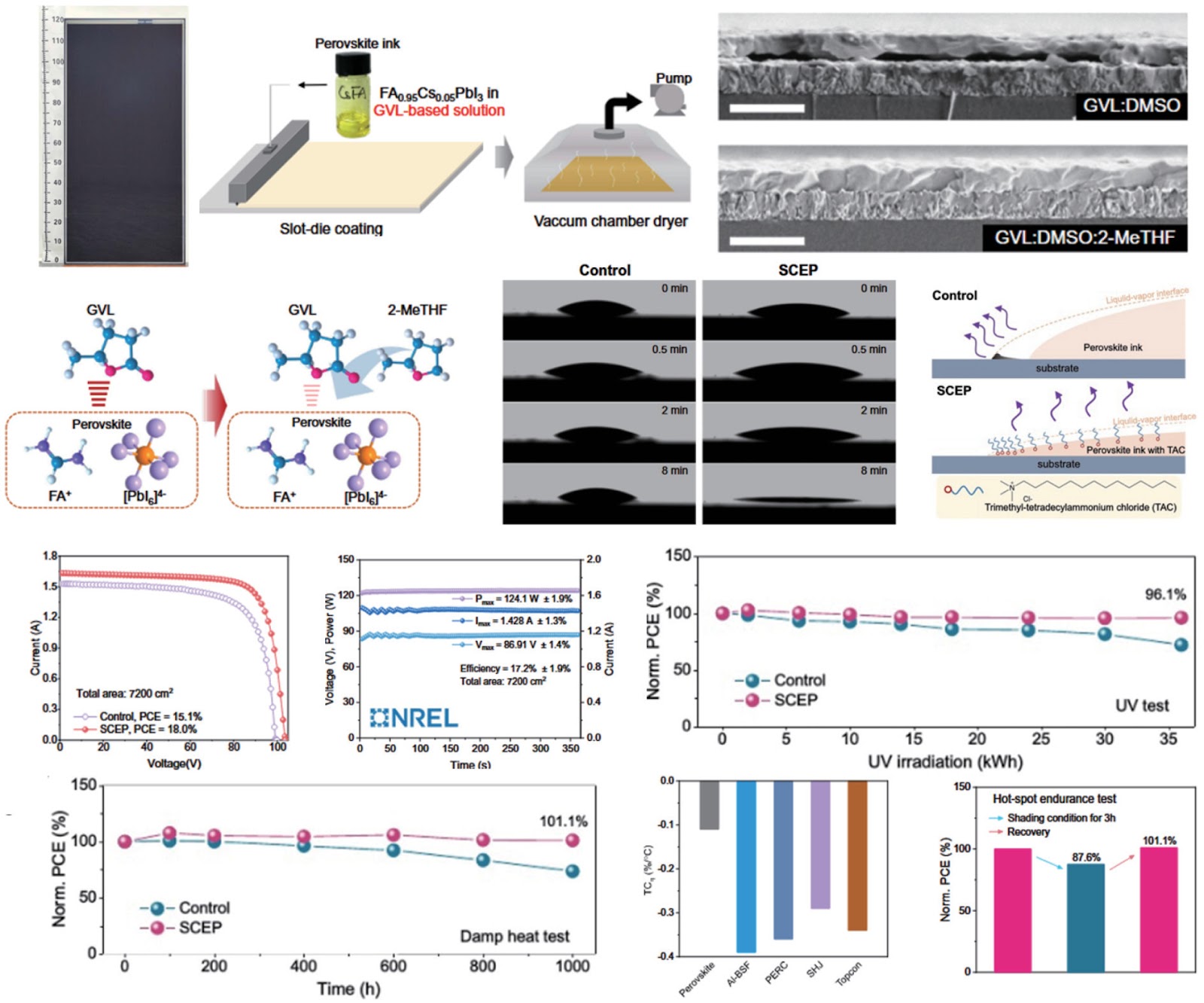
Perovskite solar cells (PSCs) are widely recognized as a transformative technology for next-generation photovoltaics, given their exceptional promise for achieving high power conversion efficiencies (PCE), utilizing low-cost raw materials, and enabling versatile fabrication routes. However, commercialization efforts continue to face considerable obstacles, such as the dependence on toxic solvents, inadequate uniformity in large-area film deposition, and limited operational durability. Conventional perovskite inks commonly rely on highly toxic, high-boiling-point aprotic polar solvents, including N,N-dimethylformamide (DMF) and N-methyl-2-pyrrolidone (NMP). These solvents present serious environmental and health hazards while also impeding processing speeds and perovskite film quality in scalable high-throughput manufacturing, such as roll-to-roll slot-die coating, owing to their slow evaporation kinetics. Furthermore, residual solvent and heterogeneous crystallization tend to introduce a high density of defects in perovskite films, which undermines the long-term stability and reliability of the resulting perovskite photovoltaic modules (PPM) and hinders compliance with the rigorous standards required for commercial deployment. Thus, the establishment of an eco-friendly and efficient solvent system is essential for enabling the widespread adoption of perovskite technology in the mainstream photovoltaic market. In this context, Wang et al. devised an eco-friendly ink formulation utilizing green solvents (γ-valerolactone (GVL), dimethylsulfoxide (DMSO) and 2-methyltetrahydrofuran (2-MeTHF)), and integrated it with a solvent-constrained edge-protection (SCEP) strategy. This approach enhanced the edge quality of perovskite films and lowered defect density under ambient conditions, thereby enabling the scalable production of high-performance PPM (Science, 2025, 390, 1021-1028). These approaches enabled the production of 7200-square-centimeter PPM that achieved a certified stabilized efficiency of 17.2% by NREL. In addition, the scalable module passed all IEC 61215 reliability standards as certified by TÜV Rheinland. This work has realized a PPM with a certified stabilized efficiency of 17.2% over an area of 7200 cm2. The adoption of green solvents not only addresses environmental and regulatory concerns, but also owing to their lower boiling point and the optimized process flow, which reduces energy consumption during production. Combined with slot-die coating technology, which is well-suited for large-scale roll-to-roll manufacturing, the proposed solution demonstrates considerable potential for achieving highly competitive levelized cost of electricity in the future, thereby accelerating the commercialization of perovskite photovoltaics.

Improved Solvent Systems for the Commercialization of Perovskite Photovoltaic Modules
Graphical Abstract
Original ResearchVol. 32, Issue 2 • pp. 100-112DOI: 10.1088/1674-4926/26020015Jan 15, 2026

Ultrathin van der Waals Ferroelectric Oxides for Scalable Low-Power Memory

Authors: Xiaokun Qin, Bowen Zhong, Zheng Lou, Lili Wang

The continuous scaling of ferroelectric memories to below 5 nm has exacerbated challenges such as depolarization fields, interfacial charge trapping, and structural non-uniformity, which critically bottleneck the performance and consistency of ferroelectric field-effect transistors (FeFETs). Although van der Waals ferroelectrics offer a promising route to overcome interface-related issues and critical-thickness limits, the lack of wafer-scale, CMOS-compatible ultrathin ferroelectric materials with robust polarization and high dielectric constants has hindered practical deployment. In a recent study published in Science (2026), Peng and colleagues report a wafer-scale, ultrathin van der Waals ferroelectric oxide platform that addresses these challenges via a controlled oxidation strategy, transforming a two-dimensional semiconductor precursor into a layered ferroelectric oxide with atomically smooth and chemically coherent interfaces. This native-oxide approach enables robust and switchable polarization down to the monolayer limit, as demonstrated by domain writing and erasing. The platform supports monolithic integration of FeFET arrays over centimetre-scale areas, exhibiting consistent hysteresis windows and switching thresholds across hundreds of devices, with narrow distributions of on/off ratios and threshold voltages. Furthermore, the programmable coupling between ferroelectric polarization and semiconductor channels enables multi-level threshold voltage programmability and stable switching between logic states, positioning these devices as reconfigurable building blocks for low-power memory and computing-in-memory architectures. This work bridges the gap between atomic-scale ferroelectric physics and manufacturable device architectures, offering a scalable path for next-generation non-volatile memory.

Ultrathin van der Waals Ferroelectric Oxides for Scalable Low-Power Memory
Graphical Abstract
Original ResearchVol. 32, Issue 2 • pp. 100-112DOI: 10.1088/1674-4926/26020003Jan 15, 2026

Material Platforms for Solid-State Single-Photon Sources: Wide Bandgap Semiconductors

Authors: MENG Junhua, SHI Yiming, ZHANG Xingwang

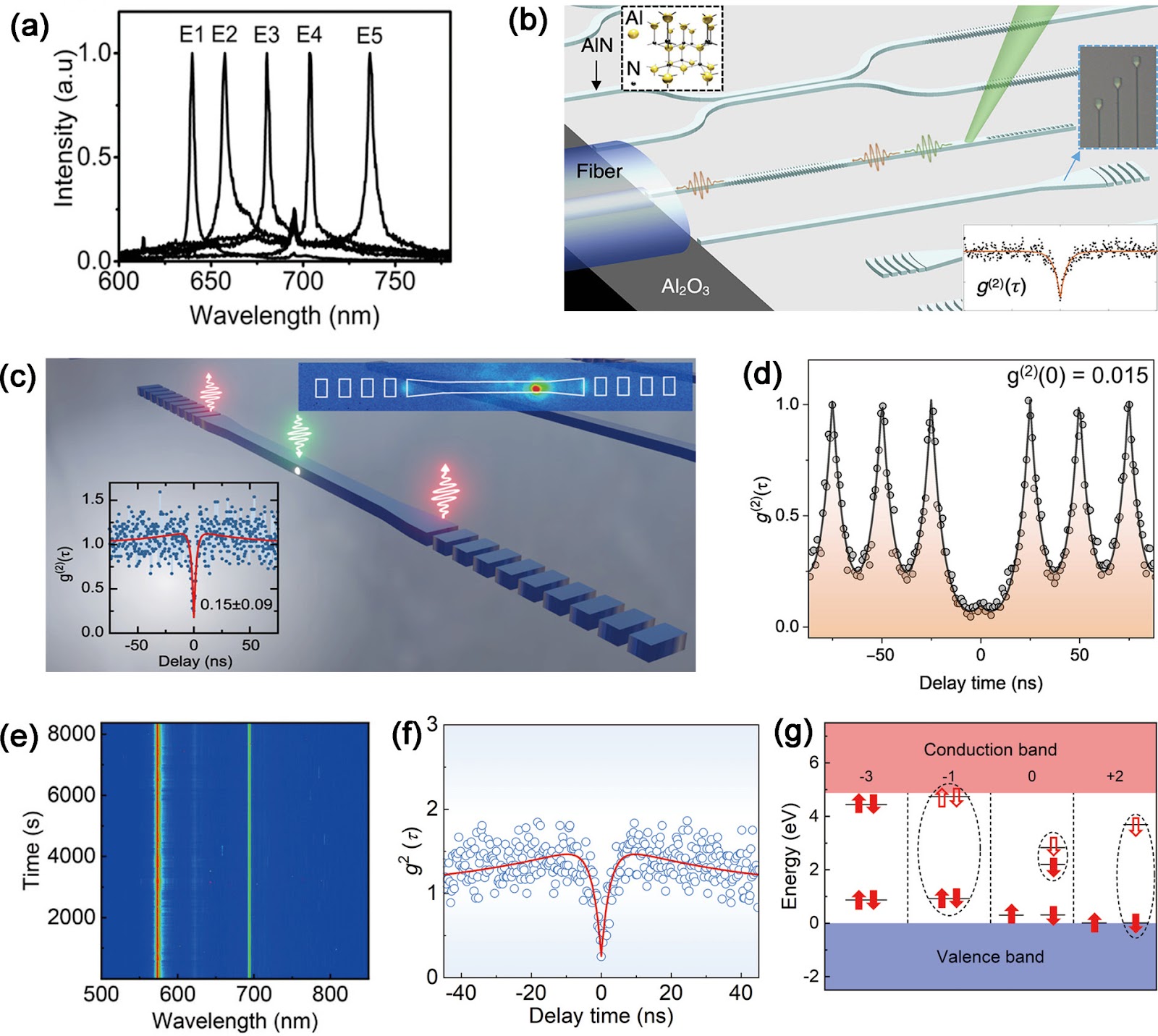
Single-photon sources are essential components for scalable quantum information technologies, with applications spanning quantum communication, quantum key distribution, quantum computing, and quantum sensing. Color centers in the solid state, such as optically active point defects, are promising candidates for the next-generation single-photon sources. Their atom-like properties enable the emission of single photons with high efficiency, purity, and indistinguishability, while their solid-state nature allows for integration into scalable quantum photonic devices. Among these, color centers in wide-bandgap semiconductors stand out as exceptionally promising single-photon emitters (SPEs), owing to their stable room-temperature (or higher) operation and wide spectral tunability. Furthermore, their compatibility with mature semiconductor technology facilitates direct integration into practical optoelectronic systems. In recent years, such defect-based SPEs have been realized in a variety of wide-bandgap semiconductors, including diamond, silicon carbide (SiC), silicon nitride (Si3N4), gallium nitride (GaN), aluminum nitride (AlN), hexagonal boron nitride (h-BN), zinc oxide (ZnO), and beta-phase gallium oxide (β-Ga2O3). This mini-review summarizes recent progress in SPEs based on wide-bandgap semiconductors and discusses their potential for integrated quantum photonic circuits.

Material Platforms for Solid-State Single-Photon Sources: Wide Bandgap Semiconductors
Graphical Abstract