SinoTechIntel Academic Portal
🏛️ Indexed Academic JournalImpact Factor: 3.8

Journal of Semiconductors (半导体学报 - 中国科学院半导体研究所)

Authoritative peer-reviewed journal in materials science, metallurgy, chemistry and engineering technologies: Journal of Semiconductors (半导体学报 - Viện Bán dẫn CAS)

Total Research Papers: 115
Access: 100% Free Open Access
Browse by Publication Year & VolumeReset All Filters ✕

Published Research PapersFiltered: Year 2025 • Vol. 32 • 8

Showing 7 of 115 peer-reviewed papers with full Graphical Abstracts.

Original ResearchVol. 32, Issue 8 • pp. 100-112DOI: 10.1088/1674-4926/25080014Jan 15, 2025

Bio-inspired spectral adaptive visual devices: A new paradigm for structure-defined functionality

Authors: BAO Youyou, ZHAO Yuhan, WU Daixuan, TIAN He

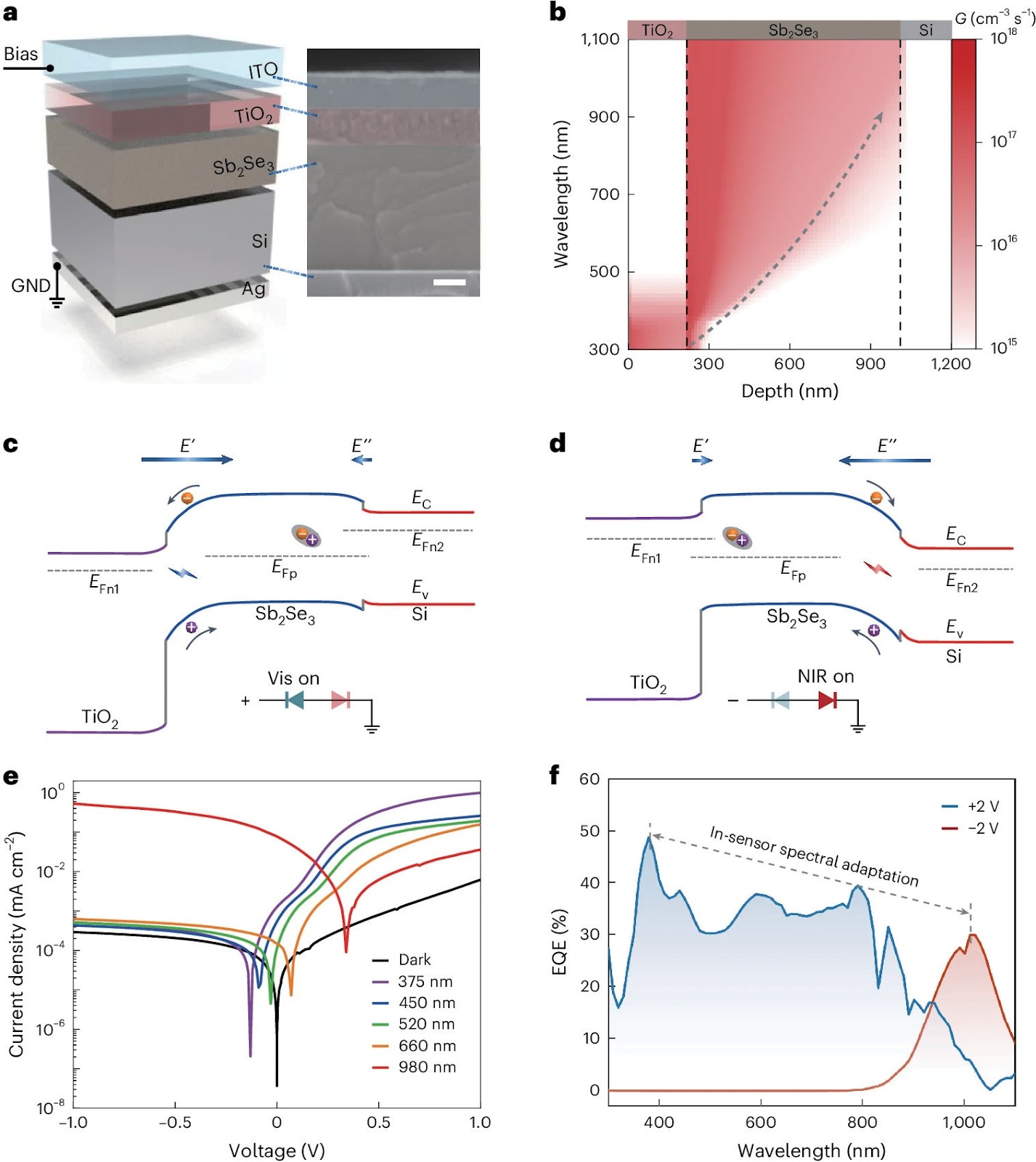
In recent years, the rapid development of artificial intelligence has driven the widespread deployment of visual systems in complex environments such as autonomous driving, security surveillance, and medical diagnosis. However, existing image sensors—such as CMOS and CCD devices—intrinsically suffer from the limitation of fixed spectral response. Especially in environments with strong glare, haze, or dust, external spectral conditions often severely mismatch the device's design range, leading to significant degradation in image quality and a sharp drop in target recognition accuracy. While algorithmic post-processing (such as color bias correction or background suppression) can mitigate these issues, algorithm approaches typically introduce computational latency and increased energy consumption, making them unsuitable for edge computing or high-speed scenarios. Achieving real-time adaptation to environmental spectral changes at the hardware level remains a major bottleneck in the intelligentization of visual systems. Zhao et al.[1] noted in their review that biomimetic sensing technologies are gradually breaking through the limitations of traditional sensors in complex environments, particularly in underwater visual systems, where structure-inspired approaches are increasingly important in defining device functionality. In 2024, Ouyang et al.[2] published a study in Nature Electronics proposing a biomimetic spectral adaptive visual device inspired by the spectral regulation mechanism of Pacific salmon. This design innovatively adopts a filterless, single-structure stacking approach, enabling the switching of the primary response spectral band within the device by adjusting the bias voltage, thereby defining spectral sensing functionality at the structural layer. The filterless stacking approach achieves 'depth-tunable' response through material heterostructures, not only avoids the volume and complexity issues of traditional multi-channel schemes but also constructs 'hardware-adaptive' sensing capabilities at the device level, opening up new avenues for the development of next-generation visual systems. The design of this spectra-adapted vision sensor draws inspiration from the efficient spectral adaptation strategies found in the biological world. Migratory salmon must transition from turbid inland freshwater to clear marine environments during their lifecycle, where the spectral compositions of visible and infrared light bands differ significantly as shown in Fig. 1(a). Salmon adjust the ratio of photoreceptor proteins with vitamin A1 and A2 structures to flexibly switch sensitivity between short-wavelength and long-wavelength light. The spectral sensitivity switching process is catalyzed by specific enzymes (such as Cyp27c1) without altering retinal structure, representing a typical 'intrinsic invariance with functional tunability'.

Bio-inspired spectral adaptive visual devices: A new paradigm for structure-defined functionality
Graphical Abstract
Original ResearchVol. 32, Issue 8 • pp. 100-112DOI: 10.1088/1674-4926/25080028Jan 15, 2025

Contact planarization and passivation lift tungsten diselenide PMOS performance

Authors: Haoyu Peng, Ping-Heng Tan, Jiangbin Wu

Two-dimensional (2D) transition metal dichalcogenides (TMDs) have superior electrical and optical properties that challenge the limits of traditional bulk semiconductors. Tungsten diselenide (WSe2) is a promising p-type channel material for advanced CMOS logic technology, but its performance has been limited by high contact resistance, poor interface quality, and unstable device behavior. This NEWS AND VIEWS article highlights two groundbreaking studies presented at the 2025 VLSI Symposium that demonstrate record performance in WSe2 p-channel transistors through innovative engineering, including surface conditioning, contact engineering, gate oxide scaling, and passivation. The studies achieve significant improvements in monolayer and multilayer WSe2 transistors, addressing key challenges and paving the way for scalable p-type transistors.

Contact planarization and passivation lift tungsten diselenide PMOS performance
Graphical Abstract
Original ResearchVol. 32, Issue 8 • pp. 100-112DOI: 10.1088/1674-4926/25080033Jan 15, 2025

A novel split gate and contact-field-plate LDMOS with enhanced BV−Ron,sp trade-off and improved FOM

Authors: Yiting Ye, Xiaoyun Huang, Yixian Song, Kai Xu

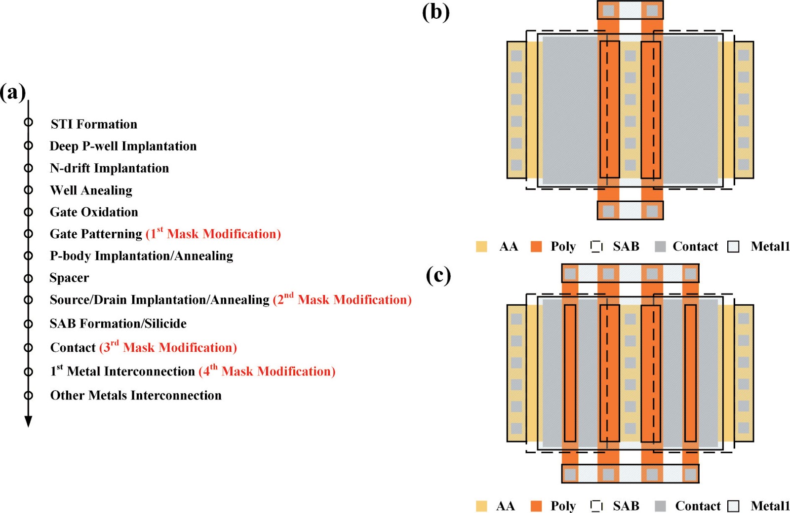
To improve the breakdown voltage (BV)−specific on-resistance (Ron,sp) trade-off and enhance manufacturability, this article proposes a novel lateral diffused metal−oxide−semiconductor (LDMOS) structure that features a split gate and split contact field plate (CFP). This novel structure requires no additional bias voltages, masks, or process steps, making it fully compatible with the bipolar-CMOS-DMOS (BCD) process flow. The physical mechanisms are elucidated through technology computer-aided design (TCAD) simulations. In the on-state, the positively biased split gate forms an accumulation layer at the drift region surface, thereby reducing Ron,sp. In the off-state, both the split gate and split CFP introduce additional electric-field peaks that smooth the lateral electric field, thus preserving a high BV. Compared with the conventional CFP-LDMOS, the proposed CFP-LDMOS achieves an 8.52% reduction in Ron,sp without compromising BV, leading to an 8.07% improvement in the figure of merit (FOM). Notably, the proposed structure can be extended to LDMOS devices across different voltage levels within BCD platforms, demonstrating its broad applicability.

A novel split gate and contact-field-plate LDMOS with enhanced BV−Ron,sp trade-off and improved FOM
Graphical Abstract
Original ResearchVol. 32, Issue 8 • pp. 100-112DOI: 10.1088/1674-4926/25080021Jan 15, 2025

Fluorine-free polymers set a new benchmark for ferroelectrics

Authors: Wentao Yao, Mingli Liang, Sasa Wang, Qiang Zhao

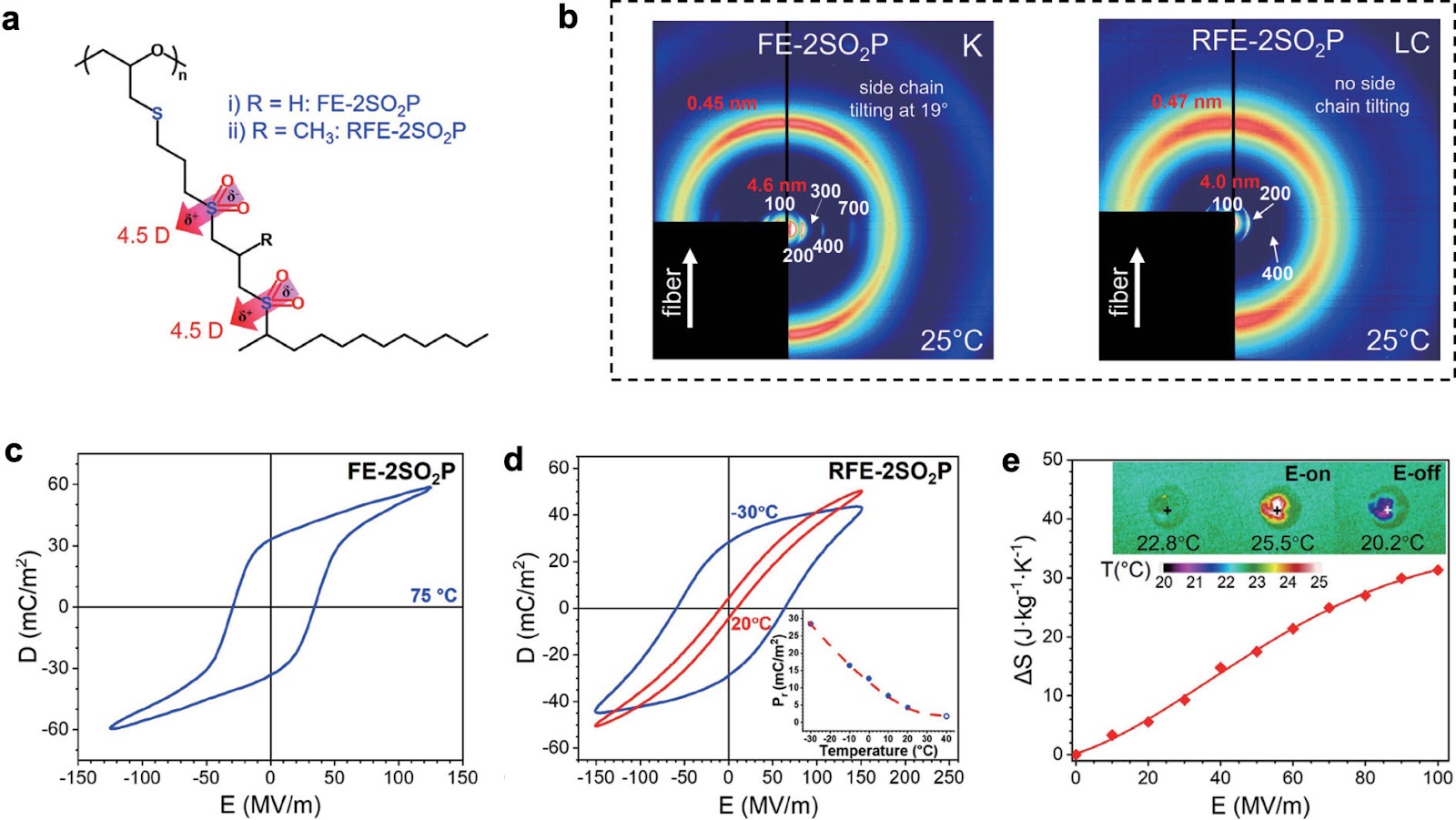
Ferroelectrics (FEs) have shown great potential in sensors, actuators, and electrocaloric cooling due to their direct cross-couplings between electric polarization and mechanical, thermal, and dielectric properties. Compared with oxide FEs, polymer FEs possess good flexibility and shape adaptability, making them promising candidates for flexible electronics and biocompatible devices. Despite decades of research, the number of FE polymers remains limited, with poly(vinylidene fluoride) (PVDF) being the most prominent due to its well-defined Curie transition and large spontaneous polarization. However, chemically modifying the semicrystalline structures of FE fluoropolymers is not only complex and costly, but also raises environmental and health concerns, as these materials are considered as "forever chemicals" due to their persistence. In pursuing fluorine-free FE polymers, the use of strong dipolar molecules to induce FE ordering is regarded as a promising strategy. This approach, initially proposed by Bohr a century ago and later validated in FE nematic and smectic A liquid crystals, relies on the alignment of rod-shaped molecules with large dipole moments (μ, μ = qd, where q is the partial charge and d is the molecular length). However, the long rod length in this system results in significant losses and heat generation during FE switching. Therefore, enhancing the partial charge (q) of compact dipolar molecules while maintaining high dipole moment density and tunable FE properties remains an ongoing challenge. Now, writing in Science, Zhu et al. tackled these problems through a unique design strategy that accommodates small, strongly dipolar disulfonyl fluorine-free polymers, –SO2CH2CHRCH2SO2– (R = –H or –CH3), which endows a high dipole moment (9 D) comparable to that of the long rod-like molecules (~10 D). The most striking feature of these polymers used in their case is that by manipulating the R group from R = –H to R = –CH3, the normal ferroelectricity (FE-2SO2P) can be simply tailored to relaxor ferroelectricity (RFE-2SO2P). Both experiments and simulations confirm that this ferroelectric order arises from the strong dipole–dipole interactions between adjacent disulfonyl groups. Remarkably, RFE-2SO2P displays exceptional electroactuation and electrocaloric performance, with an excellent electroactuation strain (–4%) and a significant electrocaloric effect (ΔS of 14.8 J·kg–1·K–1) under low electric fields, matching state-of-the-art PVDF-based tetrapolymers, highlighting its potential for advanced thermal management applications.

Fluorine-free polymers set a new benchmark for ferroelectrics
Graphical Abstract
Original ResearchVol. 32, Issue 8 • pp. 100-112DOI: 10.1088/1674-4926/25080016Jan 15, 2025

Realizing high-performance, enhanced write endurance of low-RA STT-MRAM through MgO tunnel barrier engineering

Authors: Kunkun Li, Xiaolei Yang, Junlu Gong, Shikun He

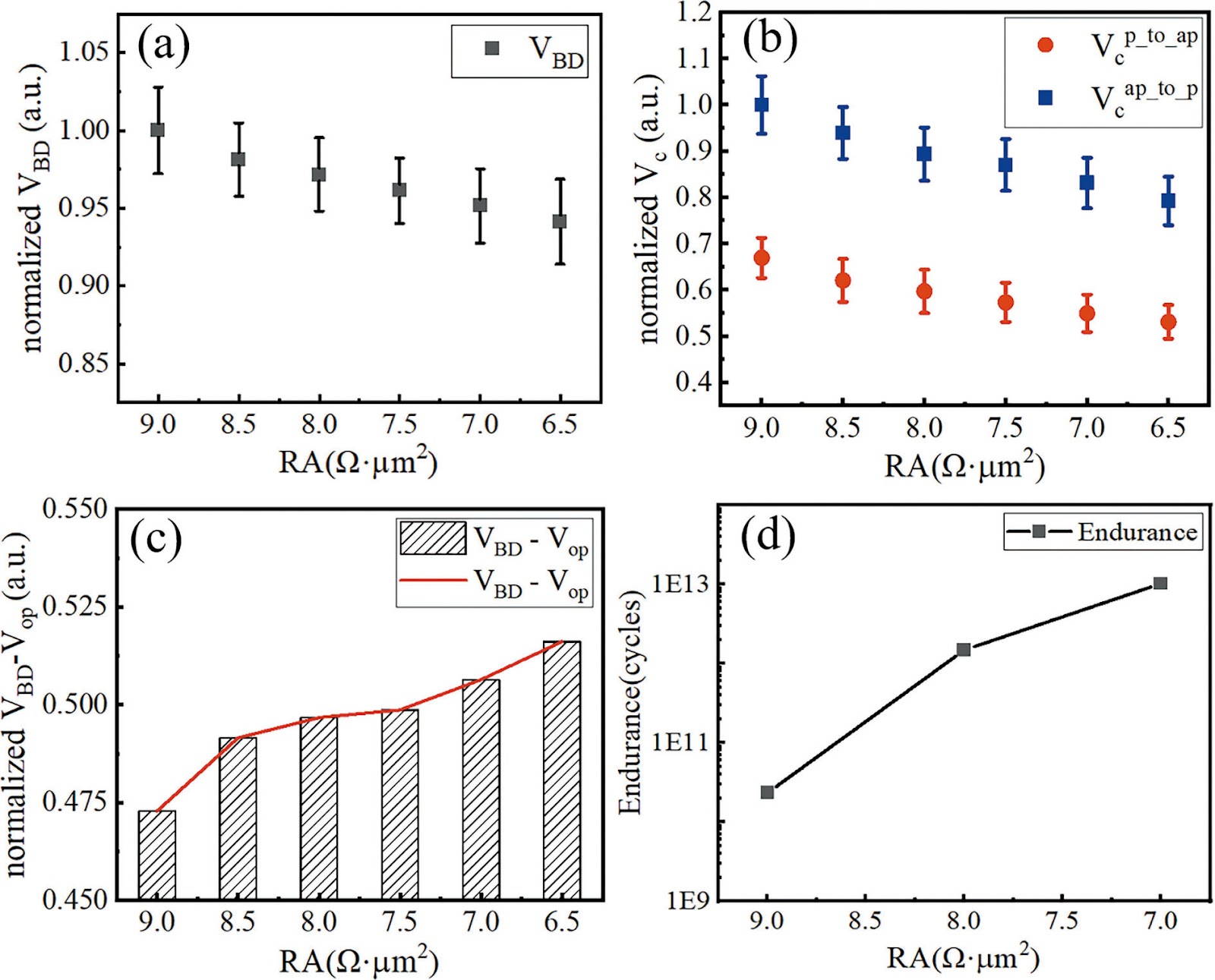
Spin-transfer-torque magnetic random-access memory (STT-MRAM), based on magnetic tunnel junctions (MTJs), is attracting significant attention for applications demanding high reliability and speed. To ensure high TMR which is essential for achieving sufficient sense margin, MTJs typically incorporate relatively thick tunnel barriers, resulting in high operating voltages. As the CMOS technology nodes advance and operating voltages decrease, reducing the MTJ switching voltage becomes imperative. However, MTJs with thinner tunnel barriers generally exhibit significantly degraded read margins and bit error rate, presenting a major challenge for achieving high-density, low-power MRAM. Here, we address this challenge through MgO tunnel barrier engineering and process optimization, successfully reducing the required MOS driving voltage while simultaneously expanding the write margin. Meanwhile, 85% array yield with sub-parts-per-million bit error rates at RA = 7 Ω·μm2 is achieved. These advancements are promising for developing high-density MRAM at advanced technology nodes.

Realizing high-performance, enhanced write endurance of low-RA STT-MRAM through MgO tunnel barrier engineering
Graphical Abstract
Original ResearchVol. 32, Issue 8 • pp. 100-112DOI: 10.1088/1674-4926/25080006Jan 15, 2025

Overcoming photovoltage deficit via phenylthiourea derivatives for efficient printed perovskite solar cells with enhanced stability

Authors: Jinlong Hu, Runxin Li, Qiongfeng Zhan, Jiajun Qin, Dadong Wen, Bing Yi, Huisheng Peng, and Zhihang Tang

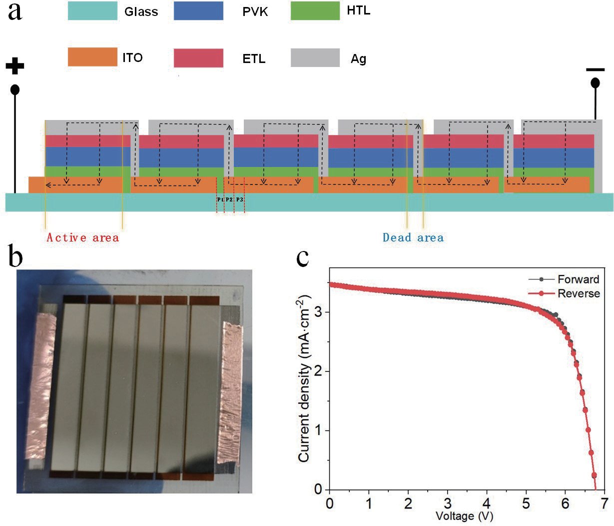
Although the certified power conversion efficiency (PCE) of single-junction perovskite solar cells (PSCs) has achieved a high level of 27%, approaching the single-crystalline silicon solar cells, the device stability remains an urgent issue to be resolved for the commercialization. Defect passivation emerged as a viable approach to enhance the operational stability of the solar devices. Herein, phenylthiourea (PhTu) derivatives are selected as effective passivation agents to enhance the optoelectronic properties of printed methylammonium lead iodide (MAPbI3) films. It is demonstrated that incorporating a small amount of 1-(4-carboxyphenyl)-2-thiourea (PhTu-COOH) significantly reduces the trap-state density and leads to longer carrier lifetime of the perovskite films. As a result, the inverted solar device made of PhTu-COOH-modified MAPbI3 perovskite film shows remarkably improved efficiency (from 17.29% to 20.22%) and obviously increased open-circuit voltage (VOC) (from 1.043 to 1.143 V), as compared with the pristine device. Moreover, the PhTu-COOH-modified PSCs exhibit enhanced operational stability due to the significantly reduced trap-state density. Finally, the optimized solar module fabricated with an active area of 11.28 cm2 delivers a high PCE of 17.07% with negligible VOC loss, demonstrating the feasibility of the blade-coating method for large-area perovskite film deposition.

Overcoming photovoltage deficit via phenylthiourea derivatives for efficient printed perovskite solar cells with enhanced stability
Graphical Abstract
Original ResearchVol. 32, Issue 8 • pp. 100-112DOI: 10.1088/1674-4926/25080038Jan 15, 2025

A low-thermal-budget MOSFET-based reservoir computing for temporal data classification

Authors: Yanqing Li, Feixiong Wang, Heyi Huang, Yadong Zhang, Xiangpeng Liang, Shuang Liu, Jianshi Tang, Huaxiang Yin

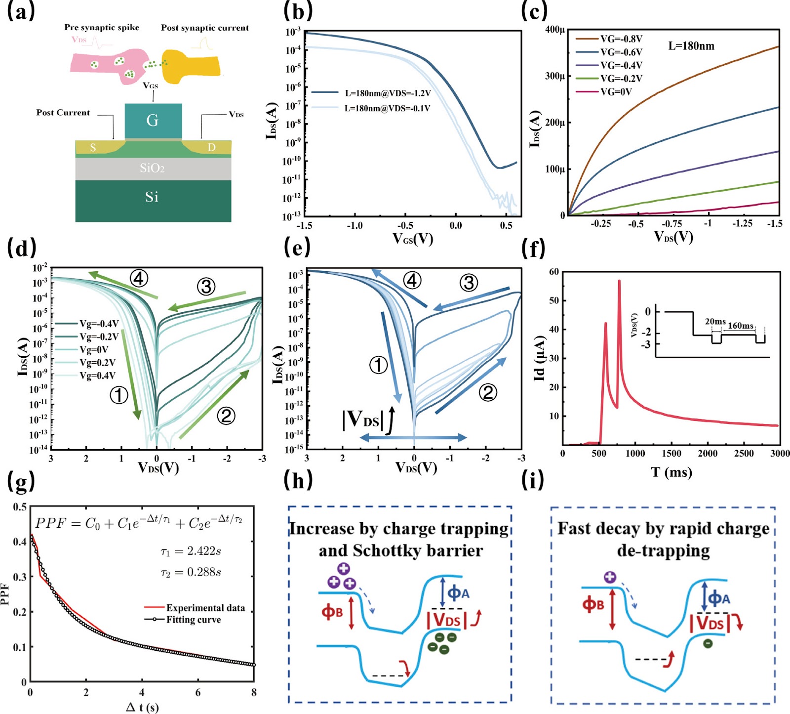
Neuromorphic devices have garnered significant attention as potential building blocks for energy-efficient hardware systems owing to their capacity to emulate the computational efficiency of the brain. In this regard, reservoir computing (RC) framework, which leverages straightforward training methods and efficient temporal signal processing, has emerged as a promising scheme. While various physical reservoir devices, including ferroelectric, optoelectronic, and memristor-based systems, have been demonstrated, many still face challenges related to compatibility with mainstream complementary metal oxide semiconductor (CMOS) integration processes. This study introduced a silicon-based schottky barrier metal−oxide−semiconductor field effect transistor (SB-MOSFET), which was fabricated under low thermal budget and compatible with back-end-of-line (BEOL). The device demonstrated short-term memory characteristics, facilitated by the modulation of schottky barriers and charge trapping. Utilizing these characteristics, a RC system for temporal data processing was constructed, and its performance was validated in a 5 × 4 digital classification task, achieving an accuracy exceeding 98% after 50 training epochs. Furthermore, the system successfully processed temporal signal in waveform classification and prediction tasks using time-division multiplexing. Overall, the SB-MOSFET's high compatibility with CMOS technology provides substantial advantages for large-scale integration, enabling the development of energy-efficient reservoir computing hardware.

A low-thermal-budget MOSFET-based reservoir computing for temporal data classification
Graphical Abstract