SinoTechIntel Academic Portal
🏛️ Indexed Academic JournalImpact Factor: 3.8

Journal of Semiconductors (半导体学报 - 中国科学院半导体研究所)

Authoritative peer-reviewed journal in materials science, metallurgy, chemistry and engineering technologies: Journal of Semiconductors (半导体学报 - Viện Bán dẫn CAS)

Total Research Papers: 115
Access: 100% Free Open Access
Browse by Publication Year & VolumeReset All Filters ✕

Published Research PapersFiltered: Year 2025 • Vol. 32 • 2

Showing 13 of 115 peer-reviewed papers with full Graphical Abstracts.

Original ResearchVol. 32, Issue 2 • pp. 100-112DOI: 10.1088/1674-4926/25020010Jan 15, 2025

A 128 × 128 monolithic spike-based hybrid-vision sensor with 0.96 Geps and 117 kfps

Authors: Huanhui Zhang, Chi Zhang, Xu Yang, Zhe Wang, Cong Shi, Runjiang Dou, Shuangming Yu, Jian Liu, Nanjian Wu, Peng Feng, Liyuan Liu

The event-based vision sensor (EVS), which can generate efficient spiking data streams by exclusively detecting motion, exemplifies neuromorphic vision methodologies. Generally, its inherent lack of texture features limits effectiveness in complex vision processing tasks, necessitating supplementary visual information. However, to date, no event-based hybrid vision solution has been developed that preserves the characteristics of complete spike data streams to support synchronous computation architectures based on spiking neural network (SNN). In this paper, we present a novel spike-based sensor with digitized pixels, which integrates the event detection structure with the pulse frequency modulation (PFM) circuit. This design enables the simultaneous output of spiking data that encodes both temporal changes and texture information. Fabricated in 180 nm process, the proposed sensor achieves a resolution of 128 × 128, a maximum event rate of 960 Meps, a grayscale frame rate of 117.1 kfps, and a measured power consumption of 60.1 mW, which is suited for high-speed, low-latency, edge SNN-based vision computing systems.

A 128 × 128 monolithic spike-based hybrid-vision sensor with 0.96 Geps and 117 kfps
Graphical Abstract
Original ResearchVol. 32, Issue 2 • pp. 100-112DOI: 10.1088/1674-4926/25020014Jan 15, 2025

GaN diodes comparative study for high energy protons detection

Authors: Matilde Siviero, Maxime Hugues, Lucas Lesourd, Eric Frayssinet, Shirley Prado de la Cruz, Sebastien Chenot, Johan-Petter Hofverberg, Marie Vidal, Jean-Yves Duboz

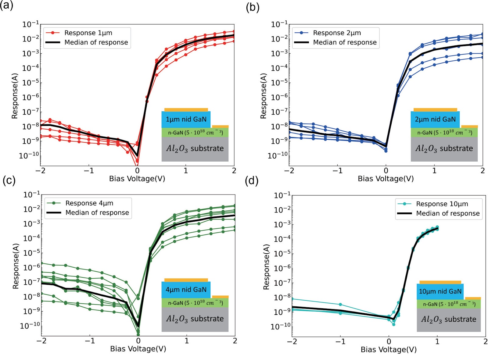
GaN diodes for high energy (64.8 MeV) proton detection were fabricated and investigated. A comparison of the performance of GaN diodes with different structures is presented, with a focus on sapphire and on GaN substrates, Schottky and pin diodes, and different active layer thicknesses. Pin diodes fabricated on a sapphire substrate are the best choice for a GaN proton detector working at 0 V bias. They are sensitive (minimum detectable proton beam <1 pA/cm2), linear as a function of proton current and fast (<1 s). High proton current sensitivity and high spatial resolution of GaN diodes can be exploited in the future for proton imaging of patients in proton therapy.

GaN diodes comparative study for high energy protons detection
Graphical Abstract
Original ResearchVol. 32, Issue 2 • pp. 100-112DOI: 10.1088/1674-4926/25020006Jan 15, 2025

Dynamic avalanche reliability enhancement of FS-IGBT under unclamped inductive switching

Authors: Jingping Zhang, Houcai Luo, Huan Wu, Bofeng Zheng, Xianping Chen

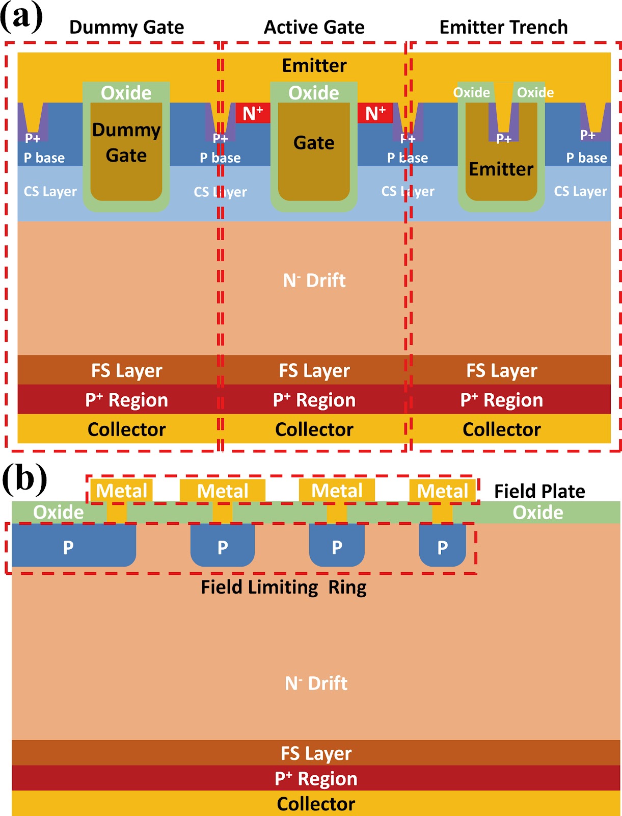
The dynamic avalanche effect is a critical factor influencing the performance and reliability of the field-stop insulated gate bipolar transistors (FS-IGBT). Unclamped inductive switching (UIS) is the primary method for testing the dynamic avalanche capability of FS-IGBTs. Numerous studies have demonstrated that factors such as device structure, avalanche-generating current filaments, and electrical parameters influence the dynamic avalanche effect of the FS-IGBT. However, few studies have focused on enhancing the avalanche reliability of the FS-IGBT by adjusting circuit parameters during operation. In this paper, the dynamic avalanche effect of the FS-IGBT under UIS conditions is comprehensively investigated through a series of comparative experiments with varying circuit parameters, including bus voltage VDC, gate voltage VG, gate resistance Rg, load inductance L, and temperature TC. Furthermore, a method to enhance the dynamic avalanche reliability of the FS-IGBT under UIS by optimizing circuit parameters is proposed. In practical applications, reducing gate voltage, increasing load inductance, and lowering temperature can effectively improve the dynamic avalanche capability of the FS-IGBT.

Dynamic avalanche reliability enhancement of FS-IGBT under unclamped inductive switching
Graphical Abstract
Original ResearchVol. 32, Issue 2 • pp. 100-112DOI: 10.1088/1674-4926/25020029Jan 15, 2025

A miniaturized wireless electrical impedance myography platform for the long-term adaptive muscle fatigue monitoring

Authors: Shanshan Yu, Yichao Gan, Feifan Song, Qiongzhang Wang, Hao Tang, Zhao Li

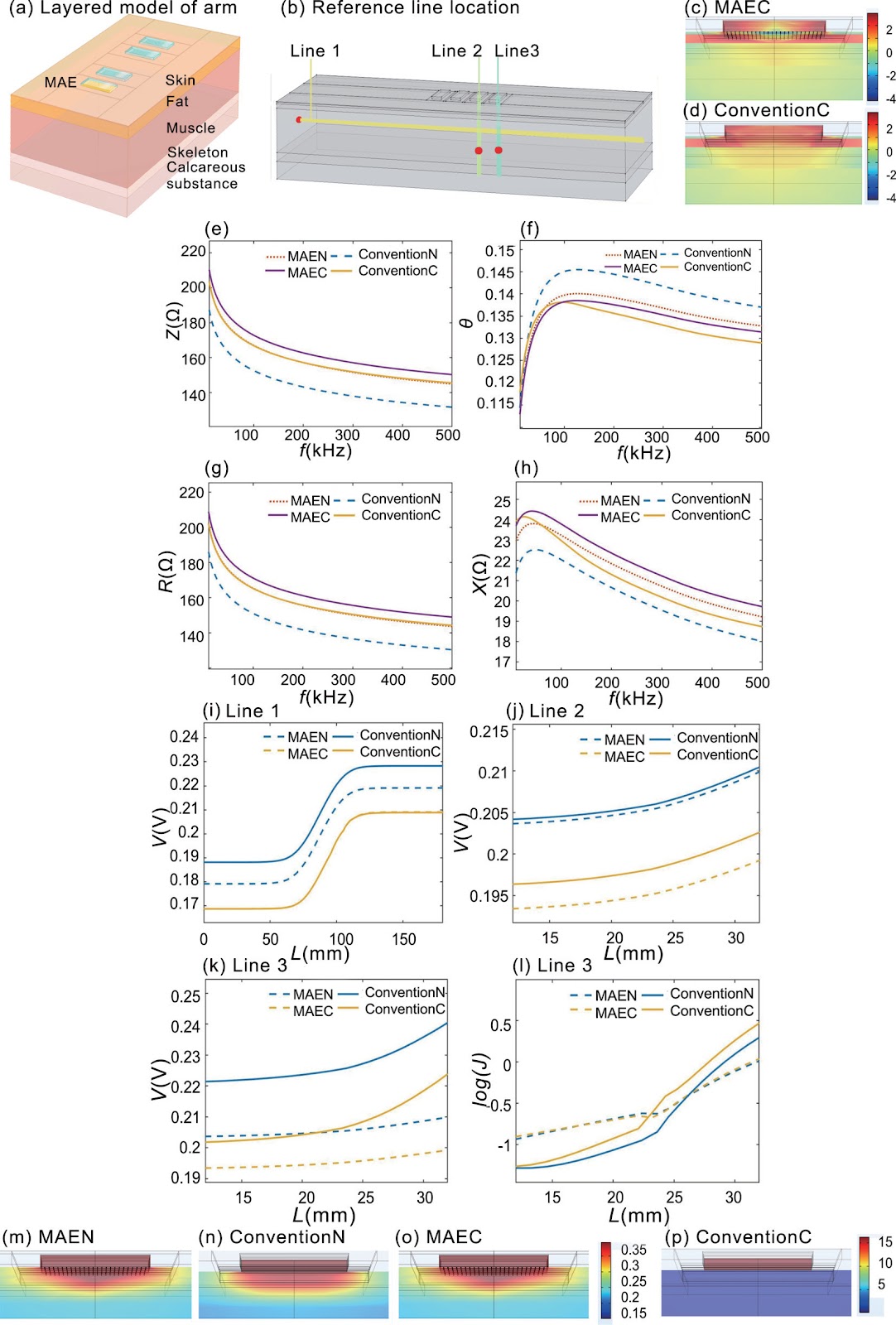
Accurate quantification of exercise interventions and changes in muscle function is essential for personalized health management. Electrical impedance myography (EIM) technology offers an innovative, noninvasive, painless, and easy-to-perform solution for muscle health monitoring. However, current EIM platforms face a number of limitations, including large device size, wired connections, and instability of the electrode-skin interface, which limit their applicability for monitoring muscle movement. In this study, a miniature wireless EIM platform with a user-friendly smartphone app is proposed and developed. The miniature, wireless, multi-frequency (20 kHz−1 MHz) EIM platform is equipped with flexible microneedle array electrodes (MAE). The advantages of MAEs over conventional electrodes were demonstrated by physical field modeling simulations and skin-electrode contact impedance comparison tests. The smartphone APP was developed to wirelessly operate the EIM platform, and to transmit and process real-time muscle impedance data. To validate its effectiveness, a seven-day adaptive fatigue training study was conducted, which demonstrated that the EIM platform was able to detect muscle adaptations and serve as a reliable indicator of fatigue. This study presents an innovative approach to applying EIM technology to muscle health monitoring and exercise testing, thereby advancing the development of personalized health management and athletic performance assessment.

A miniaturized wireless electrical impedance myography platform for the long-term adaptive muscle fatigue monitoring
Graphical Abstract
Original ResearchVol. 32, Issue 2 • pp. 100-112DOI: 10.1088/1674-4926/25020018Jan 15, 2025

Effect of grain size on the resistivity of polycrystalline 3C-SiC

Authors: Guo Li, Lei Ge, Mingsheng Xu, Jisheng Han, Xiangang Xu

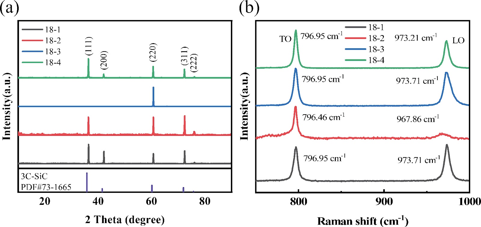
Silicon carbide offers distinct advantages in the field of power electronic devices. However, manufacturing processes remain a significant barrier to its widespread adoption. Polycrystalline SiC is less expensive and easier to produce than single crystal. But stabilizing and controlling its performance are critical challenges that must be addressed urgently. Due to its material properties and excellent performance in applications, 3C-SiC is gaining increasing attention in research. This article presents the electrical and material properties of a series of polycrystalline 3C-SiC samples and investigates their interrelationship. The samples were examined using TEM, which confirmed their polycrystalline structure. Combined with XRD and Raman spectroscopy, the grain orientations within the samples were analyzed, and the presence of stress was verified. EBSD was employed to statistically examine the grain structure and size across samples. For samples with similar doping levels, grain size is the most influential factor in determining electrical characteristics. Further EBSD measurements reveal the relationship between resistivity and grain size as log(ρ) = −1.93 + 8.67/d. These findings provide a foundation for the quantitative control and application of polycrystalline 3C-SiC. This work offers theoretical evidence for optimizing the performance tuning of 3C-SiC ceramics and enhancing their effectiveness in electronic applications.

Effect of grain size on the resistivity of polycrystalline 3C-SiC
Graphical Abstract
Original ResearchVol. 32, Issue 2 • pp. 100-112DOI: 10.1088/1674-4926/25020033Jan 15, 2025

Study of a novel SiC-based light initiated multi-gate semiconductor switch

Authors: Chongbiao Luan, Jianqiang Yuan, Hongwei Liu, Longfei Xiao, Huiru Sha, Le Xu, Yang He, Lingyun Wang, Hongtao Li, Yupeng Huang

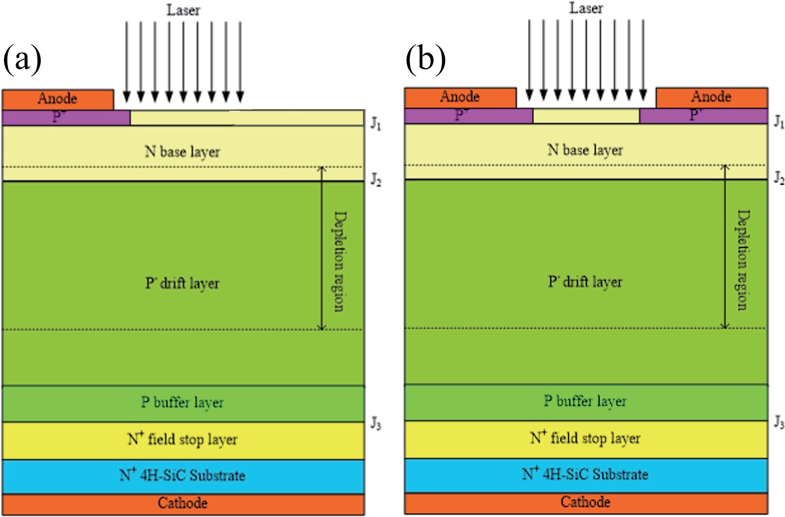
To optimize turn on velocity of the SiC LIMS, we proposed a new structure for the LIMS that incorporates an optimized n+ layer and a multi-light triggered electrode design for the anode. The chip size is 5.5 mm × 5.5 mm in dimension. The experiment results indicate that the saturation laser energy required to trigger the prepared SiC LIMS has been decreased from 1.8 mJ to 40 μJ, with the forward blocking voltage of the prepared SiC LIMSs capable of withstanding over 7000 V. The leakage current is about 0.3 μA at room temperature, and the output current density achieves 4.25 kA/cm2 (with di/dt larger than 20 kA/μs).

Study of a novel SiC-based light initiated multi-gate semiconductor switch
Graphical Abstract
Original ResearchVol. 32, Issue 2 • pp. 100-112DOI: 10.1088/1674-4926/25020031Jan 15, 2025

Breathable and skin-conformal electronic skin with dual-modality synchronous perception of pressure and temperature

Authors: Hao Zhu, Zhelin Jin, Tie Li, Guanggui Cheng, Jianning Ding

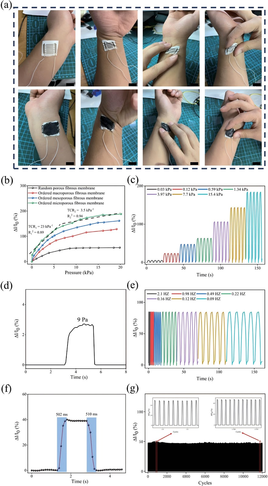
The random nanofiber distribution in traditional electrospun membranes restricts the pressure sensing sensitivity and measurement range of electronic skin. Moreover, current multimodal sensing suffers from issues like overlapping signal outputs and slow response. Herein, a novel electrospinning method is proposed to prepare double-coupled microstructured nanofibrous membranes. Through the effect of high voltage electrostatic field in the electrospinning, the positively charged nanofibers are preferentially attached to the negatively charged foam surface, forming the ordered two-dimensional honeycomb porous nanofibrous membrane with three-dimensional spinous microstructure. Compared with the conventional random porous nanofibrous membrane, the bionic two-dimensional honeycomb and three-dimensional spinous dual-coupled microstructures in the ordered porous nanofibrous membrane endows the electronic skin with significantly improved mechanical properties (maximum tensile strain increased by 77% and fatigue resistance increased by 35%), air permeability (water vapor transmission rate increased by 16%) and sensing properties (pressure sensitivity increased by 276% and detection range increased by 137%). Furthermore, the electronic skin was constructed by means of a conformal composite ionic liquid functionalized nanofibrous membrane, and the real-time and interference-free dual-signal monitoring of pressure and temperature (maximum temperature coefficient of resistance: −0.918 °C−1) was realized.

Breathable and skin-conformal electronic skin with dual-modality synchronous perception of pressure and temperature
Graphical Abstract
Original ResearchVol. 32, Issue 2 • pp. 100-112DOI: 10.1088/1674-4926/25020025Jan 15, 2025

Mesa-structured AlGaAsSb APD: dark current and noise analysis

Authors: Yuhang He, Rui Wang, Yan Liang, Yingqiang Xu, Guowei Wang, Haiqiao Ni, Shuo Wang, Zhichuan Niu, Xiaohong Yang

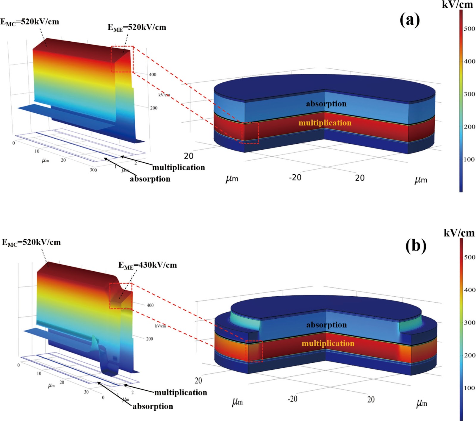
Avalanche photodiode (APD) is a kind of photodetector with important applications in optical communication, light detection and ranging (LIDAR) and other fields. APDs fabricated using the recently developed AlGaAsSb as the multiplication material exhibit excellent noise performance. In this work, we report a low-noise separate absorption, grading, charge, and multiplication (SAGCM) InGaAs/AlGaAsSb APD operating at 1550 nm. A double-mesa structure was fabricated to reduce the dark current. Numerical simulations were conducted to compare two different mesa-structured APDs. By analyzing the electric field distribution, it was found that the electric field at the edge of the multiplication region in the double-mesa APD is nearly 100 kV/cm lower than that of the single-mesa structure. Experimental results demonstrate that after device punch-through, the double-mesa APD’s dark current can be reduced by up to four times compared to the single-mesa APD. Quantitative analysis of the dark current components in the AlGaAsSb APD further confirms that the low sidewall electric field in the double-mesa structure effectively suppresses the trap-assisted tunneling. Additionally, noise measurements indicate a k-value of approximately 0.014, which is significantly lower than that of traditional multiplication materials. This work provides preliminary validation for further performance improvements in low noise and low dark current AlGaAsSb APDs.

Mesa-structured AlGaAsSb APD: dark current and noise analysis
Graphical Abstract
Original ResearchVol. 32, Issue 2 • pp. 100-112DOI: 10.1088/1674-4926/25020008Jan 15, 2025

Band alignment of SnO/β-Ga2O3 heterojunction and its electrical properties for power device application

Authors: Xia Wu, Chenyang Huang, Xiuxing Xu, Jun Wang, Xinwang Yao, Yanfang Liu, Xiujuan Wang, Chunyan Wu, Linbao Luo

In this study, we present the fabrication of vertical SnO/β-Ga2O3 heterojunction diode (HJD) via radio frequency (RF) reactive magnetron sputtering. The valence and conduction band offsets between β-Ga2O3 and SnO are determined to be 2.65 and 0.75 eV, respectively, through X-ray photoelectron spectroscopy, showing a type-Ⅱ band alignment. Compared to its Schottky barrier diode (SBD) counterpart, the HJD presents a comparable specific ON-resistances (Ron,sp) of 2.8 mΩ·cm² and lower reverse leakage current (IR), leading to an enhanced reverse blocking characteristics with breakdown voltage (BV) of 1675 V and power figure of merit (PFOM) of 1.0 GW/cm². This demonstrates the high quality of the SnO/β-Ga2O3 heterojunction interface. Silvaco TCAD simulation further reveals that electric field crowding at the edge of anode for the SBD was greatly depressed by the introduction of SnO film, revealing the potential application of SnO/β-Ga2O3 heterojunction in the future β-Ga2O3-based power devices.

Band alignment of SnO/β-Ga2O3 heterojunction and its electrical properties for power device application
Graphical Abstract
Original ResearchVol. 32, Issue 2 • pp. 100-112DOI: 10.1088/1674-4926/25020028Jan 15, 2025

A leap forward in compute-in-memory system for neural network inference

Authors: Liang Chu, Wenjun Li

Developing efficient neural network (NN) computing systems is crucial in the era of artificial intelligence (AI). Traditional von Neumann architectures have both the issues of "memory wall" and "power wall", limiting the data transfer between memory and processing units. Compute-in-memory (CIM) technologies, particularly analogue CIM with memristor crossbars, are promising because of their high energy efficiency, computational parallelism, and integration density for NN computations. In practical applications, analogue CIM excels in tasks like speech recognition and image classification, revealing its unique advantages. For instance, it efficiently processes vast amounts of audio data in speech recognition, achieving high accuracy with minimal power consumption. In image classification, the high parallelism of analogue CIM significantly speeds up feature extraction and reduces processing time. With the boosting development of AI applications, the demands for computational accuracy and task complexity are rising continually. However, analogue CIM systems are limited in handling complex regression tasks with needs of precise floating-point (FP) calculations. They are primarily suited for the classification tasks with low data precision and a limited dynamic range. A novel analogue-digital unified CIM architecture (named as AnDi) has been developed by integrating the analogue and digital computing cores, which aims to address the above challenges of analogue CIM. The key component is the dual-domain floating-point (DDFP) processor, which serves as a universal data type to represent both FP and integer (INT) numbers. This processor enables FP compatibility regardless of the native capabilities of analogue CIM or digital cores. The DDFP data structure consists of an INT tensor for the feature map and an FP scale. The DDFP processor manages data flow between the analogue and digital domains, performing quantization or dequantization operation. This effectively decouples the NN algorithm from the underlying hardware, enabling more general NN computation. The training process for the top-level algorithm can proceed without considering specific hardware architectures, as all data-scaling operations are handled at the hardware level. To maximize the potential of AnDi architecture, several strategies have been proposed. The fine-grained dual-domain mapping divides weight matrices larger than analogue CIM arrays into smaller ones. Weights are allocated to either digital or analogue cores based on their size. Low-parallel weight blocks are assigned to digital cores, thus maximizing the utilization rates of digital multiply-accumulate (MAC) cores. This approach enhances system-level energy efficiency by avoiding weight splits into additional blocks within the same layer, thereby reducing memory management overhead. The NN feature-enhancing technique addresses the noise accumulation issue in analogue CIM. Lightweight enhancing layers are integrated into the network and deployed on noise-free digital cores for inference.

A leap forward in compute-in-memory system for neural network inference
Graphical Abstract
Original ResearchVol. 32, Issue 2 • pp. 100-112DOI: 10.1088/1674-4926/25020024Jan 15, 2025

Boosting photoelectrochemical performance on α-Ga2O3 nanowire arrays by indium cation doping for self-powered ultraviolet detection

Authors: Junjun Xue, Jiyuan Huang, Kehan Li, Ping Liu, Yan Gu, Ting Zhi, Yan Dong, Jin Wang

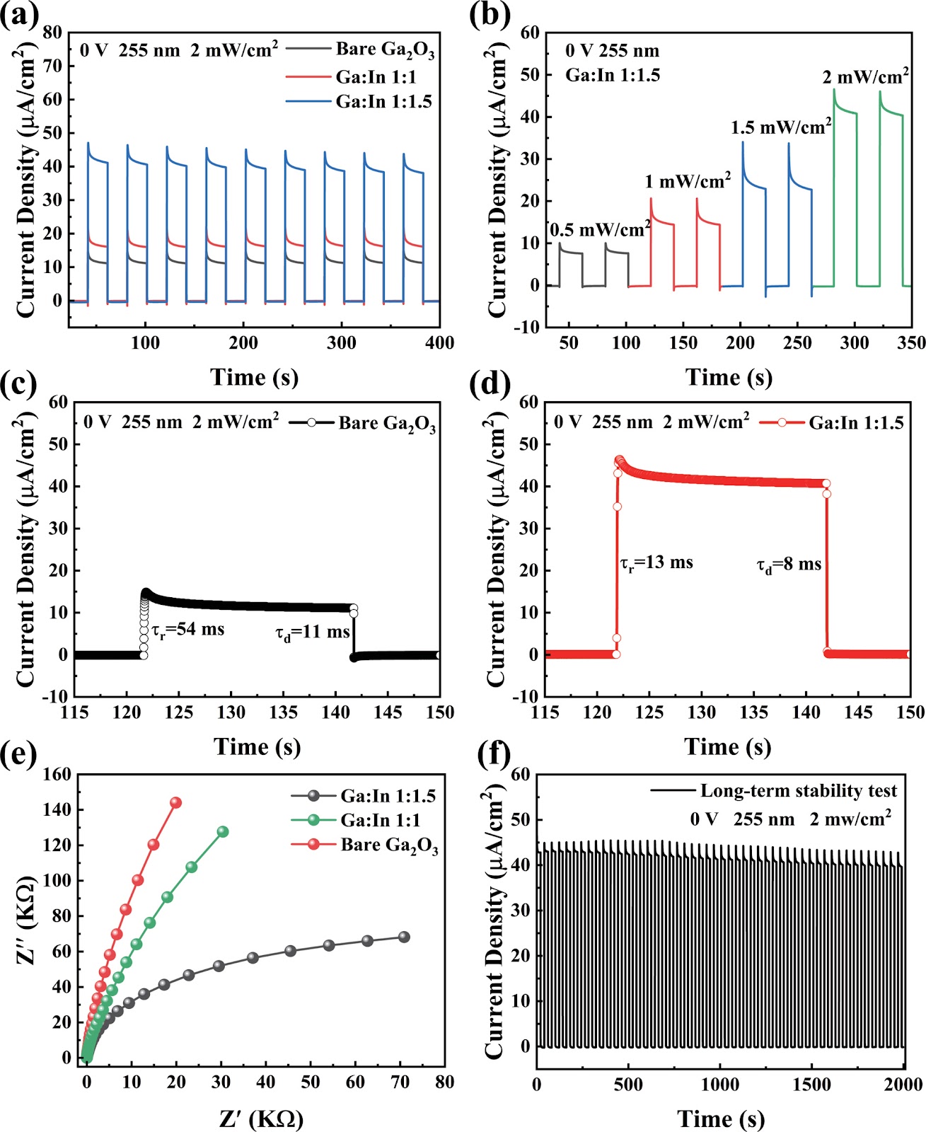
Low power consumption, high responsivity, and self-powering are key objectives for photoelectrochemical ultraviolet detectors. In this research, In-doped α-Ga2O3 nanowire arrays were fabricated on fluorine-doped tin oxide (FTO) substrates through a hydrothermal approach, with subsequent thermal annealing. These arrays were then used as photoanodes to construct a ultraviolet (UV) photodetector. In doping reduced the bandgap of α-Ga2O3, enhancing its absorption of UV light. Consequently, the In-doped α-Ga2O3 nanowire arrays exhibited excellent light detection performance. When irradiated by 255 nm deep ultraviolet light, they obtained a responsivity of 38.85 mA/W. Moreover, the detector's response and recovery times are 13 and 8 ms, respectively. The In-doped α-Ga2O3 nanowire arrays exhibit a responsivity that is about three-fold higher than the undoped one. Due to its superior responsivity, the In-doped device was used to develop a photoelectric imaging system. This study demonstrates that doping α-Ga2O3 nanowire with indium is a potent approach for optimizing their photoelectrochemical performance, which also has significant potential for optoelectronic applications.

Boosting photoelectrochemical performance on α-Ga2O3 nanowire arrays by indium cation doping for self-powered ultraviolet detection
Graphical Abstract
Original ResearchVol. 32, Issue 2 • pp. 100-112DOI: 10.1088/1674-4926/25020011Jan 15, 2025

A 32Gb/s digital-assisted PAM-4 DFB laser driver in 28-nm CMOS

Authors: Yang Min, Nan Qi, Yihan Chen, Minye Zhu, Guike Li, Yonghui Lin, Zhao Zhang, Jian Liu, Nanjian Wu, Jingbo Shi, Frank F. Shi, Liyuan Liu

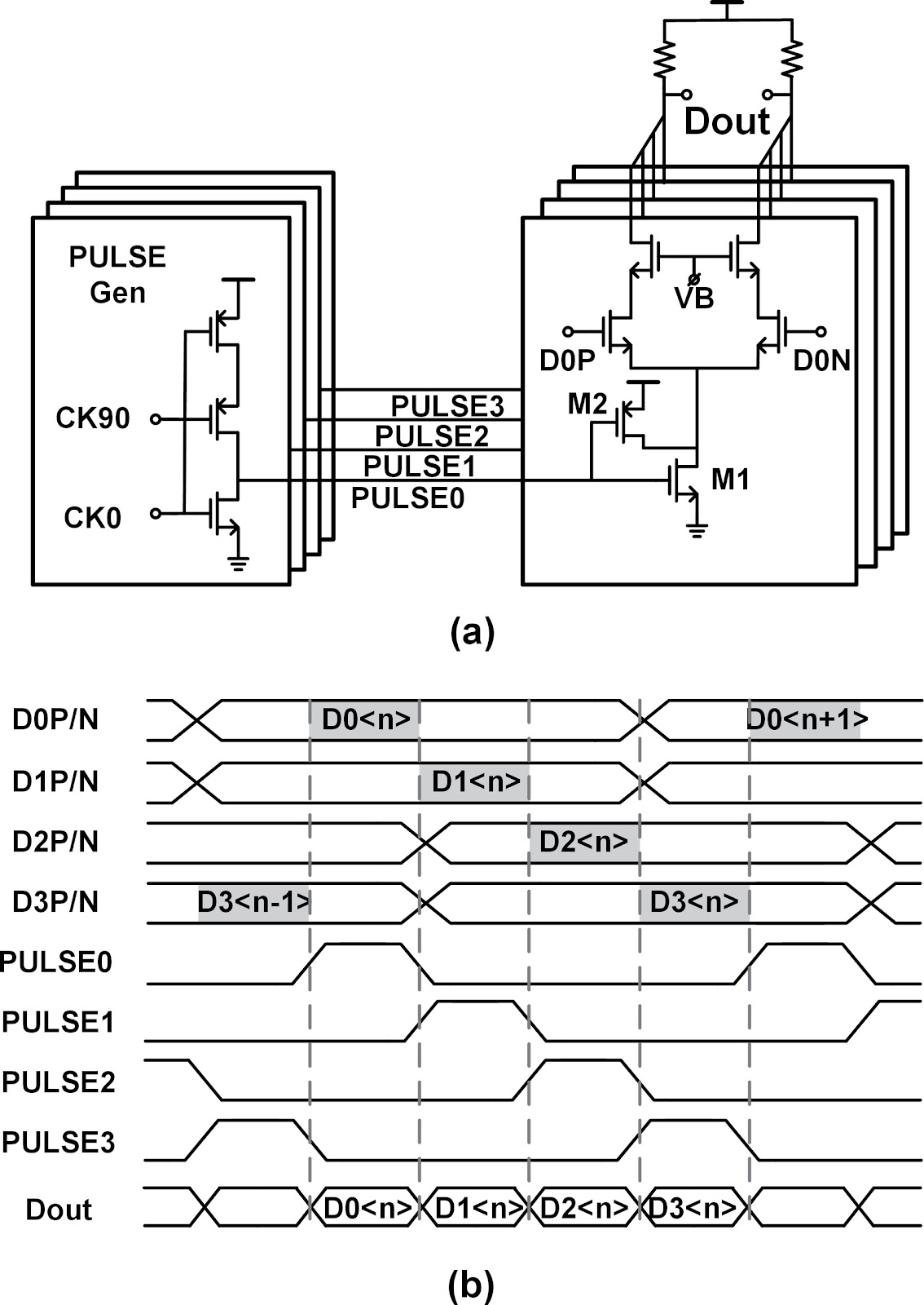
This paper presents a 4-level pulse amplitude modulation (PAM-4) distributed feedback (DFB) laser driver. The driver adopts a digital slicing architecture to achieve high linearity by adjusting the weights of three thermometer-coded main paths. An efficient-biased output stage structure is proposed to reduce power consumption while avoiding the degradation of output node bandwidth typically induced by parasitic capacitance in high-current bias path. A two-tap linear and nonlinear feed-forward equalizer (FFE) is implemented in the digital domain to extend bandwidth limitations and compensate for the dynamic nonlinearity of the DFB laser. The nonlinear FFE is realized at the cost of lower power consumption and smaller area by utilizing the simultaneity of low-speed parallel data. The chip is fabricated in 28 nm CMOS process. Measurement results indicate that, with a laser bias current of 40 mA, a modulation current of 20 mApp, and an operating rate of 32 Gb/s PAM-4, the overall power consumption of the chip is 372 mW, corresponding to an energy efficiency of 11.6 pJ/b.

A 32Gb/s digital-assisted PAM-4 DFB laser driver in 28-nm CMOS
Graphical Abstract
Original ResearchVol. 32, Issue 2 • pp. 100-112DOI: 10.1088/1674-4926/25020034Jan 15, 2025

Robotic computing system and embodied AI evolution: an algorithm-hardware co-design perspective

Authors: YAN Longke, ZHAO Xin, YANG Bohan, WU Yongkun, DAI Guangnan, LI Jiancong, TSUI Chi-Ying, CHENG Kwang-Ting, ZHANG Yihan, TU Fengbin

Robotic computing systems play an important role in enabling intelligent robotic tasks through intelligent algorithms and supporting hardware. In recent years, the evolution of robotic algorithms indicates a roadmap from traditional robotics to hierarchical and end-to-end models. This algorithmic advancement poses a critical challenge in achieving balanced system-wide performance. Therefore, algorithm-hardware co-design has emerged as the primary methodology, which analyzes algorithm behaviors on hardware to identify common computational properties. These properties can motivate algorithm optimization to reduce computational complexity and hardware innovation from architecture to circuit for high performance and high energy efficiency. We then reviewed recent works on robotic and embodied AI algorithms and computing hardware to demonstrate this algorithm-hardware co-design methodology. In the end, we discuss future research opportunities by answering two questions: (1) how to adapt the computing platforms to the rapid evolution of embodied AI algorithms, and (2) how to transform the potential of emerging hardware innovations into end-to-end inference improvements.

Robotic computing system and embodied AI evolution: an algorithm-hardware co-design perspective
Graphical Abstract