SinoTechIntel Academic Portal
🏛️ Indexed Academic JournalImpact Factor: 3.8

Journal of Semiconductors (半导体学报 - 中国科学院半导体研究所)

Authoritative peer-reviewed journal in materials science, metallurgy, chemistry and engineering technologies: Journal of Semiconductors (半导体学报 - Viện Bán dẫn CAS)

Total Research Papers: 115
Access: 100% Free Open Access
Browse by Publication Year & VolumeReset All Filters ✕

Published Research PapersFiltered: Year 2025 • Vol. 32 • 5

Showing 6 of 115 peer-reviewed papers with full Graphical Abstracts.

Original ResearchVol. 32, Issue 5 • pp. 100-112DOI: 10.1088/1674-4926/25050007Jan 15, 2025

Innovative applications of fullerenes in perovskite solar cells

Authors: Tianhua Liu, Xiangyue Meng, Chunru Wang

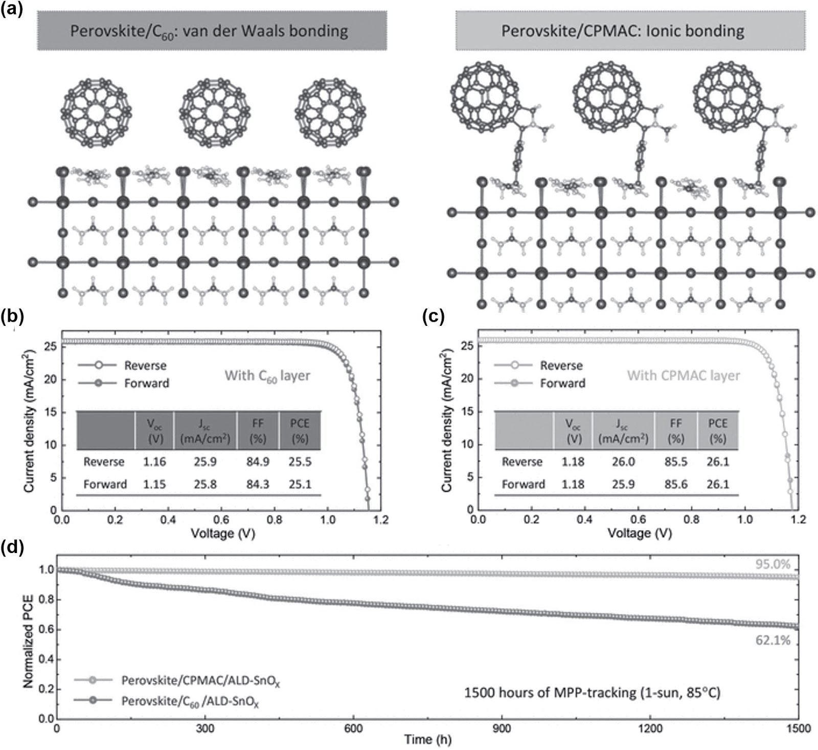
Perovskite solar cells (PSCs) have emerged as a highly promising photovoltaic technology, achieving power conversion efficiencies exceeding 25%. However, stability remains a critical challenge due to degradation under heat, moisture, and operational stress. Fullerenes, such as C60 and PCBM, have been widely used as electron-transport materials in PSCs, but they offer limited interfacial stabilization. Recent research focuses on innovative fullerene-based materials that enhance electron conduction and protect the perovskite interface. A cutting-edge approach involves magnetic endohedral metallofullerenes, such as Nd@C82, integrated into a polymer matrix to form a robust interface layer. This composite interlayer facilitates ultrafast electron transport, provides in-situ encapsulation, and induces interface polarization for efficient charge separation, thereby improving both efficiency and stability.

Innovative applications of fullerenes in perovskite solar cells
Graphical Abstract
Original ResearchVol. 32, Issue 5 • pp. 100-112DOI: 10.1088/1674-4926/25050012Jan 15, 2025

High-precision ADC design techniques in ISSCC 2025

Authors: Bingrui Li, Zongnan Wang, Xiyuan Tang

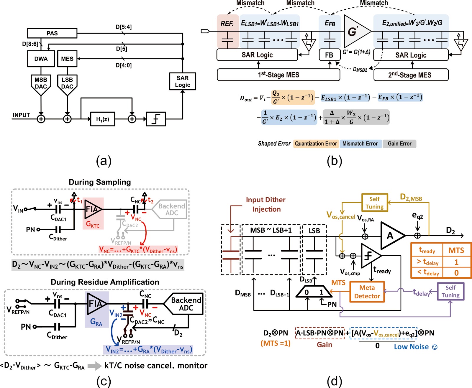
High-precision analog-to-digital converters (ADCs) serve as fundamental components in modern electronic systems, bridging the physical analog world and digital intelligence. They find ubiquitous applications across diverse domains, ranging from the Internet of Things (IoT) to embodied artificial intelligence systems. Achieving high precision necessitates various circuit techniques including high-performance amplifiers and advanced calibration schemes. Furthermore, the evolution of ADC architectures has gradually elevated the significance of peripheral circuitry co-design in optimizing system-level performance metrics. In ISSCC 2025, several techniques are proposed to address these challenges. Amplifiers are typically the main bottleneck in the performance and efficiency of high-precision ADCs. The open-loop charge-transfer amplifier is a promising candidate for its good efficiency. However, conventional ones suffer from poor power supply rejection ratio (PSRR) and common-mode rejection, leading to signal-to-noise ratio (SNR) and robustness challenges. To overcome these problems, Huang et al. proposed a floating charge transfer topology, where the transistors are powered by a floating capacitor. As input and output currents of the capacitor are forced to be equal, supply noise will be forced to circulate within the amplifier. The post-layout simulation shows that the gain variation is limited to ±2.7% over process-voltage-temperature (PVT) variations without any trimming. Fabrication-induced variations, such as inter-stage gain errors and capacitor mismatches, can degrade ADC performance. Researches presented several improvements in dynamic element matching (DEM) and calibration techniques this year to address these challenges. Zhao et al. implemented a 120 dB signal-to-noise-and-distortion ratio (SNDR) 189 dB Schreier figure-of-merit (FoMs) noise-shaping (NS) successive approximation register (SAR) ADC with hybrid mismatch shaping and system-level chopping. The 8b capacitor digital-to-analog converter (CDAC) is segmented into 3 most significant bits (MSBs) with 8 equal capacitors and 5 binary-weighted least significant bits (LSBs). Data weighted averaging (DWA) and mismatch error shaping (MES) are applied to the MSBs and LSBs respectively, increasing the quantizer resolution effectively. System-level chopping is adopted to eliminate the offset, 1/f noise, and the VCM induced CDAC nonlinearity simultaneously. In Ref. [4], Gao et al. extended the MES to multi-stage applications and presented a 93.3 dB-SNDR 180.4 dB-FoMs calibration-free NS pipelined-SAR ADC with cross-stage gain-mismatch-error-shaping technique. An extra capacitor CFB is added in the 1st-stage CDAC to serve as the mismatch reference of the 2nd-stage CDAC and residue amplifier. By involving CFB in the MES procedure of the 1st stage, both the capacitor mismatch of two stages and the gain error can be shaped and eliminated. This work further solved the MES saturation problem by pre-comparison during sampling. Sampling noise is a critical problem for discrete-time (DT) ADCs. Wang et al. propose...

High-precision ADC design techniques in ISSCC 2025
Graphical Abstract
Original ResearchVol. 32, Issue 5 • pp. 100-112DOI: 10.1088/1674-4926/25050016Jan 15, 2025

A RISC-V 32-bit microprocessor on two-dimensional semiconductor platform

Authors: Di Zhang, Yang Li

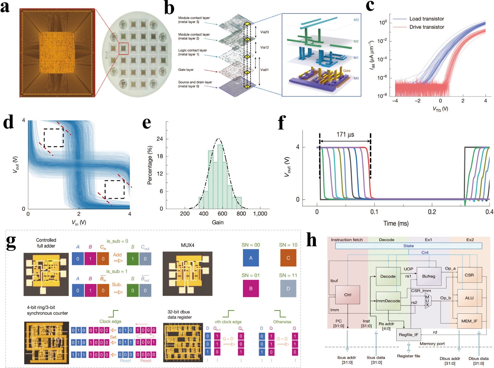
With the rapid development of information technology, the demand for high-performance and low-power microprocessors continues to grow. Traditional silicon-based semiconductor technologies have encountered numerous bottlenecks in performance enhancement, such as drain-induced barrier lowering, reduced mobility caused by interface scattering, and limited current on/off ratios. These limitations have spurred researchers to seek out new materials. Two-dimensional (2D) semiconductors have emerged as a promising solution due to their atomic thickness, excellent electrical properties, and mechanical flexibility. Despite significant progress in the wafer-scale growth and device fabrication of 2D materials, integrating them into large-scale functional circuits remains a challenge. Recently, Zhou and colleagues achieved a significant breakthrough in this area by successfully developing the RV32-WUJI, a RISC-V 32-bit microprocessor based on 5900 molybdenum disulfide (MoS₂) transistors, demonstrating the great potential of 2D semiconductors in complex circuits. This microprocessor achieved a manufacturing yield of 99.77% and a low power consumption of 0.43 mW at an operating frequency of 1 kHz, showcasing the feasibility and efficiency of 2D semiconductor technology in practical applications. In the manufacturing process, the researchers use a 4-inch MoS₂ wafer to successfully fabricate the RV32-WUJI microprocessor. The microprocessor employs a top-gate field-effect transistor (FET) structure that is compatible with mainstream silicon CMOS technology. The manufacturing process includes front-end-of-line (FEOL) and back-end-of-line (BEOL) processes. By employing a systematic co-optimization strategy and machine learning to analyze the impact of each process step on device performance, the researchers achieve a high yield (99.92% for transistors) and low power consumption (0.43 milliwatts at 1 kHz) in the wafer-scale 2D integrated circuit manufacturing. Fig. 1(a) presents the optical microscopic images of the entire wafer and a single RV32-WUJI chip, highlighting the complexity and scale of the manufacturing. Fig. 1(b) clearly illustrates the four-layer structure of the microprocessor, including the source and drain layer (M0), gate layer, logic connection layer (M1), and module connection layers (M2 and M3), clarifying the functions and interconnections of each layer. This four-layer structure is crucial for achieving the high integration density and functionality required for complex microprocessors. The use of a top-gate structure allows for better control over the electrical properties of the MoS2 transistors, which is essential for high-performance digital circuits. Additionally, the researchers optimize the process flow to ensure compatibility with existing CMOS technologies, making the integration of 2D materials more feasible.

A RISC-V 32-bit microprocessor on two-dimensional semiconductor platform
Graphical Abstract
Original ResearchVol. 32, Issue 5 • pp. 100-112DOI: 10.1088/1674-4926/25050802Jan 15, 2025

Preface to Special Topic on Integrated Circuits, Technologies and Applications 2024

Authors: Zheng Wang, Yan Lu

This Special Topic of the Journal of Semiconductors (JOS) features expanded versions of key articles presented at the 2024 IEEE International Conference on Integrated Circuits Technologies and Applications (ICTA), held in Hangzhou, Zhejiang, China, from October 25 to 27, 2024. Among the 115 papers presented, four high-quality articles were selected covering RF IC, Analog IC, and Wireline IC. The RF IC papers include a battery-free wireless temperature sensing chip for food production environment monitoring and a two-way series Doherty power amplifier with distributed impedance inverting network for millimeter-wave applications. The Analog IC paper presents a high-precision bandgap reference with ultra-low temperature coefficient and line sensitivity for battery management systems. The Wireline IC paper (not detailed in the excerpt) completes the selection. These articles represent state-of-the-art advancements in integrated circuit design and technology.

Preface to Special Topic on Integrated Circuits, Technologies and Applications 2024
Graphical Abstract
Original ResearchVol. 32, Issue 5 • pp. 100-112DOI: 10.1088/1674-4926/25050801Jan 15, 2025

Preface to the Special Issue on Updated Progresses in Perovskite Solar Cells

Authors: Jingbi You

Metal halide perovskites, as a novel class of semiconductor optoelectronic materials, combine the excellent optoelectronic properties of inorganic semiconductors with the advantages of low-cost, printable fabrication typical of organic semiconductors, making them a cutting-edge research focus in the field of semiconductor optoelectronic devices. In recent years, significant progress has been made in perovskite solar cell research: the efficiency of single-junction cells has reached 27%, module efficiency at the square-meter scale has exceeded 18%, laboratory-tested stability has achieved 10,000 h, extrapolated stability has reached several tens of thousands of hours, and GW-scale production lines have been preliminarily established. Perovskite-based tandem cells are flourishing, with perovskite/crystalline silicon tandem efficiency approaching 35%. Wafer-sized perovskite/silicon tandems have already surpassed the efficiency of single-junction silicon cells, while important advancements have also been made in perovskite/perovskite, perovskite/organic, and perovskite/copper indium gallium selenide (CIGS) tandem cells. From these progresses, we fully believe perovskite solar cells is very promising photovoltaic technology. In this special topic, we organized a Special Issue to summarize updated progresses in perovskite solar cells, and we are grateful to invite 12 researchers who are working in perovskite solar cells to summarize recent important progresses, contribute their research results or highlight recent outstanding work in perovskite solar cells. Specifically, we have 4 reviews, including the flexible perovskite solar cells and its potential application in aerospace, integrated perovskite-organic solar cells, NiOx for perovskite solar cells, and high performance perovskite material FAPbI3, in addition, 5 research papers covering perovskite/perovskite tandem solar cells, lead free perovskite solar cells, passivation and additive for enhancing device performance. We also invited two highlights, one is perovskite/silicon tandem, which is one of the most important topic now in photovoltaic technology, not only the researchers in university or institute working in this topic, a lot of leading silicon companies are immerging into this hot area; the other one is the homogenizing of perovskite, which should be the next critical strategy for further improving the efficiency and also the stability of perovskite solar cells. Last but not at least, a comment paper is about Interface energetics in organic and perovskite semiconductor solar cells. We sincerely hope that the readers working in this hot area could benefit a lot from the published papers in this Special Issue.
Preface to the Special Issue on Updated Progresses in Perovskite Solar Cells
Graphical Abstract
Original ResearchVol. 32, Issue 5 • pp. 100-112DOI: 10.1088/1674-4926/25050011Jan 15, 2025

Machine learning facilitates the development of interconnecting layers for perovskite/silicon heterojunction tandem solar cells with proof-of-concept efficiency > 38%

Authors: Xuejiao Wang, Guanlan Chen, Ying Liu, Guangyi Wang, Wei Han, Jin Wang, Pengfei Liu, Jilei Wang, Shaojuan Bao, Bo Yu, Ying Liu, Xinliang Chen, Shengzhi Xu, Ying Zhao, Xiaodan Zhang

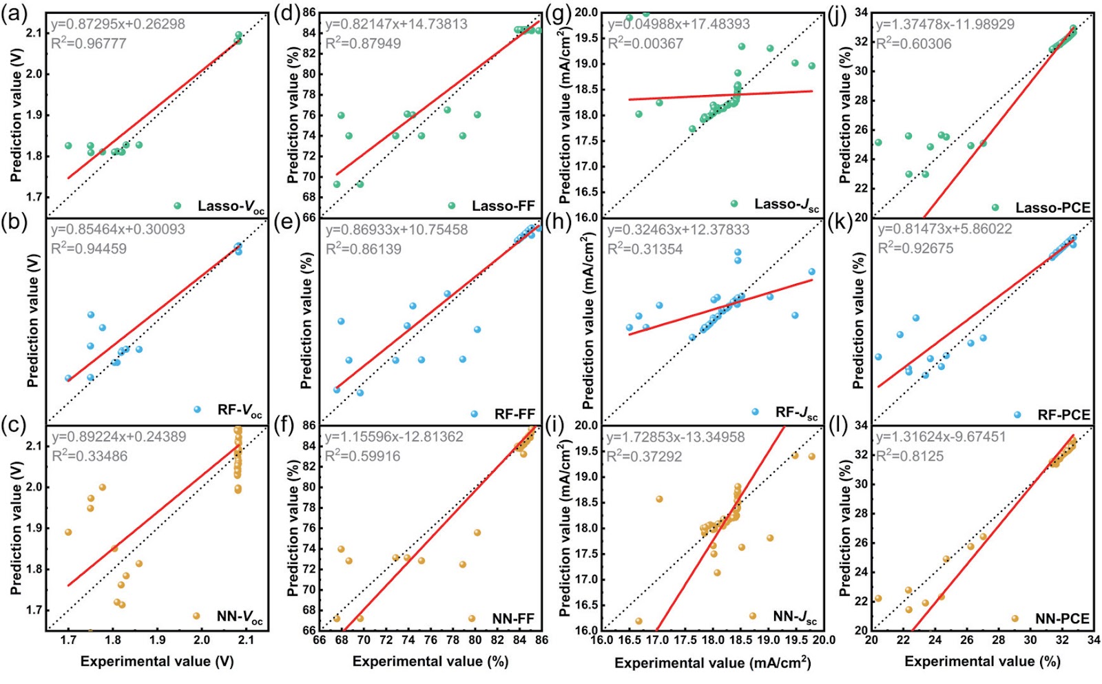
As the development of single-junction solar cells reaches a bottleneck, tandem solar cells have emerged as a critical pathway to further enhance power conversion efficiency. Among them, monolithic perovskite/silicon heterojunction tandem solar cells are currently the fastest-growing technology, achieving the highest efficiencies at relatively low costs. The interconnecting layer, which connects the two sub-cells, plays a crucial role in tandem cell performance. It collects electrons and holes from the respective sub-cells and facilitates recombination and tunneling at the interface. Therefore, the properties of the interconnecting layer are pivotal to the overall device performance. In this work, we applied statistical analysis and machine learning algorithms to systematically analyze the interconnecting layer. A comprehensive dataset on interconnecting layer parameters was established, and predictive modeling was performed using Lasso linear regression, random forest, and multilayer perceptron (a type of neural network). The analysis revealed key feature importance for experimental parameters, providing valuable insights into the application of interconnecting layers in perovskite/silicon heterojunction tandem solar cells. The final optimized interconnecting layer can achieve a proof-of-concept efficiency of 38.17%, providing guidance and direction for the development of monolithic perovskite/silicon tandem solar cells.

Machine learning facilitates the development of interconnecting layers for perovskite/silicon heterojunction tandem solar cells with proof-of-concept efficiency > 38%
Graphical Abstract