SinoTechIntel Academic Portal
🏛️ Indexed Academic JournalImpact Factor: 3.8

Journal of Semiconductors (半导体学报 - 中国科学院半导体研究所)

Authoritative peer-reviewed journal in materials science, metallurgy, chemistry and engineering technologies: Journal of Semiconductors (半导体学报 - Viện Bán dẫn CAS)

Total Research Papers: 115
Access: 100% Free Open Access
Browse by Publication Year & VolumeReset All Filters ✕

Published Research PapersFiltered: Year 2025 • Vol. 32 • 1

Showing 13 of 115 peer-reviewed papers with full Graphical Abstracts.

Original ResearchVol. 32, Issue 1 • pp. 100-112DOI: 10.1088/1674-4926/25010031Jan 15, 2025

Improving electrical performance and fringe effect in p-type SnOx thin film transistors via Ta incorporation

Authors: Yu Song, Runtong Guo, Ruohao Hong, Rui He, Xuming Zou, Benjamin Iñiguez, Denis Flandre, Lei Liao, and Guoli Li

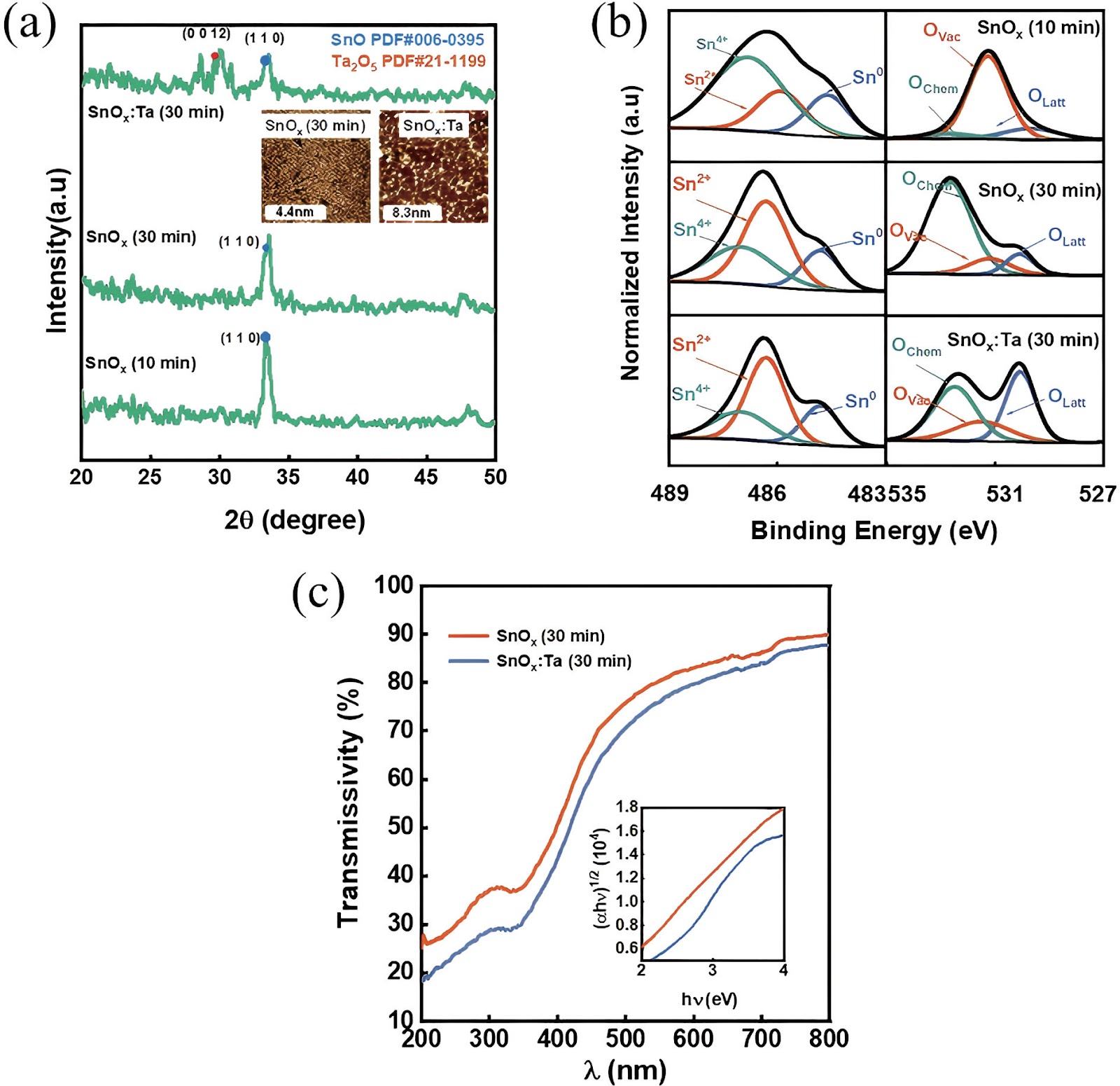
In this work, the incorporation of tantalum (Ta) into p-type metal-oxide (SnOx) semiconductor film is investigated to improve the electrical characteristics and suppress the fringe effect of thin film transistors (TFTs). The Ta-doped SnOx (SnOx:Ta) film is deposited by radio-frequency (RF) magnetron sputtering with a Sn:Ta (3 at.%) target and thermally annealed at 270 °C for 30 min. Here, we observe that the SnOx:Ta film presents increased crystallinity, reduced defect density (3.25 × 1012 cm−2·eV−1), and widened bandgap (1.98 eV), in comparison with the undoped SnOx film. As a result, the SnOx:Ta TFTs exhibit a lower off-state current (Ioff), an improved on/off current ratio (2.17 × 10⁴), a remarkably decreased subthreshold swing (SS) by 41%, and enhanced device stability. Additionally, by introducing Ta dopants, the fringe effect as well as the impact of channel width-to-length ratio (W/L) on electrical performances of the p-type oxide TFTs can be effectively suppressed. These results shall contribute to further exploration and development of p-type SnOx TFTs.
Improving electrical performance and fringe effect in p-type SnOx thin film transistors via Ta incorporation
Graphical Abstract
Original ResearchVol. 32, Issue 1 • pp. 100-112DOI: 10.1088/1674-4926/25010024Jan 15, 2025

AlGaN/GaN-based SBDs grown on silicon substrates with trenched n+-GaN cap layer and local passivation layer to improve BFOM and dynamic properties

Authors: Zhizhong Wang, Jingting He, Fuping Huang, Xuchen Gao, Kangkai Tian, Chunshuang Chu, Yonghui Zhang, Shuting Cai, Xiaojuan Sun, Dabing Li, Xiao Wei Sun, Zi-Hui Zhang

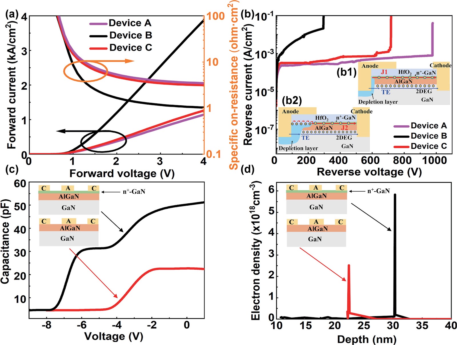
In this work, we design and fabricate AlGaN/GaN-based Schottky barrier diodes (SBDs) on a silicon substrate with a trenched n+-GaN cap layer. With the developed physical models, we find that the n+-GaN cap layer provides more electrons into the AlGaN/GaN channel, which is further confirmed experimentally. When compared with the reference device, this increases the two-dimensional electron gas (2DEG) density by two times and leads to a reduced specific ON-resistance (Ron,sp) of ~2.4 mΩ·cm2. We also adopt the trenched n+-GaN structure such that partial of the n+-GaN is removed by using dry etching process to eliminate the surface electrical conduction when the device is set in the off-state. To suppress the surface defects that are caused by the dry etching process, we also deposit Si3N4 layer prior to the deposition of field plate (FP), and we obtain a reduced leakage current of ~8 × 10⁻⁵ A·cm−2 and breakdown voltage (BV) of 876 V. The Baliga’s figure of merit (BFOM) for the proposed structure is increased to ~319 MW·cm−2. Our investigations also find that the pre-deposited Si3N4 layer helps suppress the electron capture and transport processes, which enables the reduced dynamic Ron,sp.

AlGaN/GaN-based SBDs grown on silicon substrates with trenched n+-GaN cap layer and local passivation layer to improve BFOM and dynamic properties
Graphical Abstract
Original ResearchVol. 32, Issue 1 • pp. 100-112DOI: 10.1088/1674-4926/25010026Jan 15, 2025

Reducing specific contact resistivity of V/Al/Ti/Au n-electrode on n-AlGaN with Al content over 80% for far-UVC LEDs

Authors: Jiale Peng, Ke Jiang, Shanli Zhang, Jianwei Ben, Kexi Liu, Ziyue Qin, Ruihua Chen, Chunyue Zhang, Shunpeng Lv, Xiaojuan Sun, Dabing Li

AlGaN-based LEDs with peak wavelength below 240 nm (far-UVC) pose no significant harm to human health, thus highlighting their broader application potential. While, there is a significant Schottky barrier between the n-electrode and Al-rich n-AlGaN, adversely impeding electron injection and resulting in considerable heat generation. Here, we fabricate V-based electrodes of V/Al/Ti/Au on n-AlGaN with Al content over 80% and investigate the relationship between the metal diffusion and contact properties during the high-temperature annealing process. Experiments reveal that decreasing V thickness in the electrode promotes the diffusion of Al towards the surface of n-AlGaN, which facilitates the formation of VN and thus the increase of local electron concentration, resulting in lower specific contact resistivity. Then, increasing the Al thickness inhibits the diffusion of Au to the n-AlGaN surface, suppressing the rise of Schottky barrier. Experimentally, an optimized n-electrode of V(10 nm)/Al(240 nm)/Ti(40 nm)/Au(50 nm) on n-Al0.81Ga0.19N is obtained, realizing an optimal specific contact resistivity of 7.30 × 10⁻⁴ Ω·cm2. Based on the optimal n-electrode preparation scheme for Al-rich n-AlGaN, the work voltage of a far-UVC LED with peak wavelength of 233.5 nm is effectively reduced.

Reducing specific contact resistivity of V/Al/Ti/Au n-electrode on n-AlGaN with Al content over 80% for far-UVC LEDs
Graphical Abstract
Original ResearchVol. 32, Issue 1 • pp. 100-112DOI: 10.1088/1674-4926/25010015Jan 15, 2025

Review on three-dimensional graphene: synthesis and joint photoelectric regulation in photodetectors

Authors: Bingkun Wang, Jinqiu Zhang, Huijuan Wu, Fanghao Zhu, Shanshui Lian, Genqiang Cao, Hui Ma, Xurui Hu, Li Zheng, Gang Wang

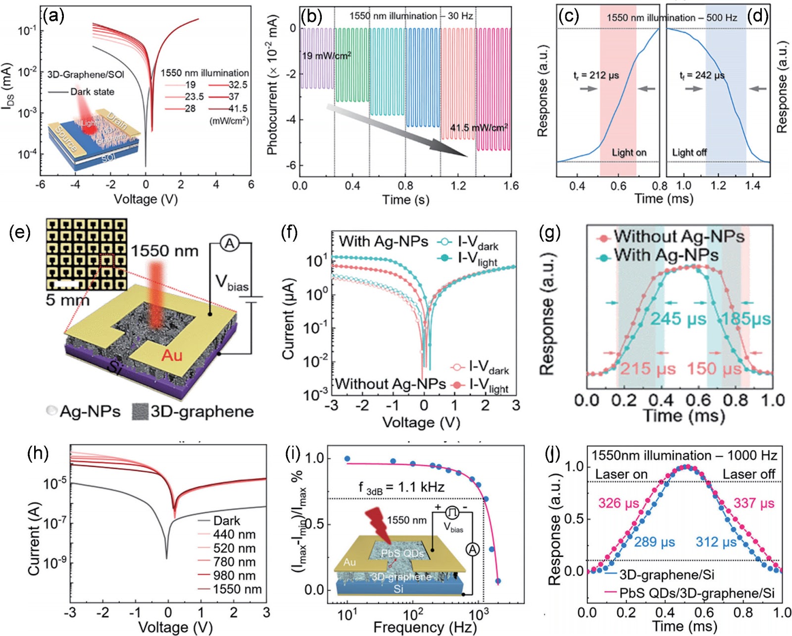
Graphene has garnered significant attention in photodetection due to its exceptional optical, electrical, mechanical, and thermal properties. However, the practical application of two-dimensional (2D) graphene in optoelectronic fields is limited by its weak light absorption (only 2.3%) and zero bandgap characteristics. Increasing light absorption is a critical scientific challenge for developing high-performance graphene-based photodetectors. Three-dimensional (3D) graphene comprises vertically grown stacked 2D-graphene layers and features a distinctive porous structure. Unlike 2D-graphene, 3D-graphene offers a larger specific surface area, improved electrochemical activity, and high chemical stability, making it a promising material for optoelectronic detection. Importantly, 3D-graphene has an optical microcavity structure that enhances light absorption through interaction with incoming light. This paper systematically reviews and analyzes the current research status and challenges of 3D-graphene-based photodetectors, aiming to explore feasible development paths for these devices and promote their industrial application.

Review on three-dimensional graphene: synthesis and joint photoelectric regulation in photodetectors
Graphical Abstract
Original ResearchVol. 32, Issue 1 • pp. 100-112DOI: 10.1088/1674-4926/25010027Jan 15, 2025

Investigating the doping performance of an ionic dopant for organic semiconductors and thermoelectric applications

Authors: Jing Guo, Yaru Feng, Jinjun Zhang, Jing Zhang, Ping-An Chen, Huan Wei, Xincan Qiu, Yu Liu, Jiangnan Xia, Huajie Chen, Yugang Bai, Lang Jiang, Yuanyuan Hu

Doping plays a pivotal role in enhancing the performance of organic semiconductors (OSCs) for advanced optoelectronic and thermoelectric applications. In this study, we systematically investigated the doping performance and applicability of the ionic dopant 4-isopropyl-4′-methyldiphenyliodonium tetrakis(penta-fluorophenyl-borate) (DPI-TPFB) as a p-dopant for OSCs. Using the p-type OSC PBBT-2T as a model system, we demonstrated that DPI-TPFB shows significant doping effect, as confirmed by ESR spectra, ultraviolet−visible−near-infrared (UV−vis−NIR) absorption, and work function analysis, and enhances the electronic conductivity of PBBT-2T films by over four orders of magnitude. Furthermore, DPI-TPFB exhibited broad doping applicability, effectively doping various p-type OSCs and even imparting p-type characteristics to the n-type OSC N2200, transforming its intrinsic n-type behavior into p-type. The application of DPI-TPFB-doped PBBT-2T films in organic thermoelectric devices (OTEs) was also explored, achieving a power factor of approximately 10 μW∙m−1∙K−2. These findings highlight the potential of DPI-TPFB as a versatile and efficient dopant for integration into organic optoelectronic and thermoelectric devices.

Investigating the doping performance of an ionic dopant for organic semiconductors and thermoelectric applications
Graphical Abstract
Original ResearchVol. 32, Issue 1 • pp. 100-112DOI: 10.1088/1674-4926/25010005Jan 15, 2025

4H-SiC superjunction MOSFET with integrated high-K gate dielectric and split gate

Authors: Jiafei Yao, Zhengfei Yang, Yuxuan Dai, Ziwei Hu, Man Li, Kemeng Yang, Jing Chen, Maolin Zhang, Jun Zhang, Yufeng Guo

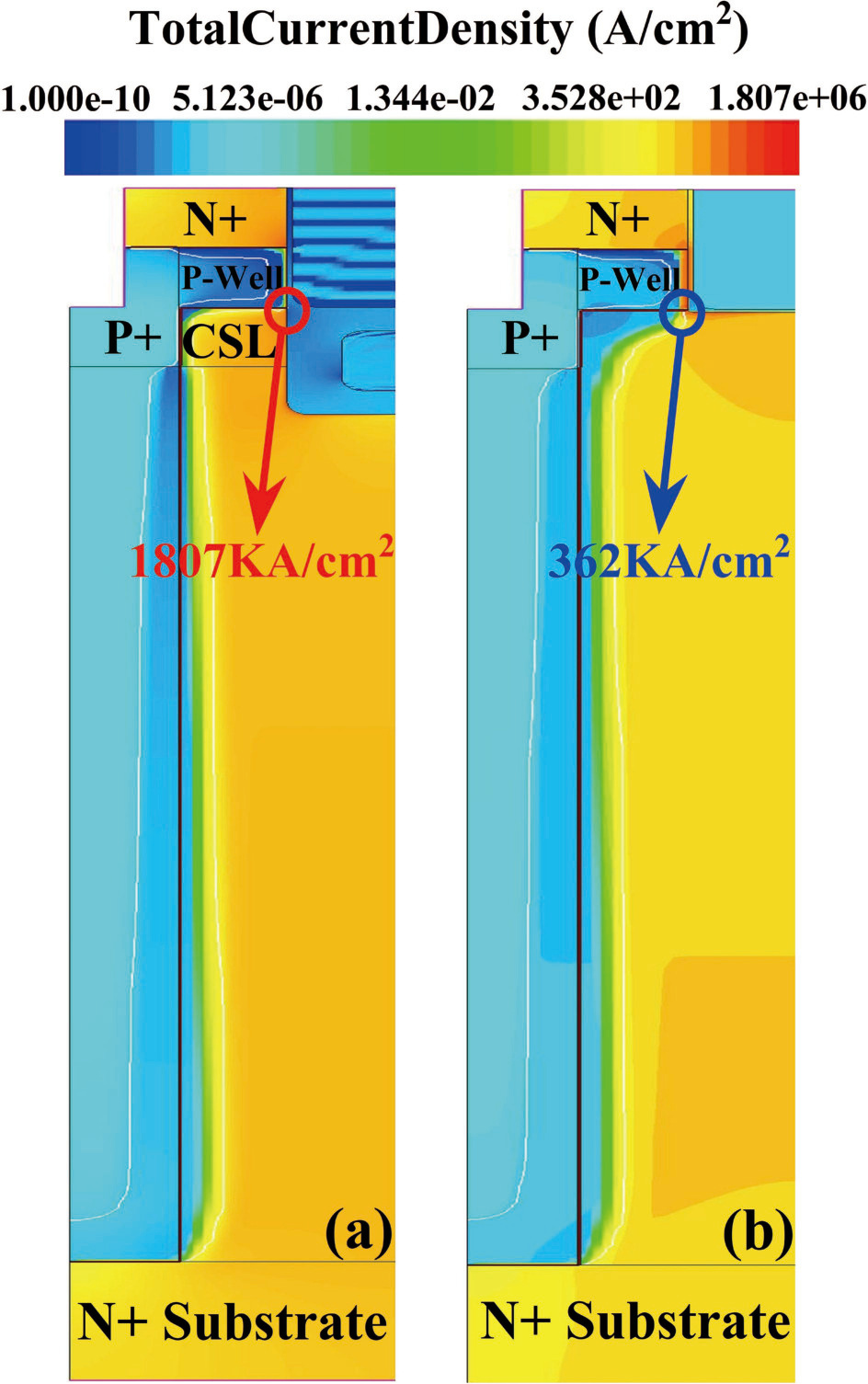
A 4H-SiC superjunction (SJ) MOSFET (SJMOS) with integrated high-K gate dielectric and split gate (HKSG-SJMOS) is proposed in this paper. The key features of HKSG-SJMOS involve the utilization of high-K (HK) dielectric as the gate dielectric, which surrounds the source-connected split gate (SG) and metal gate. The high-K gate dielectric optimizes the electric field distribution within the drift region, creating a low-resistance conductive channel. This enhancement leads to an increase in the breakdown voltage (BV) and a reduction in the specific on resistance (Ron,sp). The introduction of split gate surrounded by high-K dielectric reduces the gate−drain capacitance (Cgd) and gate−drain charge (Qgd), which improves the switching characteristics. The simulation results indicate that compared to conventional 4H-SiC SJMOS, the HKSG-SJMOS exhibits a 110.5% enhancement in figure of merit (FOM, FOM = BV2/Ron,sp), a 93.6% reduction in the high frequency figure of merit (HFFOM) of Ron,sp·Cgd, and reductions in turn-on loss (Eon) and turn-off loss (Eoff) by 38.3% and 31.6%, respectively. Furthermore, the reverse recovery characteristics of HKSG-SJMOS has also discussed, revealing superior performance compared to conventional 4H-SiC SJMOS.

4H-SiC superjunction MOSFET with integrated high-K gate dielectric and split gate
Graphical Abstract
Original ResearchVol. 32, Issue 1 • pp. 100-112DOI: 10.1088/1674-4926/25010030Jan 15, 2025

A 2D/3D vision chip based on organic substrate 3D package

Authors: Siyuan Wei, Quanmin Chen, Jingyi Yu, Xuanzhe Xu, Yuxiao Wen, Runjiang Dou, Shuangming Yu, Guike Li, Kaiming Nie, Jie Cheng, Jiangtao Xu, Liyuan Liu, Nanjian Wu

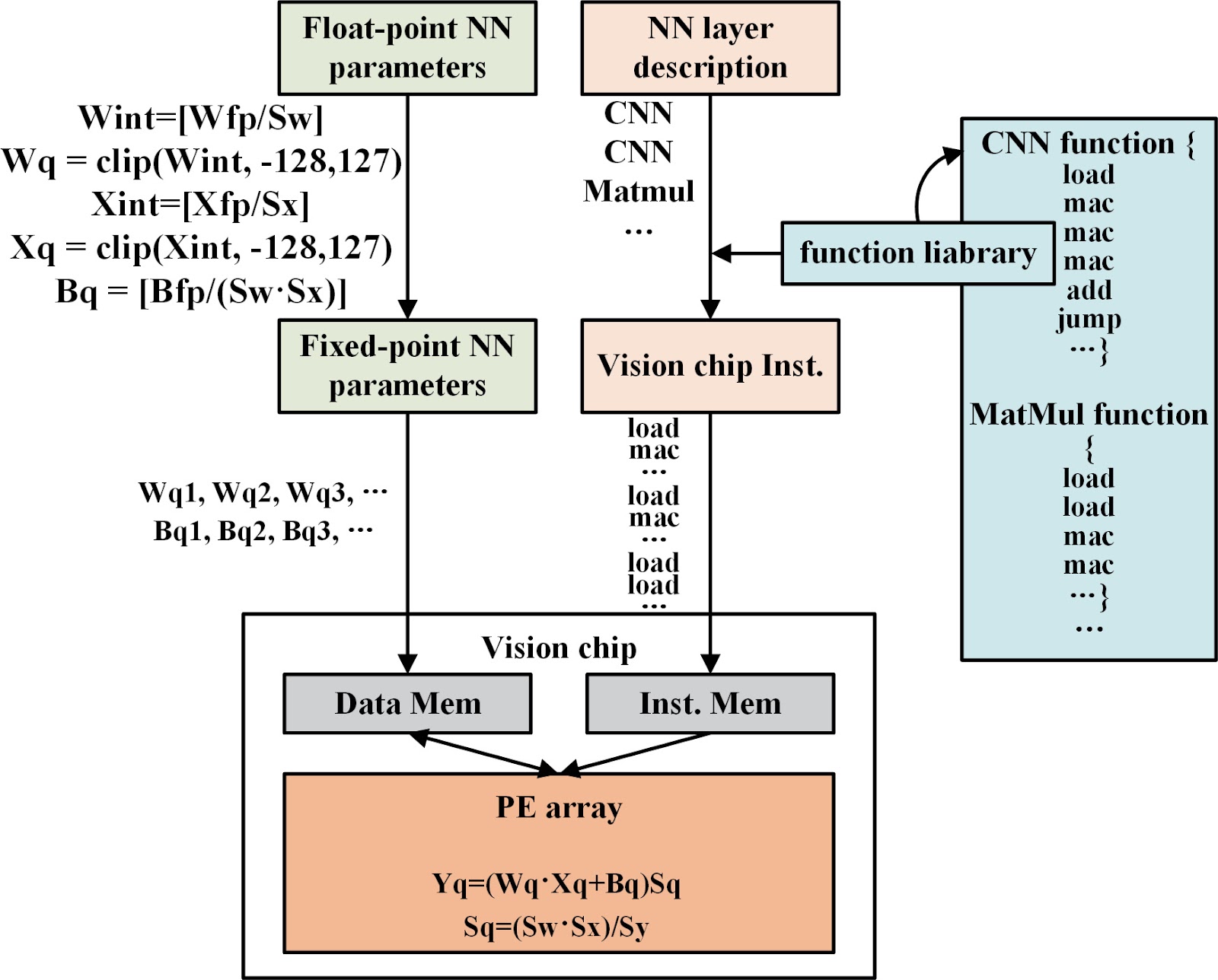
This paper describes a 2D/3D vision chip with integrated sensing and processing capabilities. The 2D/3D vision chip architecture includes a 2D/3D image sensor and a programmable visual processor. In this architecture, we design a novel on-chip processing flow with die-to-die image transmission and low-latency fixed-point image processing. The vision chip achieves real-time end-to-end processing of convolutional neural networks (CNNs) and conventional image processing algorithms. Furthermore, an end-to-end 2D/3D vision system is built to exhibit the capacity of the vision chip. The vision system achieves real-timing applications under 2D and 3D scenes, such as human face detection (processing delay 10.2 ms) and depth map reconstruction (processing delay 4.1 ms). The frame rate of image acquisition, image process, and result display is larger than 30 fps.

A 2D/3D vision chip based on organic substrate 3D package
Graphical Abstract
Original ResearchVol. 32, Issue 1 • pp. 100-112DOI: 10.1088/1674-4926/25010010Jan 15, 2025

Topological materials-based photodetectors from the infrared to terahertz range

Authors: Zhaowen Bao, Yiming Wang, Kaixuan Zhang, Yingdong Wei, Xiaokai Pan, Zhen Hu, Shiqi Lan, Yichong Zhang, Xiaoyun Wang, Huichuan Fan, Hongfei Wu, Lei Yang, Zhiyuan Zhou, Xin Sun, Yulu Chen, Lin Wang

Infrared and terahertz waves constitute pivotal bands within the electromagnetic spectrum, distinguished by their robust penetration capabilities and non-ionizing nature. These wavebands offer the potential for achieving high-resolution and non-destructive detection methodologies, thereby possessing considerable research significance across diverse domains including communication technologies, biomedical applications, and security screening systems. Two-dimensional materials, owing to their distinctive optoelectronic attributes, have found widespread application in photodetection endeavors. Nonetheless, their efficacy diminishes when tasked with detecting lower photon energies. Furthermore, as the landscape of device integration evolves, two-dimensional materials struggle to align with the stringent demands for device superior performance. Topological materials, with their topologically protected electronic states and non-trivial topological invariants, exhibit quantum anomalous Hall effects and ultra-high carrier mobility, providing a new approach for seeking photosensitive materials for infrared and terahertz photodetectors. This article introduces various types of topological materials and their properties, followed by an explanation of the detection mechanism and performance parameters of photodetectors. Finally, it summarizes the current research status of near-infrared to far-infrared photodetectors and terahertz photodetectors based on topological materials, discussing the challenges faced and future prospects in their development.

Topological materials-based photodetectors from the infrared to terahertz range
Graphical Abstract
Original ResearchVol. 32, Issue 1 • pp. 100-112DOI: 10.1088/1674-4926/25010002Jan 15, 2025

A K/Ka-band series Doherty CMOS power amplifier with distributed multi-step impedance inverting network

Authors: Xinyu Jiang, Wei Deng, Junlong Gong, Haikun Jia, Baoyong Chi

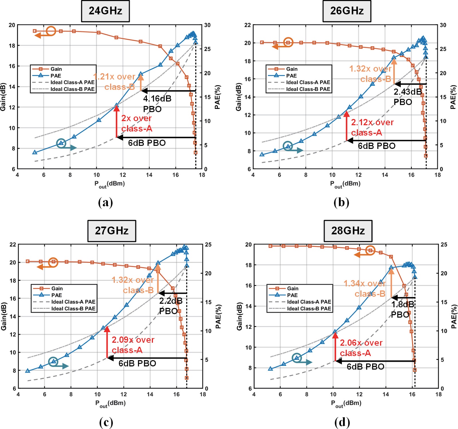
A two-way K/Ka-band series-Doherty PA (SDPA) with a distributed impedance inverting network (IIN) for millimeter wave applications is presented in this article. The proposed distributed IIN contributes to achieve wideband linear and power back-off (PBO) efficiency enhancement. Implemented in 65 nm bulk CMOS technology, this work realizes a measured 3 dB bandwidth of 15.5 GHz with 21.2 dB peak small-signal gain at 34.2 GHz. Under 1-V power supply, it achieves OP1dB over 13.4 dBm and Psat over 16 dBm between 21 to 30 GHz. The measured maximum Psat, OP1dB, peak/OP1dB/6dBPBO PAE results are 17.5, 14.7 dBm, and 28.2%/23.2%/13.2%. Without digital pre-distortion (DPD) and equalization, EVMs are lower than −25.2 dB for 200 MHz 64-QAM signals. Besides, this work achieves −33.35, −23.52, and −20 dB EVMs for 100 MHz 256-QAM, 600 MHz 64-QAM and 2 GHz 16-QAM signals at 27 GHz without DPD and equalization.

A K/Ka-band series Doherty CMOS power amplifier with distributed multi-step impedance inverting network
Graphical Abstract
Original ResearchVol. 32, Issue 1 • pp. 100-112DOI: 10.1088/1674-4926/25010028Jan 15, 2025

A battery-free wireless temperature sensing chipset implemented by 55 and 65 nm CMOS process

Authors: Jiayi Wang, Haoyang Li, Weixiao Wang, Tianying Fang, Jiaqing Li, Yuxuan Luo, Bo Zhao

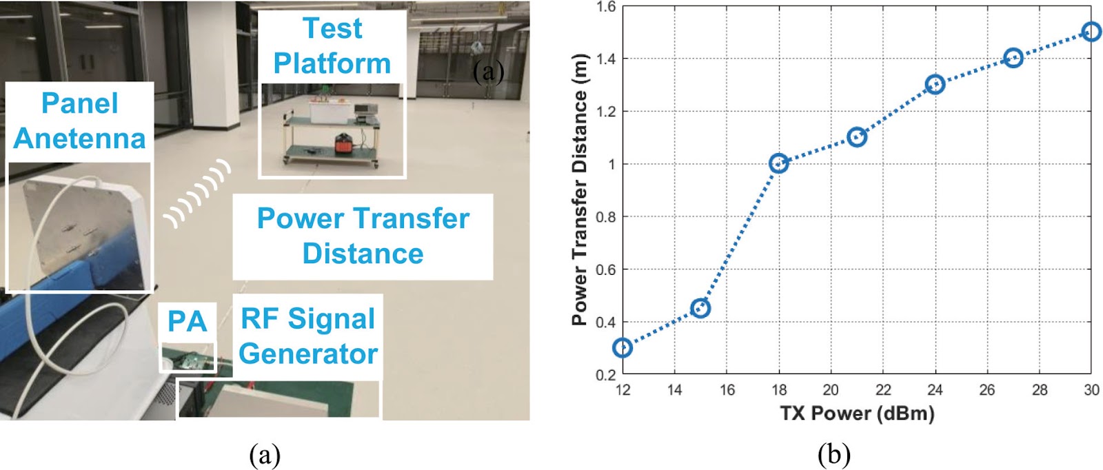
In the applications such as food production, the environmental temperature should be measured continuously during the entire process, which requires an ultra-low-power temperature sensor for long-termly monitoring. Conventional temperature sensors trade the measurement accuracy with power consumption. In this work, we present a battery-free wireless temperature sensing chip for long-termly monitoring during food production. A calibrated oscillator-based CMOS temperature sensor is proposed instead of the ADC-based power-hungry circuits in conventional works. In addition, the sensor chip can harvest the power transferred by a remote reader to eliminate the use of battery. Meanwhile, the system conducts wireless bidirectional communication between the sensor chip and reader. In this way, the temperature sensor can realize both a high precision and battery-free operation. The temperature sensing chip is fabricated in 55 nm CMOS process, and the reader chip is implemented in 65 nm CMOS technology. Experimental results show that the temperature measurement error achieves ±1.6 °C from 25 to 50 °C, with battery-free readout by a remote reader.

A battery-free wireless temperature sensing chipset implemented by 55 and 65 nm CMOS process
Graphical Abstract
Original ResearchVol. 32, Issue 1 • pp. 100-112DOI: 10.1088/1674-4926/25010017Jan 15, 2025

Growth and optical properties of large-sized Co2+: ZnGa2O4 single crystal

Authors: Zhengyuan Li, Jiaqi Wei, Yiyuan Liu, Huihui Li, Yang Li, Zhitai Jia, Xutang Tao, Wenxiang Mu

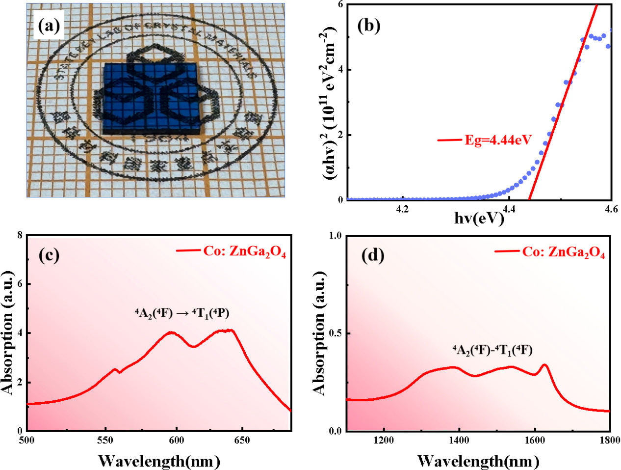
The transition of cobalt ions located at tetrahedral sites will produce strong absorption in the visible and near-infrared regions, and is expected to work in a passively Q-switched solid-state laser at the eye-safe wavelength of 1.5 µm. In this study, Co2+ ions were introduced into the wide bandgap semiconductor material ZnGa2O4, and large-sized and high-quality Co2+-doped ZnGa2O4 crystals with a volume of about 20 cm3 were grown using the vertical gradient freeze (VGF) method. Crystal structure and optical properties were analyzed using X-ray powder diffraction (XRD), X-ray photoelectron spectroscopy (XPS), and absorption spectroscopy. XRD results show that the Co2+-doped ZnGa2O4 crystal has a pure spinel phase without impurity phases and the rocking curve full width at half maximum (FWHM) is only 58 arcsec. The concentration of Co2+ in Co2+-doped ZnGa2O4 crystals was determined to be 0.2 at.% by the energy dispersive X-ray spectroscopy. The optical band gap of Co2+-doped ZnGa2O4 crystals is 4.44 eV. The optical absorption spectrum for Co2+-doped ZnGa2O4 reveals a prominent visible absorption band within 550−670 nm and a wide absorption band spanning from 1100 to 1700 nm. This suggests that the Co2+ ions have substituted the Zn2+ ions, which are typically tetrahedrally coordinated, within the lattice structure of ZnGa2O4. The visible region's absorption peak and the near-infrared broad absorption band are ascribed to the 4A2(4F) → 4T1(4P) and 4A2(4F) →4T1(4F) transitions, respectively. The optimal ground state absorption cross section was determined to be 3.07 × 10⁻¹⁹ cm2 in ZnGa2O4, a value that is comparatively large within the context of similar materials. This finding suggests that ZnGa2O4 is a promising candidate for use in near-infrared passive Q-switched solid-state lasers.

Growth and optical properties of large-sized Co2+: ZnGa2O4 single crystal
Graphical Abstract
Original ResearchVol. 32, Issue 1 • pp. 100-112DOI: 10.1088/1674-4926/25010022Jan 15, 2025

Research on heterojunction semiconductor photodetectors based on CsPbBr3 QDs/CsPbBrxI3–x QDs

Authors: Chenguang Shen, Mengwei Chen, Wei Huang, Yingping Yang

All-inorganic CsPbBr3 perovskite quantum dots (QDs) have attracted extensive attention in photoelectric detection for their excellent photoelectric properties and stability. However, the CsPbBr3 quantum dot film exhibits a high non-radiative recombination rate, and the mismatch in energy levels with the carbon electrode weakens hole extraction efficiency. These reduces the device's performance. To improve this, a semiconductor photodetector based on fluorine-doped tin oxide (FTO)/dense titanium dioxide (c-TiO2)/mesoporous titanium dioxide (m-TiO2)/CsPbBr3 QDs/CsPbBrxI3–x (x = 2, 1.5, 1) QDs/C structure was studied. By adjusting the Br– : I– ratio, the synthesized CsPbBrxI3–x (x = 2, 1.5, 1) QDs showed an adjustable band gap width of 2.284−2.394 eV. And forming a type Ⅱ band structure with CsPbBr3 QDs, which reduced the valence band offset between the active layer and the carbon electrode, this promoted carrier extraction and reduced non-radiative recombination rate. Compared with the original device (the photosensitive layer is CsPbBr3 QDs), the performance of the photodetector based on the CsPbBr3 QDs/CsPbBr2I QDs heterostructure is significantly improved, the responsivity (R) increased by 73%, the specific detectivity rate (D*) increased from 6.98 × 10¹² to 3.19 × 10¹³ Jones, the on/off ratio reached 106. This study provides a new idea for the development of semiconductor tandem detectors.

Research on heterojunction semiconductor photodetectors based on CsPbBr3 QDs/CsPbBrxI3–x QDs
Graphical Abstract
Original ResearchVol. 32, Issue 1 • pp. 100-112DOI: 10.1088/1674-4926/25010021Jan 15, 2025

Interface energetics in organic and perovskite semiconductor solar cells

Authors: Shaobing Xiong, Mats Fahlman, Qinye Bao

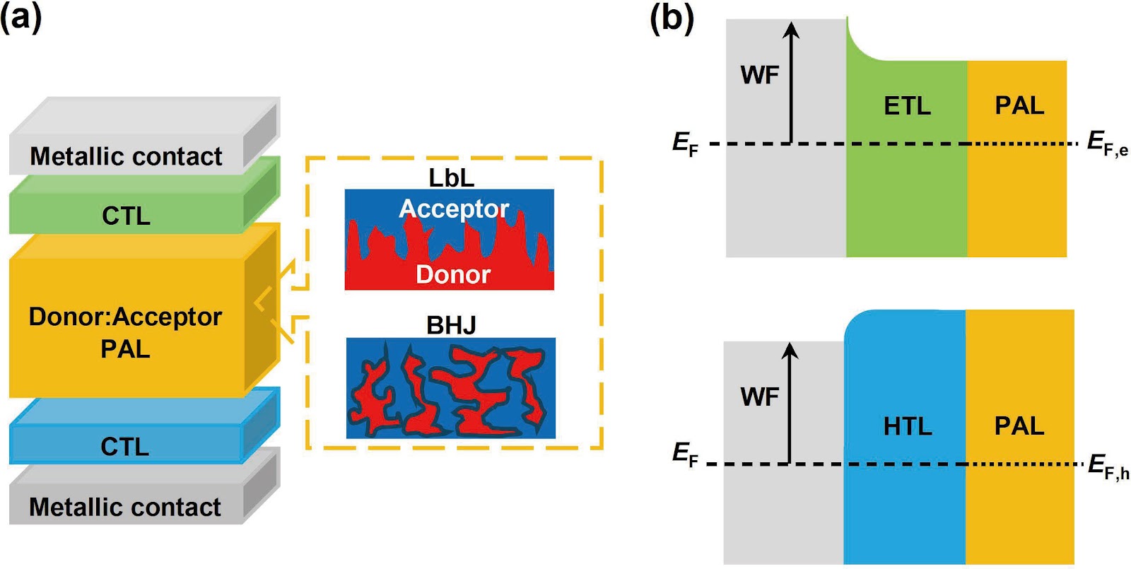
Improving the quality of life for Earth’s growing population is a complex task that requires the development of new technologies and materials. Perhaps the biggest challenge is access to clean and renewable energy sources that can drive a sustainable future. Photovoltaics, today mainly represented by silicon-based solar cells, convert solar energy into electricity and is already an important component in the renewable energy portfolio. Organic solar cells (OSCs) and perovskite solar cells (PSCs) both offer advantages compared to silicon solar cells such as low-temperature solution processing, flexibility and semi-transparency while sharing similar device structures consisting of a photoactive layer (PAL) sandwiched between an anode and a cathode contact. The anode and cathode contacts in OSCs and PSCs typically consist of a charge transport layer (CTL) and a conductor (often a metal), and the CTLs significantly impact device performance. The CTLs used in OSCs and PSCs share many functionalities. OSCs and PSCs fabrication involves sequential deposition of layers from solution and treatments at elevated temperatures, so the CTLs must be solvent resistant and stable under thermal cycling (also important for long-term device stability). Preferably, the CTLs should also have sufficient tolerance to thickness variations to facilitate roll-to-roll fabrication. The CTL requirements however differ for OSCs and PSCs due to the unique respective properties of the organic semiconductor and metal halide perovskite PALs, so we will discuss them separately below.

Interface energetics in organic and perovskite semiconductor solar cells
Graphical Abstract