SinoTechIntel Academic Portal
🏛️ Indexed Academic JournalImpact Factor: 3.8

Journal of Semiconductors (半导体学报 - 中国科学院半导体研究所)

Authoritative peer-reviewed journal in materials science, metallurgy, chemistry and engineering technologies: Journal of Semiconductors (半导体学报 - Viện Bán dẫn CAS)

Total Research Papers: 115
Access: 100% Free Open Access
Browse by Publication Year & VolumeReset All Filters ✕

Published Research PapersFiltered: Year 2025 • Vol. 32 • 7

Showing 4 of 115 peer-reviewed papers with full Graphical Abstracts.

Original ResearchVol. 32, Issue 7 • pp. 100-112DOI: 10.1088/1674-4926/25070024Jan 15, 2025

Optimization and defect control in photoresist etch back processes for advanced semiconductor technologies

Authors: Ting Lei, Zhehong Liu, Zhiwen Liu, Guangjie Xue, Chun Sun, Jun Zhou, Xiangshui Miao

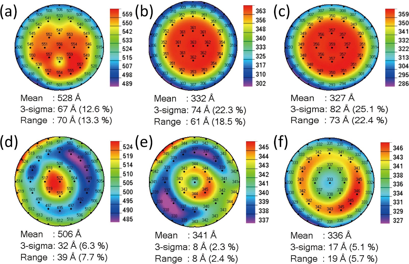
The introduction of high-k/metal gate (HK/MG) technology enables independent tuning of N-type metal−oxide−semiconductor (NMOS) and P-type metal−oxide−semiconductor (PMOS) threshold voltages, facilitating advanced nodes and improving overall chip performance. However, severe pattern loading effects during PMOS device fabrication pose challenges in dummy poly removal. This work reports the optimization of the photoresist etch back (PREB) process, providing a wider process window for subsequent AL CMP. By tuning the PR coating uniformity to 1.6% and applying four-zone electrostatic chuck (ESC) temperature control, the wafer-level uniformities of PR, SiN, and SiO2 were reduced to 6.3%, 2.3%, and 5.1%, respectively. An optimized over etch (OE) recipe with a high selectivity of PR : SiN : SiO2 ≈ 1 : 1 : 6 effectively balanced gate height loading between N- and PMOS regions. Furthermore, precise EB1 time tuning enabled defect removal, while advanced KLA inspection ensured early detection of critical failure modes. Collectively, these measures establish a robust and stable PREB process for advanced logic device fabrication.
Optimization and defect control in photoresist etch back processes for advanced semiconductor technologies
Graphical Abstract
Original ResearchVol. 32, Issue 7 • pp. 100-112DOI: 10.1088/1674-4926/25070023Jan 15, 2025

Harnessing Eu/Ce-codoped ZnO nanomaterial derived from MOF precursor for high-performance n-butanol sensing under UV activation at ambient temperature

Authors: Yinzhong Liu, Xuechun Yang, Yun Guo, Lingchao Wang, Xiaofan Li, Hui Guo, Yiyu Qiao, Xiaotao Zhu, Lingli Cheng, Zheng Jiao

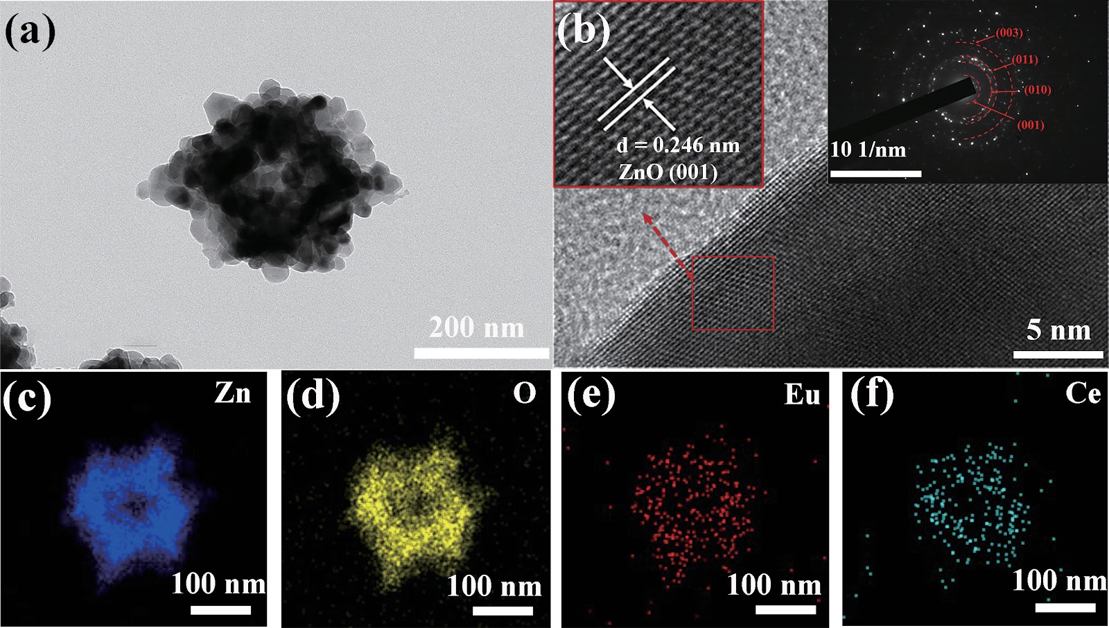
Prolonged exposure to n-butanol, a common hazardous volatile organic compound (VOC) in the environment, can lead to a broad range of adverse health effects. Therefore, detecting n-butanol safely and efficiently at low concentrations becomes critical for both environmental monitoring and human health. In this study, a novel Eu/Ce-codoped MOF-ZnO gas sensor was developed for the sensitive detection of n-butanol gas under ultraviolet activation at ambient temperature. A series of Eu/Ce-ZnO nanomaterials were synthesized via a simple co-precipitation route, by carefully designing the varied mass ratios of Eu and Ce incorporated into pristine ZnO derived from MOF precursors. The gas testing results revealed that introducing an appropriate amount of Eu and Ce would enlarge the specific surface area and enrich the oxygen vacancy content compared to pristine MOF-ZnO. Upon UV irradiation, the 0.03 wt% Eu 0.04 wt% Ce-ZnO sensor achieved a superior response of 611 for 100 ppm n-butanol at room temperature, 15.28 times higher than that of pristine MOF-ZnO (40). Furthermore, the sensor presented rapid response/recovery times (15 s/28 s) and excellent selectivity. The above contributions pave the way for the promising development of highly sensitive, ultraviolet-enhanced gas sensors for ambient temperature detection of VOCs.

Harnessing Eu/Ce-codoped ZnO nanomaterial derived from MOF precursor for high-performance n-butanol sensing under UV activation at ambient temperature
Graphical Abstract
Original ResearchVol. 32, Issue 7 • pp. 100-112DOI: 10.1088/1674-4926/25070031Jan 15, 2025

Room-temperature electrically injected GaN-based photonic-crystal surface-emitting lasers

Authors: Tong Xu, Meixin Feng, Xiujian Sun, Rui Xi, Xinchao Li, Shuming Zhang, Qian Sun, Xiaoqi Yu, Kanglin Xiong, Hui Yang, Xianfei Zhang, Zhuangpeng Guo, Peng Chen

Photonic crystal surface emitting lasers (PCSELs) utilize the Bragg diffraction of two-dimensional photonic crystals to achieve a single-mode output with a high power and a small divergence angle, and has recently attracted much attention. In 2023, Kyoto University reported GaAs-based 945 nm PCSELs with a continuous-wave (CW) single-mode output power of exceeding 50 W, and a narrow beam divergence angle of 0.05°, demonstrating a brightness of 1 GW·cm−2·sr−1, which rivals those of the existing bulky lasers. As compared with GaAs/InP-based materials, the emission wavelength of GaN-based materials is shorter, covering the spectrum from visible light to deep ultraviolet, which brings great promise to GaN-based PCSELs for various important applications, such as material processing, laser illumination, underwater communication, visible light communication, chip-scale atomic clock, laser medical treatment and so on. However, the development of GaN-based PCSELs is hindered by its small refractive index, immature regrowth and device fabrication processing technology. So far, only Kyoto University and Canon Corporation have achieved room-temperature (RT) electrically pumped lasing of GaN-based PCSELs with air holes retained via regrowth approach, which would inevitably degrade the material quality, complicate the fabrication process, and increase manufacturing costs. Compared to the regrowth-based methods, the regrowth-free approach reduces the fabrication complexity while maintaining the device performance, offering a cost-effective solution for mass production. In this letter, we reported regrowth-free GaN-based PCSELs grown on sapphire substrate, and demonstrated the RT electrically pumped lasing of GaN-based PCSELs with a threshold current density of 13.7 kA/cm2.

Room-temperature electrically injected GaN-based photonic-crystal surface-emitting lasers
Graphical Abstract
Original ResearchVol. 32, Issue 7 • pp. 100-112DOI: 10.1088/1674-4926/25070029Jan 15, 2025

Contrastive learning for data-efficient substrate deoxidation monitoring in edge-side adaptive molecular beam epitaxy systems

Authors: Yuehao Li, Chao Shen, Wenkang Zhan, Bo Xu, Yazhou Yang, Xu Zhang, Hongchang Wang, Chao Zhao, Haifang Jian

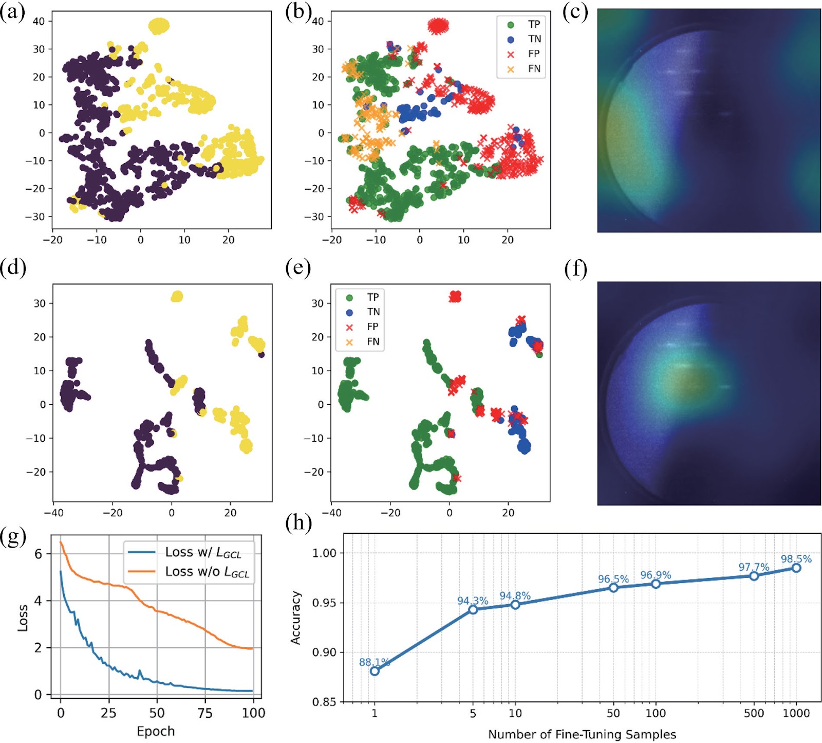
Accurate temperature control and effective oxide removal are essential for achieving high-quality epitaxial growth in molecular beam epitaxy (MBE). However, traditional methods often rely on manual identification of reflection high-energy electron diffraction (RHEED) patterns. This process is heavily influenced by the grower’s experience, leading to issues with reproducibility and limiting the potential for automation. In this report, we propose an unsupervised learning framework for real-time RHEED analysis during the deoxidation process. By incorporating temporal similarity constraints into contrastive learning, our model generates smooth and interpretable feature trajectories that illustrate transitions in the deoxidation state, thus eliminating the need for manual labeling. The model, pre-trained using grouped contrastive loss, shows significant improvement in RHEED feature boundary discrimination and localization of critical regions. We evaluated its generalizability through two transfer learning strategies: calibration-free clustering and few-shot fine-tuning. The pre-trained model achieved a clustering accuracy of 88.1% for GaAs deoxidation samples without additional labels and reached an accuracy of 94.3% to 95.5% after fine-tuning with just five sample pairs across GaAs, Ge, and InAs substrates. This framework is optimized for resource-constrained edge devices, allowing for real-time, plug-and-play integration with existing MBE systems and swift adaptation across various materials and equipment. This work paves the way for greater automation and improved reproducibility in semiconductor manufacturing.

Contrastive learning for data-efficient substrate deoxidation monitoring in edge-side adaptive molecular beam epitaxy systems
Graphical Abstract