SinoTechIntel Academic Portal
🏛️ Indexed Academic JournalImpact Factor: 3.8

Journal of Semiconductors (半导体学报 - 中国科学院半导体研究所)

Authoritative peer-reviewed journal in materials science, metallurgy, chemistry and engineering technologies: Journal of Semiconductors (半导体学报 - Viện Bán dẫn CAS)

Total Research Papers: 115
Access: 100% Free Open Access
Browse by Publication Year & VolumeReset All Filters ✕
Select Specific Issue:

Published Research PapersFiltered: Year 2024 • Vol. 32 • 12

Showing 6 of 115 peer-reviewed papers with full Graphical Abstracts.

Original ResearchVol. 32, Issue 12 • pp. 100-112DOI: 10.1088/1674-4926/24120040Jan 15, 2024

Diverse methods and practical aspects in controlling single semiconductor qubits: a review

Authors: Jia-Ao Peng, Chu-Dan Qiu, Wen-Long Ma, Jun-Wei Luo

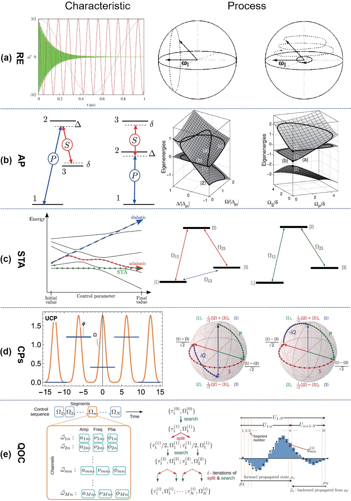
Quantum control allows a wide range of quantum operations employed in molecular physics, nuclear magnetic resonance and quantum information processing. Thanks to the existing microelectronics industry, semiconducting qubits, where quantum information is encoded in spin or charge degree freedom of electrons or nuclei in semiconductor quantum dots, constitute a highly competitive candidate for scalable solid-state quantum technologies. In quantum information processing, advanced control techniques are needed to realize quantum manipulations with both high precision and noise resilience. In this review, we first introduce the basics of various widely-used control methods, including resonant excitation, adabatic passage, shortcuts to adiabaticity, composite pulses, and quantum optimal control. Then we review the practical aspects in applying these methods to realize accurate and robust quantum gates for single semiconductor qubits, such as Loss–DiVincenzo spin qubit, spinglet-triplet qubit, exchange-only qubit and charge qubit.

Diverse methods and practical aspects in controlling single semiconductor qubits: a review
Graphical Abstract
Original ResearchVol. 32, Issue 12 • pp. 100-112DOI: 10.1088/1674-4926/24120034Jan 15, 2024

A 1.25 μW/ch TDM-based analog front-end using a charge-sharing multiplexer for bio-potential recording

Authors: Yifan Huang, Jing Wang, Lin Cheng

This paper presents the design of a low-power multi-channel analog front-end (AFE) for bio-potential recording. By using time division multiplexing (TDM), a successive approximation register analog-to-digital converter (SAR ADC) is shared among all 20 channels. A charge-sharing multiplexer (MUX) is proposed to transmit the output signals from the respective channels to the ADC. By separately pre-sampling the output of each channel, the sampling time of each channel is greatly extended and additional active buffers are avoided. The AFE is fabricated in a 65-nm CMOS process, and the whole system consumes 28.2 μW under 1 V supply. Each analog acquisition channel consumes 1.25 μW and occupies a chip area of 0.14 mm2. Measurement results show that the AFE achieves an input referred noise of 1.8 μV∙rms in a 350 Hz bandwidth and a noise efficiency factor (NEF) of 4.1. The 12-bit SAR ADC achieves an ENOB of 9.8 bit operating at 25 kS/s. The AFE is experimented on real-world applications by measuring human ECG and a clear ECG waveform is captured.

A 1.25 μW/ch TDM-based analog front-end using a charge-sharing multiplexer for bio-potential recording
Graphical Abstract
Original ResearchVol. 32, Issue 12 • pp. 100-112DOI: 10.1088/1674-4926/24120026Jan 15, 2024

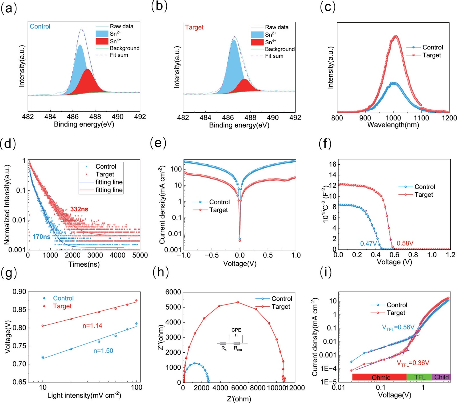
Minimizing tin (Ⅱ) oxidation using ethylhydrazine oxalate for high-performance all-perovskite tandem solar cells

Authors: Jianhua Zhang, Xufeng Liao, Weisheng Li, Yutian Tian, Qinyang Huang, Yitong Ji, Guotang Hu, Qingguo Du, Wenchao Huang, Donghoe Kim, Yi-Bing Cheng, Jinhui Tong

All-perovskite tandem solar cells (ATSCs) have the potential to surpass the Shockley−Queisser efficiency limit of conventional single-junction devices. However, the performance and stability of mixed tin–lead (Sn–Pb) perovskite solar cells (PSCs), which are crucial components of ATSCs, are much lower than those of lead-based perovskites. The primary challenges include the high crystallization rate of perovskite materials and the susceptibility of Sn2+ oxidation, which leads to rough morphology and unfavorable p-type self-doping. To address these issues, we introduced ethylhydrazine oxalate (EDO) at the perovskite interface, which effectively inhibits the oxidation of Sn2+ and simultaneously enhances the crystallinity of the perovskite. Consequently, the EDO-modified mixed tin−lead PSCs reached a power conversion efficiency (PCE) of 21.96% with high reproducibility. We further achieved a 27.58% efficient ATSCs by using EDO as interfacial passivator in the Sn−Pb PSCs.

Minimizing tin (Ⅱ) oxidation using ethylhydrazine oxalate for high-performance all-perovskite tandem solar cells
Graphical Abstract
Original ResearchVol. 32, Issue 12 • pp. 100-112DOI: 10.1088/1674-4926/24120014Jan 15, 2024

Mid-wavelength infrared planar junction photodetector based on InAs/GaSb Type-Ⅱ superlattices

Authors: ZHANG Shihao, HAO Hongyue, ZHANG Ye, WANG Shuo, ZHANG Xiangyu, XIE Ruoyu, YAO Lingze, CHANG Faran, SHAN Yifan, LIU Haofeng, WANG Guowei, WU Donghai, JIANG Dongwei, XU Yingqiang, NIU Zhichuan, DONG Wenjing

In this paper, a planar junction mid-wavelength infrared (MWIR) photodetector based on an InAs/GaSb type-Ⅱ superlattices (T2SLs) is reported. The Intrinsic-πMN superlattices was grown by the molecular beam epitaxy (MBE), followed with a ZnS layer grown by the chemical vapor deposition (CVD). The p-type contact layer was constructed by thermal diffusion in the undoped superlattices. The Zinc atom was successfully realised into the superlattice and a PπMN T2SL structure was constructed. Furthermore, the effects of different diffusion temperatures on the dark current performance of the devices were researched. The 50% cut-off wavelength of the photodetector is 5.26 μm at 77 K with 0 V bias. The minimum dark current density is 8.67 × 10⁻⁵ A/cm2 and the maximum quantum efficiency of 42.5%, and the maximum detectivity reaches 3.90 × 1010 cm·Hz1/2/W at 77 K. The 640 × 512 focal plane arrays (FPA) based on the planner junction were fabricated afterwards. The FPA achieves a noise equivalent temperature difference (NETD) of 539 mK.

Mid-wavelength infrared planar junction photodetector based on InAs/GaSb Type-Ⅱ superlattices
Graphical Abstract
Original ResearchVol. 32, Issue 12 • pp. 100-112DOI: 10.1088/1674-4926/24120018Jan 15, 2024

Size matters: quantum confinement-driven dynamics in CsPbI3 quantum dot light-emitting diodes

Authors: LI Shuo, YIN Wenxu, ZHENG Weitao, ZHANG Xiaoyu

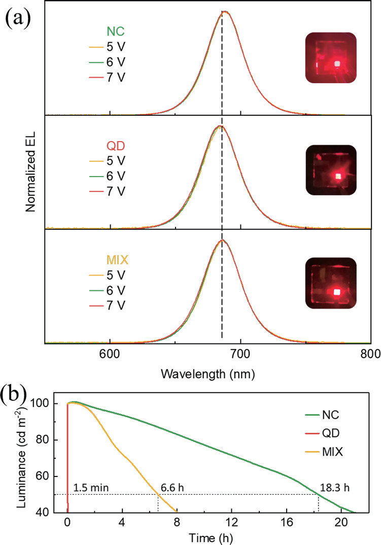
The quantum confinement effect fundamentally alters the optical and electronic properties of quantum dots (QDs), making them versatile building blocks for next-generation light-emitting diodes (LEDs). This study investigates how quantum confinement governs the charge transport, exciton dynamics, and emission efficiency in QD-LEDs, using CsPbI3 QDs as a model system. By systematically varying QD sizes, we reveal size-dependent trade-offs in LED performance, such as enhanced efficiency for smaller QDs but increased brightness and stability for larger QDs under high current densities. Our findings offer critical insights into the design of high-performance QD-LEDs, paving the way for scalable and energy-efficient optoelectronic devices.

Size matters: quantum confinement-driven dynamics in CsPbI3 quantum dot light-emitting diodes
Graphical Abstract
Original ResearchVol. 32, Issue 12 • pp. 100-112DOI: 10.1088/1674-4926/24121701Jan 15, 2024

Preface to Special Issue on Flexible and Smart Electronics for Sensors 4.0

Authors: Zhuoran Wang, Yang Li, Qilin Hua

The evolution of information technology has propelled the advancement of sensors into a new era, referred to as Sensors 4.0. This era is characterized by the integration of key technological developments, including the internet of things (IoT), Industry 4.0, big data, artificial intelligence (AI), robotics, and digital health. These innovations necessitate that sensors become increasingly interconnected and intelligent. The concept of 'everything is connected' demands that sensors undertake a broader and more complex range of tasks, a challenge that conventional, bulky devices are ill-equipped to address. In addition to pursuing improvements in sensitivity and bandwidth, as seen in the 'more Moore' approach—focused on extracting the last few nanometers from process nodes—the paradigm of 'more than and beyond Moore' presents new opportunities in the Sensors 4.0 era. A key breakthrough in this context is the development of devices with flexibility, which introduces a new mechanical dimension to the conventional sensor form factor. This innovation lays the foundation for next-generation distributed sensory applications that are deformable, miniaturized, and lightweight. Furthermore, recent advancements in multimodal, biomimetic, AI-enhanced, and all-in-one sensing materials and devices are pushing the boundaries of smart electronics. These developments aim to achieve minimal power consumption while enhancing overall functionality. Consequently, flexibility and intelligence have emerged as two critical features driving the development of novel and compelling electronic sensory applications in Sensors 4.0, thus lead to the organization of our Special Issue at the very beginning of 2025 that collects critical research progress and strategic reviews across multidisciplinary subjects of flexible and smart electronics. Specifically, this Special Issue features six research articles and ten review articles contributed by leading experts in the field, categorized into three themes: 1) Sensory applications for light, gas, and temperature measurement, focusing on the fabrication and design of flexible platforms; 2) neuromorphic electronic devices that integrate sensing, memory, and computation to develop next-generation parallel and low-power sensory systems; 3) integrated and multimodal sensory systems for IoT applications in areas such as biology and healthcare.

Preface to Special Issue on Flexible and Smart Electronics for Sensors 4.0
Graphical Abstract