Key Takeaways & Executive Findings
- •• 2D materials offer atomic thickness and maintain carrier mobility at sub-5 nm, overcoming the limitations of bulk Si in advanced nodes. • They enable superior gate electrostatic control, mitigating short channel effects and reducing power consumption in ICs. • Recent breakthroughs include contact engineering, dielectric integration, and full-functioned processors, demonstrating potential for large-scale integration. • Challenges remain in producing large-scale, high-quality 2D materials and developing mature fabrication techniques for commercial VLSI.
Abstract
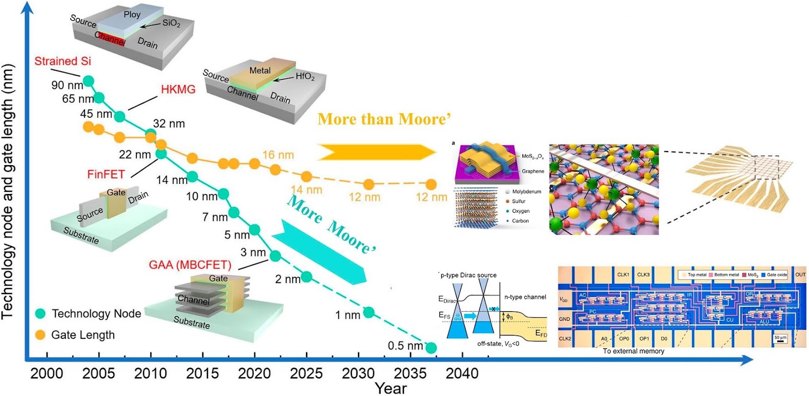
The relentless down-scaling of electronics grands the modern integrated circuits (ICs) with the high speed, low power dissipation and low cost, fulfilling diverse demands of modern life. Whereas, with the semiconductor industry entering into sub-10 nm technology nodes, degrading device performance and increasing power consumption give rise to insurmountable roadblocks confronted by modern ICs that need to be conquered to sustain the Moore law's life. Bulk semiconductors like prevalent Si are plagued by seriously degraded carrier mobility as thickness thinning down to sub-5 nm, which is imperative to maintain sufficient gate electrostatic controllability to combat the increasingly degraded short channel effects. Nowadays, the emergence of two-dimensional (2D) materials opens up new gateway to eschew the hurdles laid in front of the scaling trend of modern IC, mainly ascribed to their ultimately atomic thickness, capability to maintain carrier mobility with thickness thinning down, dangling-bonds free surface, wide bandgaps tunability and feasibility to constitute diverse heterostructures. Blossoming breakthroughs in discrete electronic device, such as contact engineering, dielectric integration and vigorous channel-length scaling, or large circuits arrays, as boosted yields, improved variations and full-functioned processor fabrication, based on 2D materials have been achieved nowadays, facilitating 2D materials to step under the spotlight of IC industry to be treated as the most potential future successor or complementary counterpart of incumbent Si to further sustain the down-scaling of modern IC.
1. Introduction
Since Gordon Moore proposed his famous Moore's law in 1965 [1], integrated circuits doubled every two years, manifesting by physical dimensions of discrete electronic device reducing by 0.7 times, ascribed to which the footprint reduces by ~0.5 times. On the contrary, operating speed doubles, power dissipation and cost both decrement by a factor of two [2, 3]. The Moore's law had been complied with integrated circuits (ICs) happily during the former several decades until semiconductor industry entered into sub-100 nm node, where gate began to give over part of its electrostatic dominance over channel to drain bias attributed to drain's stealing behavior over channel barrier [4, 5]. In this context, the notorious short channel effects (SCEs) began to come into view and draw themselves enormous attention to be dedicated efforts to [6].
The prominent SCEs that seriously degrade device performance comprise of subthreshold swing (SS), drain-induced barrier lower (DIBL), punch-through, Subthreshold-voltage (Vt) rolling off in accordance with channel length scaling and leakage current increasing [7–10]. SS describes the switching capability of the device and the smaller the SS, the stronger the gate electrostatic control over channel is, and DIBL is on behalf of the competing behavior of drain bias over the controllability of channel with regards to gate bias. Punch-through denotes the phenomenon of the depletion region induced by source and drain doping jointing with each other under the channel region, contributing to leakage current increment, while Vt rolling off contributes to leakage current escalating and stability issue in circuits, where leakage current increasing finally results in static power consumption surging.
The relentless downscaling of electronics poses imperative requests for novel device structures or ingenious materials which can reach a tradeoff between high discrete device performance and low power dissipation to sustain the Moore's law life further, this regime of semiconductor technology is termed as More Moore. For another, modern life brings forwards the requirements for 5G or 6G communication, cloud computing, artificial intelligent and neuromorphic computing, which all comes following the blossoming of More than Moore.
Loading authentic research manuscript (Pages 1–5)...
Laixiang Qin, Li Wang (2025). Two-Dimensional Materials, the Ultimate Solution for Future Electronics and Very-Large-Scale Integrated Circuits. Nano-Micro Letters. https://doi.org/10.1007/s40820-025-01769-2
Research & Educational Purpose Only:The translations, structured abstracts, analytical annotations, and data reports provided by SinoTechIntel are intended exclusively for academic research, internal corporate R&D, and educational benchmarking. They do not constitute formal engineering, chemical safety, legal, or professional advice.
Copyright & Intellectual Property Notice: Original copyright of the underlying source articles and experimental data remains with the respective authors, institutions, and original publishing journals. SinoTechIntel claims intellectual property only over its proprietary translations, analytical syntheses, and AEO structured enhancements in accordance with international fair use and academic citation principles.
Frequently Asked Questions
What are the main advantages of 2D materials for future electronics?
2D materials offer atomic thickness, maintain carrier mobility even at sub-5 nm, have dangling-bond-free surfaces, tunable bandgaps, and can form diverse heterostructures, making them ideal for overcoming the scaling limits of silicon.
How do 2D materials address short channel effects?
Their ultimate thinness enhances gate electrostatic control, reducing short channel effects like subthreshold swing degradation, drain-induced barrier lowering, and leakage currents, which are critical for continued scaling.
What challenges remain for large-scale integration of 2D materials?
Challenges include producing large-area, high-quality 2D materials with electronic-grade uniformity, developing mature fabrication techniques, and integrating them into existing CMOS processes.
What recent breakthroughs have been achieved in 2D material-based circuits?
Recent progress includes improved contact engineering, high-k dielectric integration, aggressive channel length scaling, and the demonstration of full-functioned processors, showing potential for future VLSI applications.
Are 2D materials expected to replace silicon?
2D materials are seen as potential successors or complementary to silicon, especially for future nodes where silicon faces fundamental limits, but they may initially be used in hybrid or specialized applications.
Related Technical Papers & Translations
Direct Repair of the Crystal Structure and Coating Surface of Spent LiFePO4 Materials Enables Superfast Li-Ion Migration
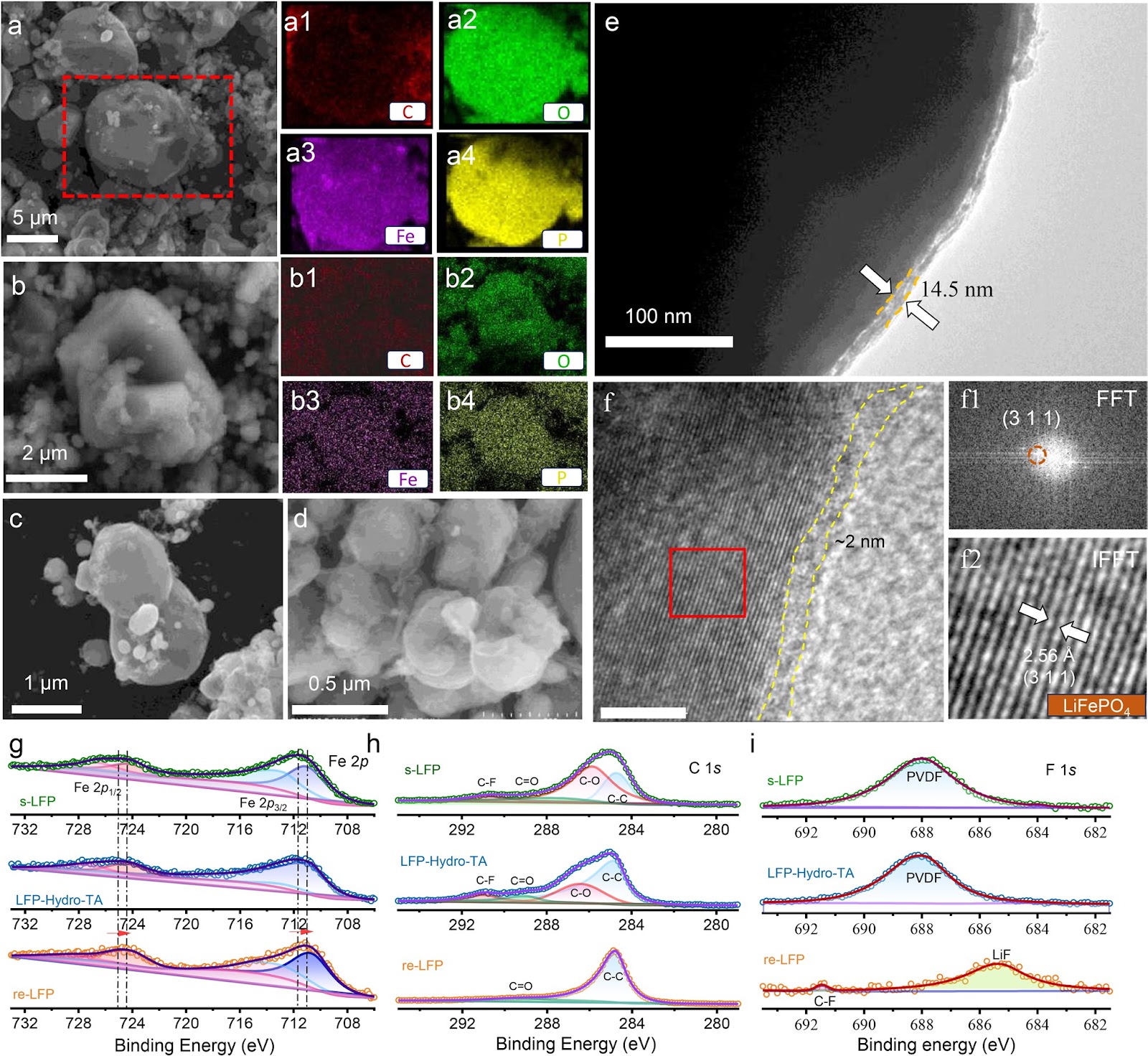
The rapid accumulation of spent LiFePO4 (LFP) cathodes from retired lithium-ion batteries necessitates the development of effective and environmental-friendly recycling strategies. In this context, direct regeneration has emerged as a promising approach for reclaiming LFP cathode materials, offering a streamlined pathway to restore their electrochemical functionality. We report an integrated regeneration protocol that simultaneously repairs the degraded crystal structure and reconstructs the damaged carbon coating in spent LFP. The regenerated cathode material had superfast lithium-ion diffusion kinetics and a stable cathode–electrolyte interface, giving a remarkable rate capability with specific capacities of 122 mAh g−1 at 5C and 106 mAh g−1 at 10C (1C = 170 mA g−1). It also maintained capacities of 110.7 mAh g−1 (5C) and 84.1 mAh g−1 (10C) after 400 cycles. It could be used in harsh environments and could be stably cycled at subzero temperatures (−10 and −20 °C) and in solid-state electrolyte batteries. Life cycle assessment combined with economic evaluation using the EverBatt model reveals that this direct regeneration approach has high economic and environmental benefits.
Oxide Semiconductor for Advanced Memory Architectures: Atomic Layer Deposition, Key Requirement and Challenges
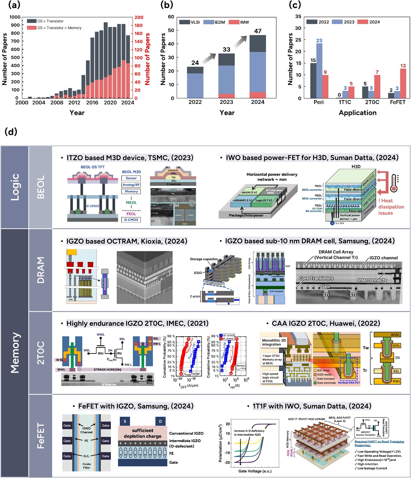
Oxide semiconductors (OSs), introduced by the Hosono group in the early 2000s, have evolved from display backplane materials to promising candidates for advanced memory and logic devices. The exceptionally low leakage current of OSs and compatibility with three-dimensional (3D) architectures have recently sparked renewed interest in their use in semiconductor applications. This review begins by exploring the unique material properties of OSs, which fundamentally originate from their distinct electronic band structure. Subsequently, we focus on atomic layer deposition (ALD), a core technique for growing excellent OS films, covering both basic and advanced processes compatible with 3D scaling. The basic surface reaction mechanisms—adsorption and reaction—and their roles in film growth are introduced. Furthermore, material design strategies, such as cation selection, crystallinity control, anion doping, and heterostructure engineering, are discussed. We also highlight challenges in memory applications, including contact resistance, hydrogen instability, and lack of p-type materials, and discuss the feasibility of ALD-grown OSs as potential solutions. Lastly, we provide an outlook on the role of ALD-grown OSs in memory technologies. This review bridges material fundamentals and device-level requirements, offering a comprehensive perspective on the potential of ALD-driven OSs for next-generation semiconductor memory devices.
Laser powder bed fusion of biodegradable Zn-4Cu alloy: Processing, microstructure and properties
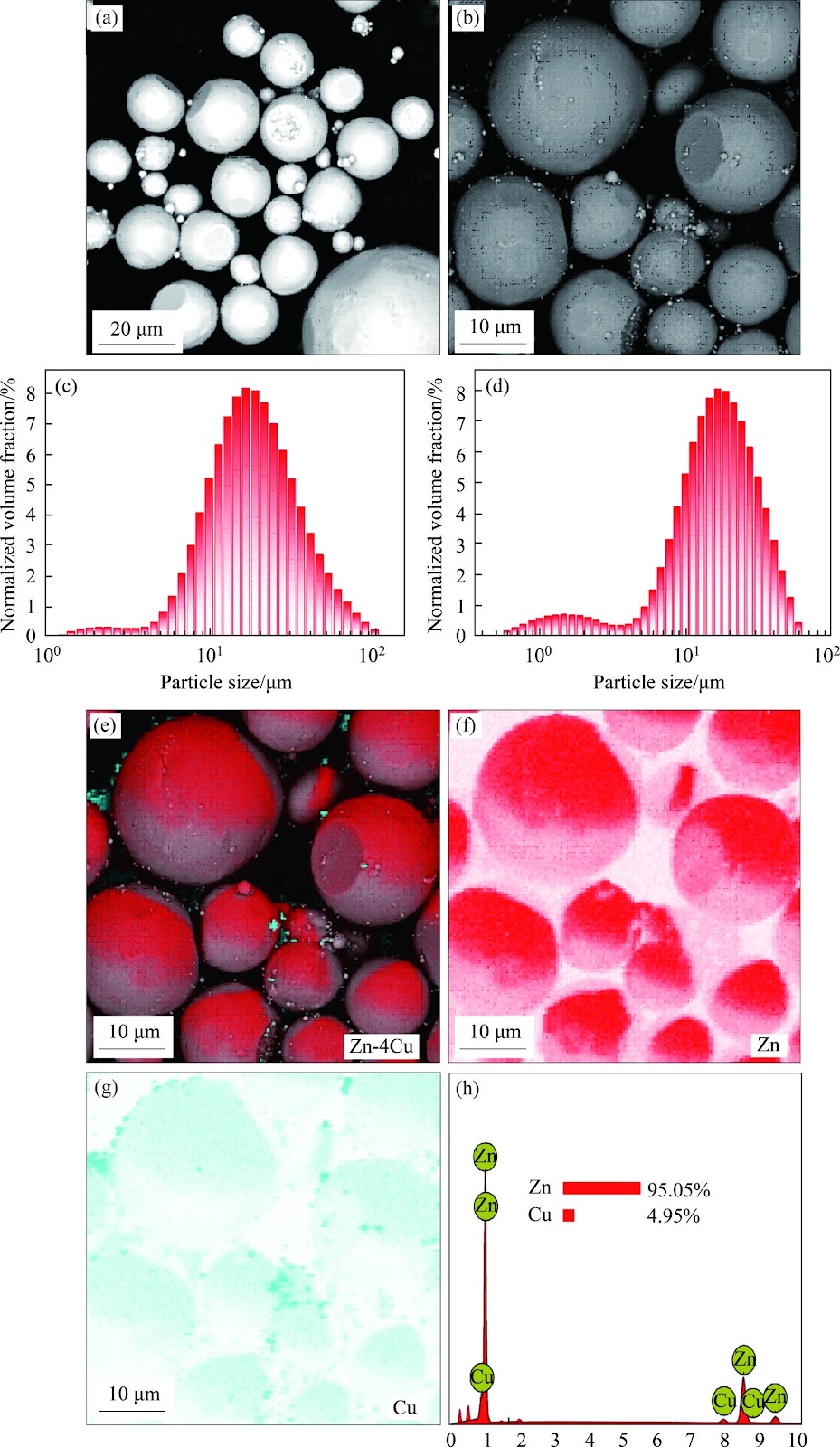
Zn's natural degradability and biocompatibility make it a promising candidate for implants, however, its mechanical properties remain insufficient for bone applications. In this study, the performance of Zn was enhanced by developing Zn-Cu alloys via laser powder bed fusion (LPBF). Optimal LPBF parameters for forming stable tracks were achieved by adjusting laser power and scanning speed. Under optimized conditions of 100 W and 100 mm/s, high-density (99.58%) Zn-Cu alloys with improved hardness (68.2HV) and yield strength (160 MPa) were achieved. These improvements are attributed to solid solution strengthening, segregation strengthening, and grain refinement. The Zn-Cu alloys also demonstrated favorable degradation behavior, with a rate of 0.16 mm/year. This degradation is primarily driven by micro-galvanic corrosion between the CuZn5 phase and Zn matrix, along with refined grains and increased grain boundary density. This work demonstrates a viable strategy for fabricating Zn-based implants with enhanced structural integrity and mechanical performance via LPBF.