Key Takeaways & Executive Findings
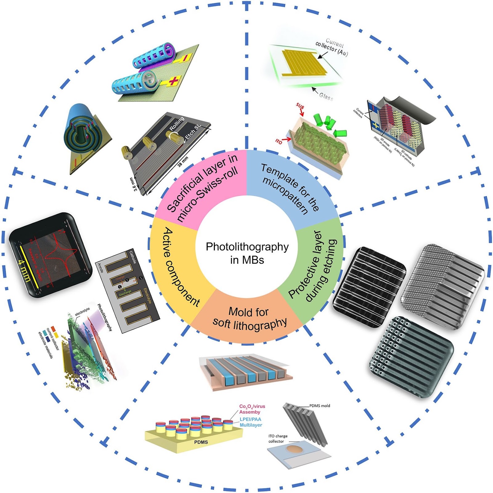
- •• Photolithography offers unparalleled resolution and design flexibility, making it ideal for fabricating microbatteries with precise micropatterns and complex 3D architectures. • The technique serves multiple roles in MB fabrication: as a template for 2D/3D micropatterns, a protective layer during etching, a mold for soft lithography, a component of active materials, and a sacrificial layer for micro-Swiss-roll structures. • Challenges remain in materials selection, packaging, and performance evaluation, but photolithographic MBs hold promise for powering IoT devices with on-chip energy storage. • This review provides a comprehensive framework for understanding photolithographic microfabrication, guiding future research and development in miniaturized energy storage.
Abstract
Microbatteries (MBs) are crucial to power miniaturized devices for the Internet of Things. In the evolutionary journey of MBs, fabrication technology emerges as the cornerstone, guiding the intricacies of their configuration designs, ensuring precision, and facilitating scalability for mass production. Photolithography stands out as an ideal technology, leveraging its unparalleled resolution, exceptional design flexibility, and entrenched position within the mature semiconductor industry. However, comprehensive reviews on its application in MB development remain scarce. This review aims to bridge that gap by thoroughly assessing the recent status and promising prospects of photolithographic microfabrication for MBs. Firstly, we delve into the fundamental principles and step-by-step procedures of photolithography, offering a nuanced understanding of its operational mechanisms and the criteria for photoresist selection. Subsequently, we highlighted the specific roles of photolithography in the fabrication of MBs, including its utilization as a template for creating miniaturized micropatterns, a protective layer during the etching process, a mold for soft lithography, a constituent of MB active component, and a sacrificial layer in the construction of micro-Swiss-roll structure. Finally, the review concludes with a summary of the key challenges and future perspectives of MBs fabricated by photolithography, providing comprehensive insights and sparking research inspiration in this field.
1. Introduction
With the continuous development of microelectronics and microsystems, the Internet of Things (IoT) era characterized by digitalization, intelligence, and the “interconnection of all things” is coming [1–6]. Miniaturized electronic devices (MEDs) are significant parts of IoT, including micro-electro-mechanical systems, microsensors, intelligent electronic equipment, micro-robots, and implantable medical devices [7]. Complex tasks containing signal detection, information processing, mechanical actuation, and wireless communications can be accomplished by such MEDs, and the MEDs can be distributed everywhere to connect everything by their ultra-small size. Places inaccessible to traditional electronic devices, such as narrow areas inside machines, leaves or roots of crops, or even blood vessels inside the human body, can be arranged with MEDs [8]. By sensing various surrounding signals, intelligently analyzing and processing, and sending the data to the database by wireless transmission, MEDs can conveniently monitor the environment, agriculture, and medical health. Such an invisible net could connect everything, achieving the IoT and facilitating more efficient decision-making [5, 9].
Critically, the power supply serves as the cornerstone, enabling the functionality of all these MEDs and ensuring their seamless operation [10]. Although various kinds of energy from the environment can be harvested by solar cells, thermo-electric devices, and nanogenerators, these forms of energy are inherently unstable and discontinuous, hindering the steady operation of the MEDs [10]. Consequently, electrochemical energy storage devices such as batteries, with high energy density achieving continuous energy supply, are indispensable [9, 11–14]. Given that the size of MED is usually at the millimeter or even micron level, the batteries employed in these applications, also known as microbatteries (MBs), must possess ultra-small dimensions, customizable shapes, facile integration, and high energy density to meet the requirements of MEDs [6, 11, 14]. Regrettably, miniaturizing traditional batteries into MBs introduces challenges and more stringent criteria regarding configuration design, microfabrication technology, and material selection [10]. The configuration of traditional batteries, such as coin-type, cylinder-type, pouch-type, and prismatic-type, involves stacking or winding the cathode, anode, and separator together [15–17]. However, due to the tiny size and high precision requirements, the st
Loading authentic research manuscript (Pages 1–5)...
Yuan Ma, Sen Wang, Zhong-Shuai Wu (2025). Photolithographic Microfabrication of Microbatteries for On-Chip Energy Storage. Nano-Micro Letters. https://doi.org/10.1007/s40820-024-01625-9
Research & Educational Purpose Only:The translations, structured abstracts, analytical annotations, and data reports provided by SinoTechIntel are intended exclusively for academic research, internal corporate R&D, and educational benchmarking. They do not constitute formal engineering, chemical safety, legal, or professional advice.
Copyright & Intellectual Property Notice: Original copyright of the underlying source articles and experimental data remains with the respective authors, institutions, and original publishing journals. SinoTechIntel claims intellectual property only over its proprietary translations, analytical syntheses, and AEO structured enhancements in accordance with international fair use and academic citation principles.
Frequently Asked Questions
What is the role of photolithography in microbattery fabrication?
Photolithography is used as a template for creating 2D and 3D micropatterns, a protective layer during etching, a mold for soft lithography, a component of the active material, and a sacrificial layer for constructing micro-Swiss-roll structures.
Why are microbatteries important for the Internet of Things (IoT)?
Microbatteries provide a compact and reliable power source for miniaturized electronic devices, which are essential components of IoT systems, enabling continuous operation and wireless communication.
What are the key challenges in photolithographic microfabrication of microbatteries?
Challenges include selecting appropriate materials, developing effective packaging techniques, ensuring performance evaluation, and scaling up the fabrication process for mass production.
What are the future directions for microbatteries fabricated using photolithography?
Future directions involve improving energy density, enhancing cycle stability, integrating with on-chip electronics, and exploring new materials and architectures to meet the demands of advanced IoT applications.
Related Technical Papers & Translations
Direct Repair of the Crystal Structure and Coating Surface of Spent LiFePO4 Materials Enables Superfast Li-Ion Migration
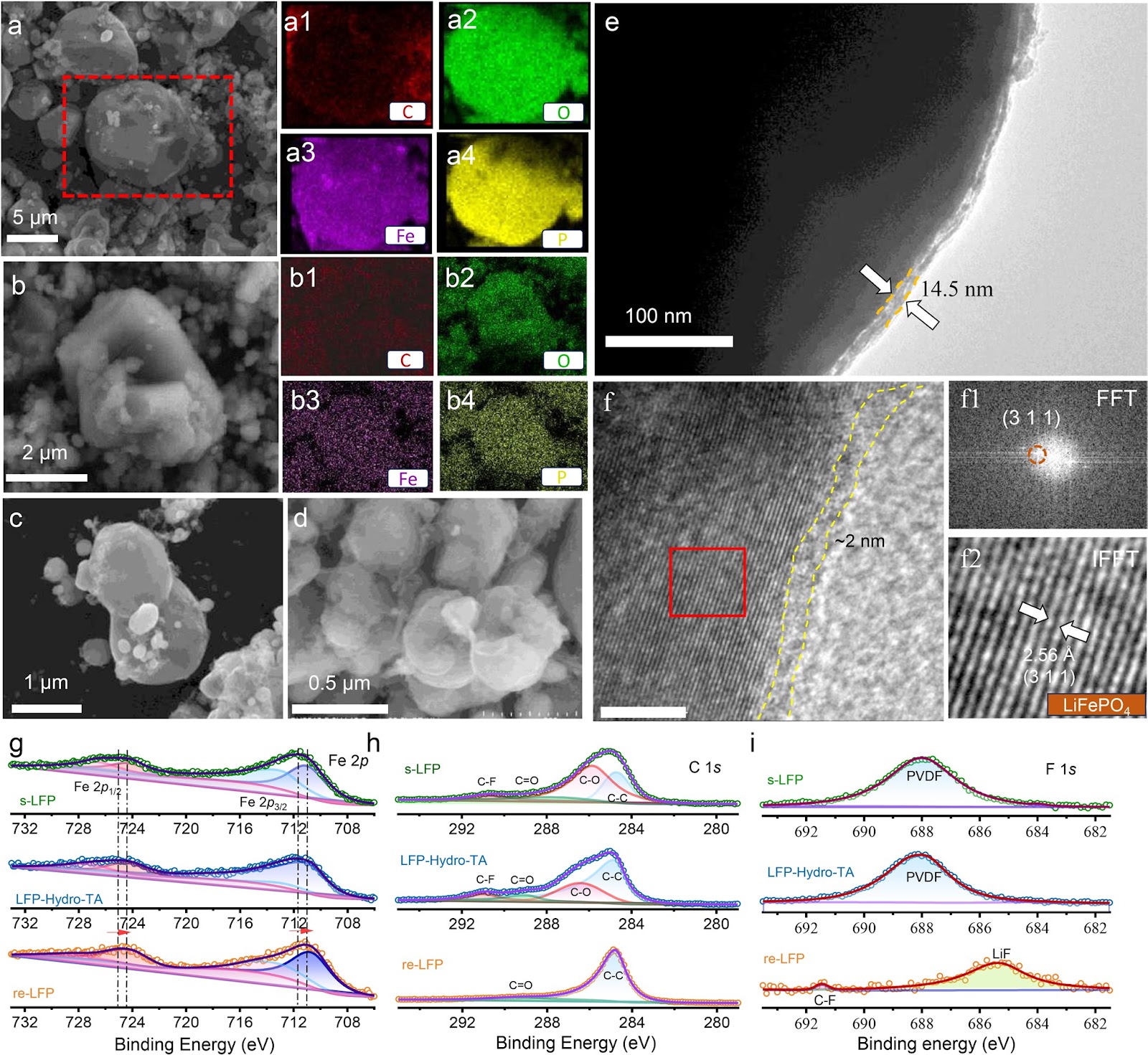
The rapid accumulation of spent LiFePO4 (LFP) cathodes from retired lithium-ion batteries necessitates the development of effective and environmental-friendly recycling strategies. In this context, direct regeneration has emerged as a promising approach for reclaiming LFP cathode materials, offering a streamlined pathway to restore their electrochemical functionality. We report an integrated regeneration protocol that simultaneously repairs the degraded crystal structure and reconstructs the damaged carbon coating in spent LFP. The regenerated cathode material had superfast lithium-ion diffusion kinetics and a stable cathode–electrolyte interface, giving a remarkable rate capability with specific capacities of 122 mAh g−1 at 5C and 106 mAh g−1 at 10C (1C = 170 mA g−1). It also maintained capacities of 110.7 mAh g−1 (5C) and 84.1 mAh g−1 (10C) after 400 cycles. It could be used in harsh environments and could be stably cycled at subzero temperatures (−10 and −20 °C) and in solid-state electrolyte batteries. Life cycle assessment combined with economic evaluation using the EverBatt model reveals that this direct regeneration approach has high economic and environmental benefits.
Oxide Semiconductor for Advanced Memory Architectures: Atomic Layer Deposition, Key Requirement and Challenges
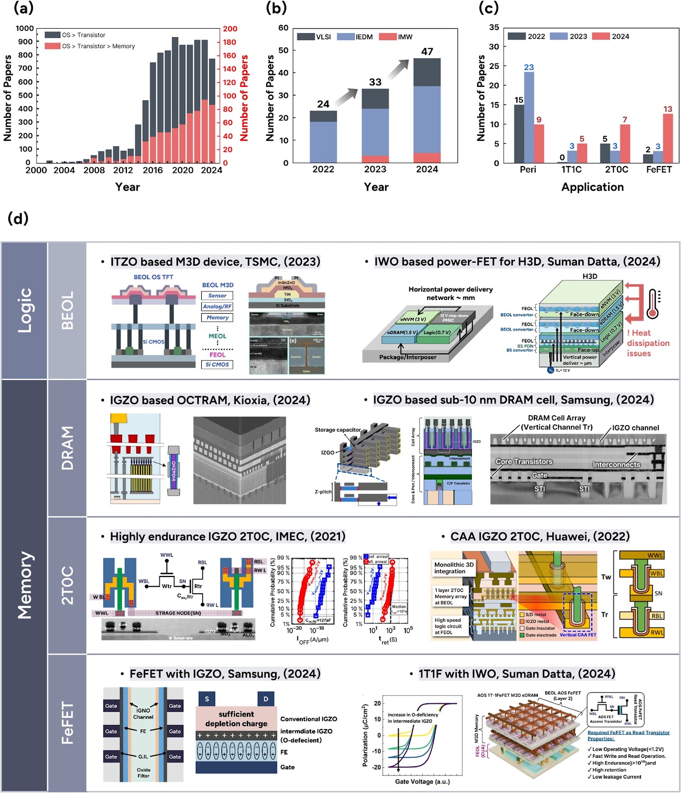
Oxide semiconductors (OSs), introduced by the Hosono group in the early 2000s, have evolved from display backplane materials to promising candidates for advanced memory and logic devices. The exceptionally low leakage current of OSs and compatibility with three-dimensional (3D) architectures have recently sparked renewed interest in their use in semiconductor applications. This review begins by exploring the unique material properties of OSs, which fundamentally originate from their distinct electronic band structure. Subsequently, we focus on atomic layer deposition (ALD), a core technique for growing excellent OS films, covering both basic and advanced processes compatible with 3D scaling. The basic surface reaction mechanisms—adsorption and reaction—and their roles in film growth are introduced. Furthermore, material design strategies, such as cation selection, crystallinity control, anion doping, and heterostructure engineering, are discussed. We also highlight challenges in memory applications, including contact resistance, hydrogen instability, and lack of p-type materials, and discuss the feasibility of ALD-grown OSs as potential solutions. Lastly, we provide an outlook on the role of ALD-grown OSs in memory technologies. This review bridges material fundamentals and device-level requirements, offering a comprehensive perspective on the potential of ALD-driven OSs for next-generation semiconductor memory devices.
Laser powder bed fusion of biodegradable Zn-4Cu alloy: Processing, microstructure and properties
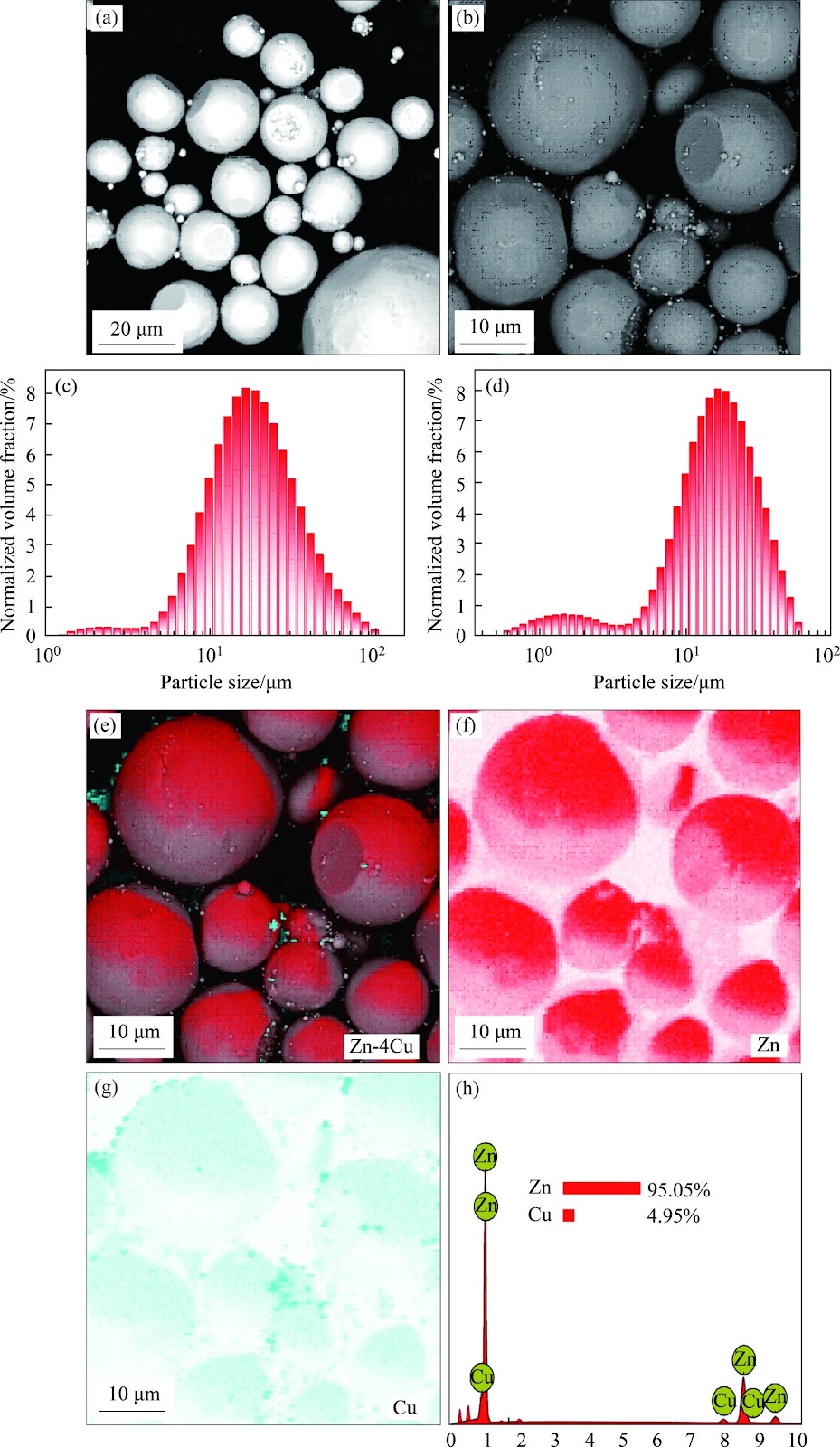
Zn's natural degradability and biocompatibility make it a promising candidate for implants, however, its mechanical properties remain insufficient for bone applications. In this study, the performance of Zn was enhanced by developing Zn-Cu alloys via laser powder bed fusion (LPBF). Optimal LPBF parameters for forming stable tracks were achieved by adjusting laser power and scanning speed. Under optimized conditions of 100 W and 100 mm/s, high-density (99.58%) Zn-Cu alloys with improved hardness (68.2HV) and yield strength (160 MPa) were achieved. These improvements are attributed to solid solution strengthening, segregation strengthening, and grain refinement. The Zn-Cu alloys also demonstrated favorable degradation behavior, with a rate of 0.16 mm/year. This degradation is primarily driven by micro-galvanic corrosion between the CuZn5 phase and Zn matrix, along with refined grains and increased grain boundary density. This work demonstrates a viable strategy for fabricating Zn-based implants with enhanced structural integrity and mechanical performance via LPBF.