Key Takeaways & Executive Findings
- •• Developed a modified near-infrared annealing (NIRA) system that achieves rapid and homogeneous crystallization of perovskite films within 20 seconds, drastically reducing processing time compared to conventional hot plate annealing (HPA). • The incorporation of excess PbI2 promotes consistent nucleation, enabling high-quality crystallization with performance surpassing that of HPA-based films. • Fully blade-coated perovskite solar modules achieved remarkable efficiencies of 22.03% (6×6 cm2, active area 18 cm2) and 20.18% (10×10 cm2, active area 56 cm2). • This work demonstrates the first successful homogeneous and high-quality crystallization in large-area perovskite films via rapid NIRA, significantly reducing energy consumption and manufacturing cycle, paving the way for commercial-scale production.
Abstract
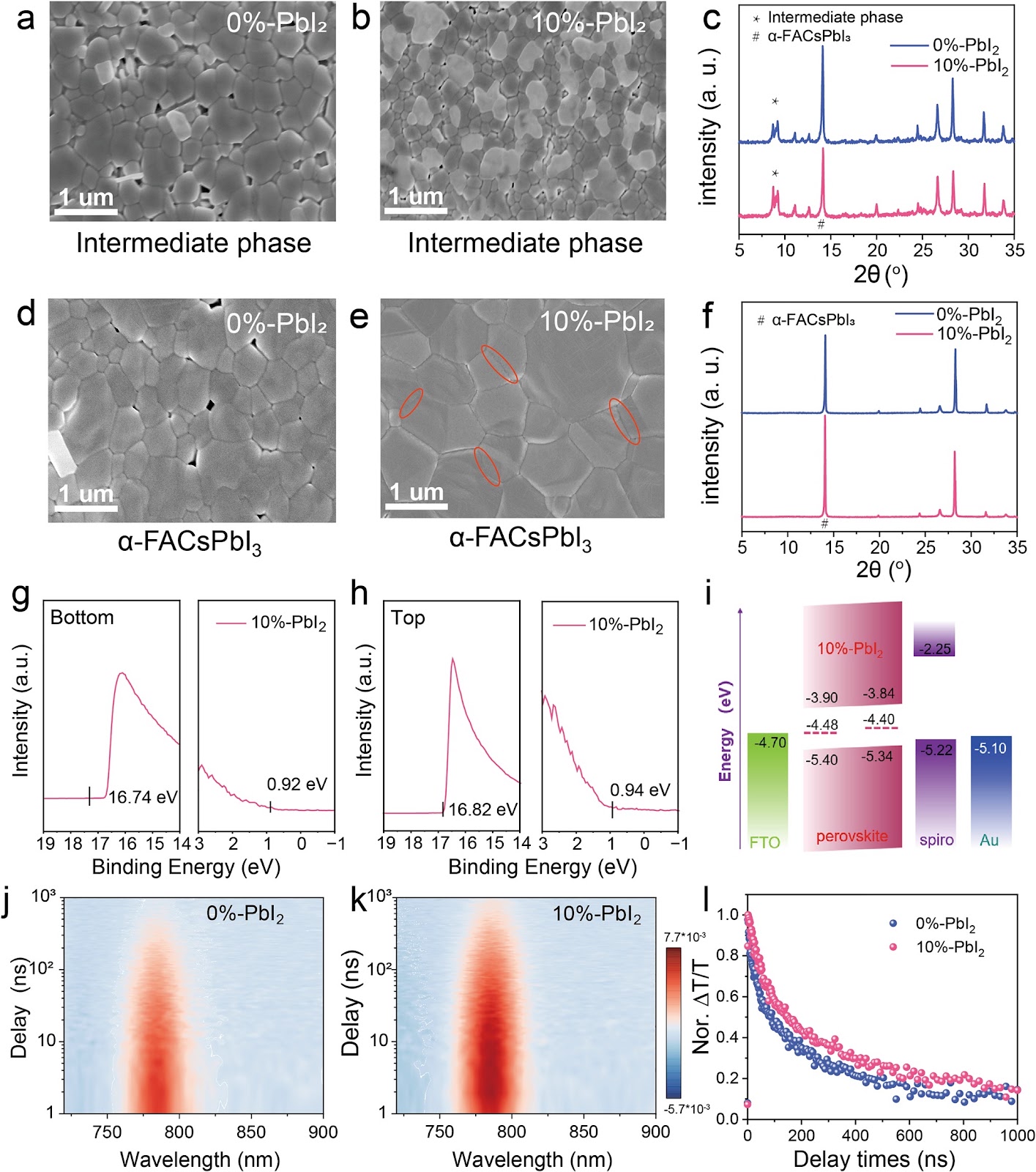
Currently, perovskite solar cells have achieved commendable progresses in power conversion efficiency (PCE) and operational stability. However, some conventional laboratory-scale fabrication methods become challenging when scaling up material syntheses or device production. Particularly, the prolonged high-temperature annealing process for the crystallization of perovskites requires a substantial amount of energy consumption and impact the modules’ throughput. Here, we report a modified near-infrared annealing (NIRA) process, which involves the excess PbI2 engineered crystallization, efficiently reduces the preparation time for perovskite active layer to within 20 s compared to dozens of min in conventional hot plate annealing (HPA) process. The study showed that the incorporated PbI2 promoted the consistent nucleation of the perovskite film, leading to the subsequent rapid and homogeneous crystallization at the NIRA stage. Thus, highly crystalized perovskite film was realized with even better crystallization performance than conventional HPA-based film. Ultimately, efficient perovskite solar modules of 36 and 100 cm2 were readily fabricated with the optimal PCEs of 22.03% and 20.18%, respectively. This study demonstrates, for the first time, the successful achievement of homogeneous and high-quality crystallization in large-area perovskite films through rapid NIRA processing. This approach not only significantly reduces energy consumption during production, but also substantially shortens the manufacturing cycle, paving a new path toward the commercial-scale application of perovskite solar modules.
1. Introduction
The lead halide perovskites have emerged as promising candidates for efficient and cost-effective photovoltaic material [1–3]. Currently, the commercialization of perovskite solar cells (PSCs) has gained significant momentum in the renewable energy sector [4, 5]. However, for large-area perovskite film fabrication, following the rapid solvent removal achieved through vacuum-flash evaporation or air-knife assisted techniques, thermal annealing must be precisely controlled for the final high-quality and uniform crystallization. The conventional thermal annealing process has drawn significant concern due to its time-consuming nature, expensive equipment requirements, and high energy consumption, which is the key bottleneck for large-scale preparation and throughput. Almost all high-performance PSCs with power conversion efficiencies exceeding 22% heavily rely on the conventional heat conduction method at temperatures > 100 °C for over 10 min. While, when scaling up the perovskite solar modules (PSMs) toward the industrialization, this process generally based on hot-plates become more and more difficult to implement for the controllable homogeneous crystallization besides energy and time consumptions [6, 7].
Reports have presented alternative techniques, such as microwave radiation annealing (MAP), intense pulse annealing (IAP) or near-infrared radiation annealing (NIRA), to facilitate the rapid preparation of perovskite thin films within seconds to minutes [8–10]. Among them, the NIRA annealing, typically utilizing near-infrared light with wavelengths ranging from 780 to 1400 nm, exhibits promising in enhancing the efficiency of energy transfer due to its simultaneous utilization of multiple heat transfer pathways including heat conduction, radiation and convection. This technology was pioneered by Watson et al. in 2015 to prepare a perovskite solar cell in an area of 0.1 cm2 with the efficiency of 10.7% by reducing the film annealing time to 2.5 s [11]. Subsequently, in 2019, Sandy Sanchez et al. further reduced the preparation time of perovskite films to 1.2 s through infrared fast heat treatment process combined with spin coating technology, and successfully prepared a perovskite single cell (aperture area of ...
Loading authentic research manuscript (Pages 1–5)...
Qing Chang, Peng He, Haosong Huang, Yingchen Peng, Xiao Han, Yang Shen, Jun Yin, Zhengjing Zhao, Ye Yang, Binghui Wu, Zhiguo Zhao, Jing Li, Nanfeng Zheng (2025). Modified Near-Infrared Annealing Enabled Rapid and Homogeneous Crystallization of Perovskite Films for Efficient Solar Modules. Nano-Micro Letters. https://doi.org/10.1007/s40820-025-01792-3
Research & Educational Purpose Only:The translations, structured abstracts, analytical annotations, and data reports provided by SinoTechIntel are intended exclusively for academic research, internal corporate R&D, and educational benchmarking. They do not constitute formal engineering, chemical safety, legal, or professional advice.
Copyright & Intellectual Property Notice: Original copyright of the underlying source articles and experimental data remains with the respective authors, institutions, and original publishing journals. SinoTechIntel claims intellectual property only over its proprietary translations, analytical syntheses, and AEO structured enhancements in accordance with international fair use and academic citation principles.
Frequently Asked Questions
What is the main innovation of this paper?
The paper introduces a modified near-infrared annealing (NIRA) process that enables rapid and homogeneous crystallization of perovskite films within 20 seconds, significantly reducing processing time and energy consumption compared to conventional hot plate annealing.
How does the NIRA process achieve rapid crystallization?
The NIRA process utilizes near-infrared light (780-1400 nm) which provides multiple heat transfer pathways (conduction, radiation, convection) for efficient energy transfer. The incorporation of excess PbI2 promotes consistent nucleation, leading to rapid and homogeneous crystallization.
What efficiencies were achieved for perovskite solar modules?
The fully blade-coated perovskite solar modules achieved efficiencies of 22.03% for a 6×6 cm2 module (active area 18 cm2) and 20.18% for a 10×10 cm2 module (active area 56 cm2).
What are the advantages of NIRA over conventional annealing?
NIRA reduces the annealing time from dozens of minutes to under 20 seconds, lowers energy consumption, and enables homogeneous crystallization over large areas, which is crucial for commercial-scale production.
What is the significance of this work for perovskite solar cell commercialization?
This work demonstrates a scalable, rapid annealing method that maintains high efficiency and quality, addressing key bottlenecks in throughput and energy use, thus paving the way for industrial production of perovskite solar modules.
Related Technical Papers & Translations
Direct Repair of the Crystal Structure and Coating Surface of Spent LiFePO4 Materials Enables Superfast Li-Ion Migration
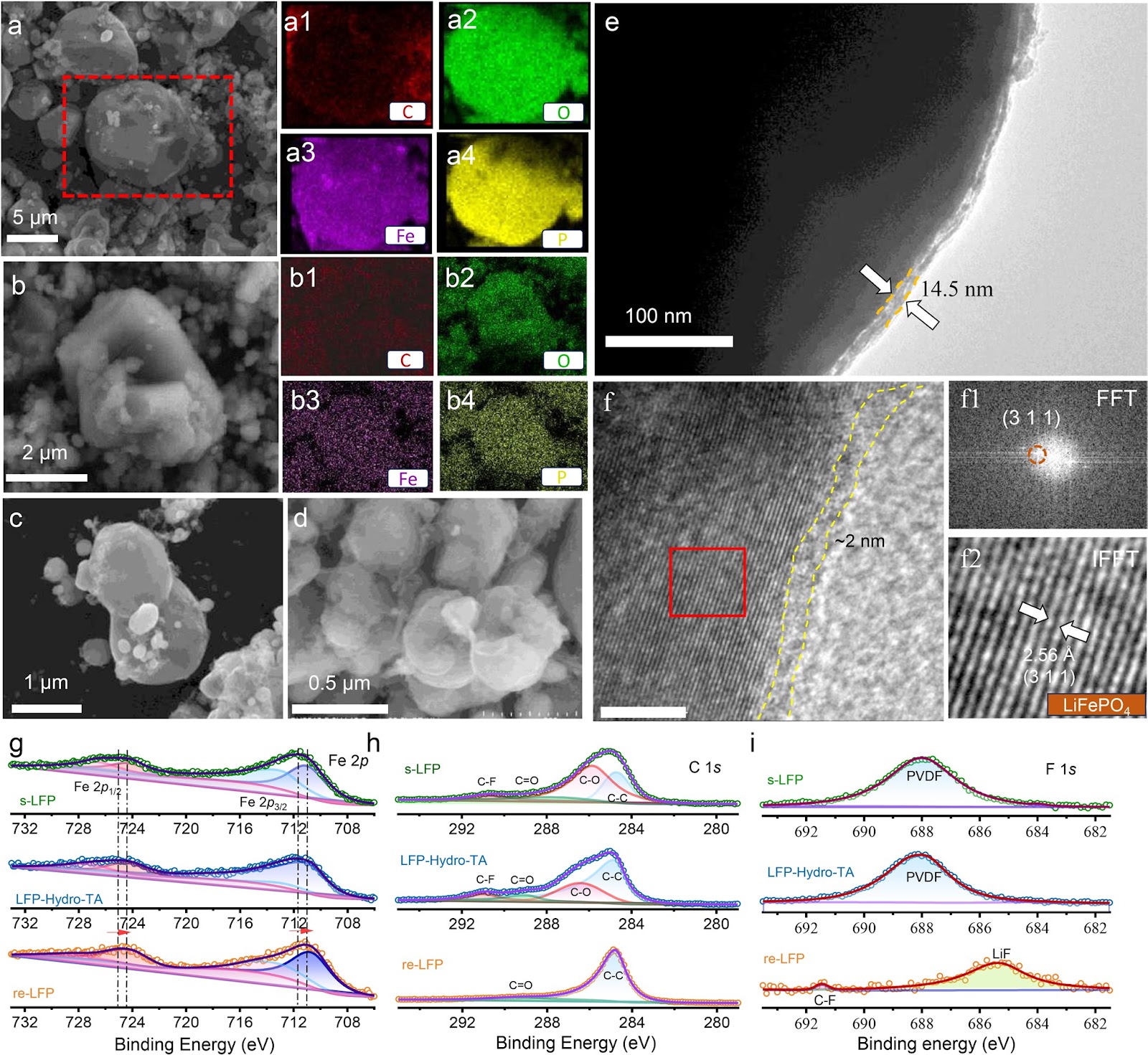
The rapid accumulation of spent LiFePO4 (LFP) cathodes from retired lithium-ion batteries necessitates the development of effective and environmental-friendly recycling strategies. In this context, direct regeneration has emerged as a promising approach for reclaiming LFP cathode materials, offering a streamlined pathway to restore their electrochemical functionality. We report an integrated regeneration protocol that simultaneously repairs the degraded crystal structure and reconstructs the damaged carbon coating in spent LFP. The regenerated cathode material had superfast lithium-ion diffusion kinetics and a stable cathode–electrolyte interface, giving a remarkable rate capability with specific capacities of 122 mAh g−1 at 5C and 106 mAh g−1 at 10C (1C = 170 mA g−1). It also maintained capacities of 110.7 mAh g−1 (5C) and 84.1 mAh g−1 (10C) after 400 cycles. It could be used in harsh environments and could be stably cycled at subzero temperatures (−10 and −20 °C) and in solid-state electrolyte batteries. Life cycle assessment combined with economic evaluation using the EverBatt model reveals that this direct regeneration approach has high economic and environmental benefits.
Oxide Semiconductor for Advanced Memory Architectures: Atomic Layer Deposition, Key Requirement and Challenges
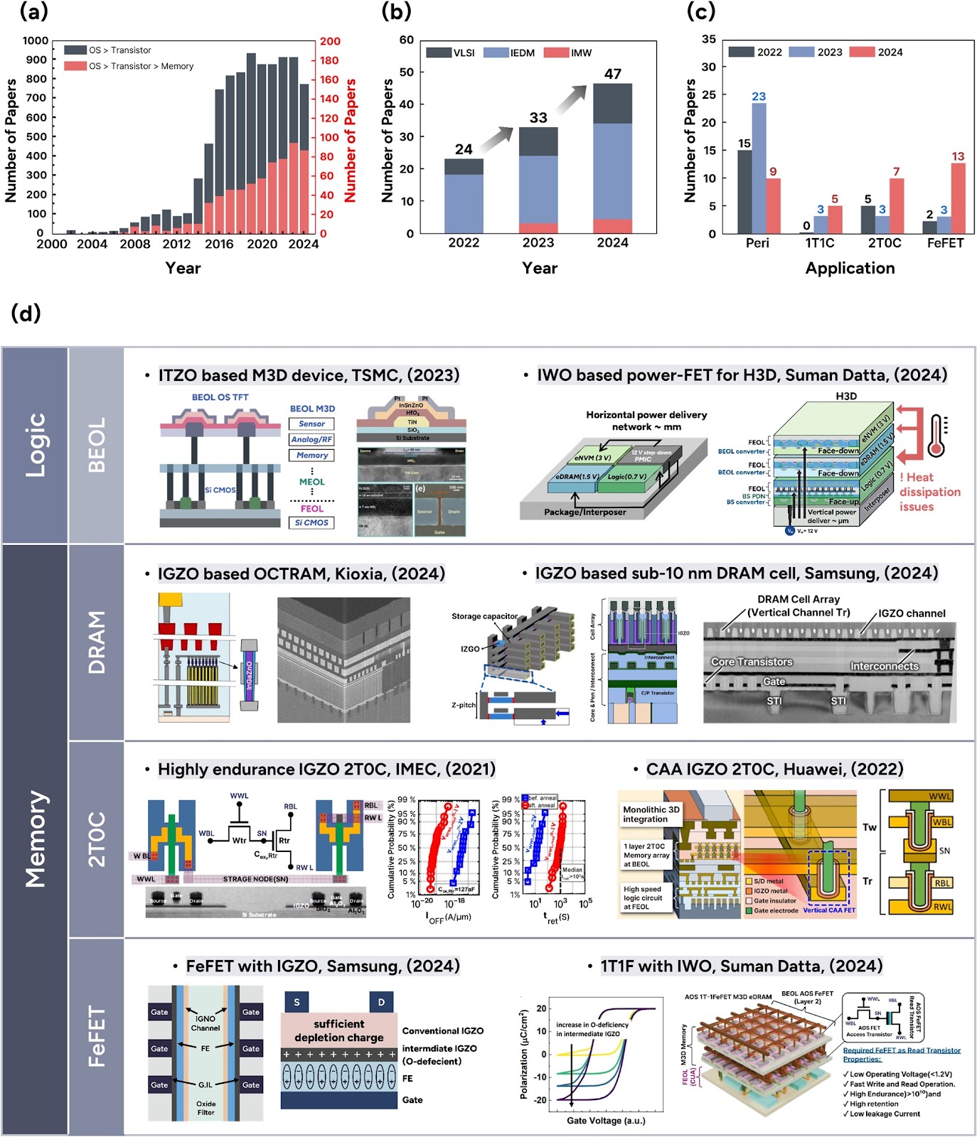
Oxide semiconductors (OSs), introduced by the Hosono group in the early 2000s, have evolved from display backplane materials to promising candidates for advanced memory and logic devices. The exceptionally low leakage current of OSs and compatibility with three-dimensional (3D) architectures have recently sparked renewed interest in their use in semiconductor applications. This review begins by exploring the unique material properties of OSs, which fundamentally originate from their distinct electronic band structure. Subsequently, we focus on atomic layer deposition (ALD), a core technique for growing excellent OS films, covering both basic and advanced processes compatible with 3D scaling. The basic surface reaction mechanisms—adsorption and reaction—and their roles in film growth are introduced. Furthermore, material design strategies, such as cation selection, crystallinity control, anion doping, and heterostructure engineering, are discussed. We also highlight challenges in memory applications, including contact resistance, hydrogen instability, and lack of p-type materials, and discuss the feasibility of ALD-grown OSs as potential solutions. Lastly, we provide an outlook on the role of ALD-grown OSs in memory technologies. This review bridges material fundamentals and device-level requirements, offering a comprehensive perspective on the potential of ALD-driven OSs for next-generation semiconductor memory devices.
Laser powder bed fusion of biodegradable Zn-4Cu alloy: Processing, microstructure and properties
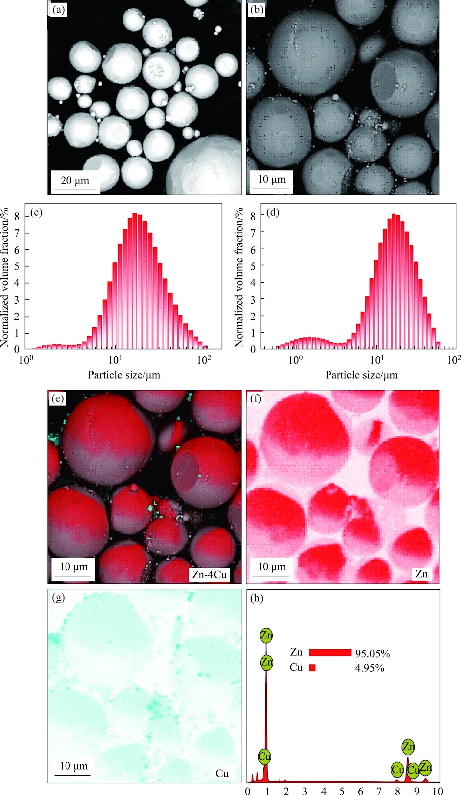
Zn's natural degradability and biocompatibility make it a promising candidate for implants, however, its mechanical properties remain insufficient for bone applications. In this study, the performance of Zn was enhanced by developing Zn-Cu alloys via laser powder bed fusion (LPBF). Optimal LPBF parameters for forming stable tracks were achieved by adjusting laser power and scanning speed. Under optimized conditions of 100 W and 100 mm/s, high-density (99.58%) Zn-Cu alloys with improved hardness (68.2HV) and yield strength (160 MPa) were achieved. These improvements are attributed to solid solution strengthening, segregation strengthening, and grain refinement. The Zn-Cu alloys also demonstrated favorable degradation behavior, with a rate of 0.16 mm/year. This degradation is primarily driven by micro-galvanic corrosion between the CuZn5 phase and Zn matrix, along with refined grains and increased grain boundary density. This work demonstrates a viable strategy for fabricating Zn-based implants with enhanced structural integrity and mechanical performance via LPBF.