Key Takeaways & Executive Findings
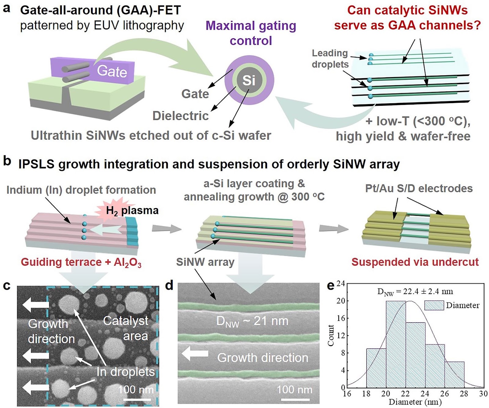
- •• A high-density array of orderly silicon nanowires (SiNWs) was grown in precise locations, with diameter of DNW = 22.4 ± 2.4 nm and interwire spacing of 90 nm. • A special suspension-contact protocol has been developed to reliably suspend the in-plane solid-liquid-solid SiNWs to serve as ultrathin quasi-1D channels for gate-all-around field-effect transistors (GAA-FETs). • By optimizing the source/drain metal contacts, high-performance catalytical GAA-FETs have been successfully demonstrated, achieving a high on/off current ratio of 10^7 and a steep subthreshold swing of 66 mV dec−1. • The results indicate that catalytic IPSLS SiNWs can serve as ideal 1D channels for scalable fabrication of high-performance GAA-FETs, well suited for monolithic 3D integrations.
Abstract
Gate-all-around field-effect transistors (GAA-FETs) represent the leading-edge channel architecture for constructing state-of-the-art high-performance FETs. Despite the advantages offered by the GAA configuration, its application to catalytic silicon nanowire (SiNW) channels, known for facile low-temperature fabrication and high yield, has faced challenges primarily due to issues with precise positioning and alignment. In exploring this promising avenue, we employed an in-plane solid–liquid-solid (IPSLS) growth technique to batch-fabricate orderly arrays of ultrathin SiNWs, with diameters of DNW = 22.4 ± 2.4 nm and interwire spacing of 90 nm. An in situ channel-releasing technique has been developed to well preserve the geometry integrity of suspended SiNW arrays. By optimizing the source/drain contacts, high-performance GAA-FET devices have been successfully fabricated, based on these catalytic SiNW channels for the first time, yielding a high on/off current ratio of 10^7 and a steep subthreshold swing of 66 mV dec−1, closing the performance gap between the catalytic SiNW-FETs and state-of-the-art GAA-FETs fabricated by using advanced top-down EBL and EUV lithography. These results indicate that catalytic IPSLS SiNWs can also serve as the ideal 1D channels for scalable fabrication of high-performance GAA-FETs, well suited for monolithic 3D integrations.
1. Introduction
Gate-all-around field-effect transistors (GAA-FETs, as depicted in Fig. 1a), which offer exceptional electrostatic control, are becoming the mainstream device architecture for technology nodes < N3 nm [1–4], where ultrathin crystalline silicon nanowires (c-SiNWs) are considered as ideal quasi-one-dimensional (1D) channel materials to mitigate the short-channel effect in highly integrated CMOS logics. However, to implement monolithic 3D integration that enables higher integration density, it is essential to fabricate ultrathin SiNW channels on the stacked layers, where a monocrystalline Si wafer substrate is absent. Instead of using a conventional top-down etching procedure in the bottom logic layer, these 1D SiNW channels should be grown in precise locations as orderly arrays directly on the insulating dielectric layer, via a low-temperature process to avoid thermal damage to the underlying logic layers [5–7].
To address this challenge, a low-temperature catalytic growth of such SiNW channels provides an ideal option, as it doesn’t rely on the preexistence of c-Si wafer [8, 9]. Although the famous vapor–liquid-solid (VLS) growth mechanism has been widely exploited to produce high-quality SiNW channels for the demonstration of high-performance FETs and sensors [10–13], the vertical orientation of the VLS-grown SiNWs makes them difficult to integrate into the planar device architecture [14, 15]. Particularly, the post-growth transfer and release of individual VLS-SiNWs onto pre-defined electrode trench, for the subsequent formation of GAA-FET, lacks deterministic position and orientation control, and is thus technically incompatible with the standard planar manufacturing procedure [11, 16, 17]. In order to address this challenge, an in-plane solid–liquid-solid (IPSLS) mechanism [18–20] has been developed in our previous works, where indium (In) catalyst droplets absorb amorphous silicon (a-Si) precursor thin film to produce c-SiNWs along pre-defined guiding step edges. Indeed, a rather high-density integration of the IPSLS SiNWs has been demonstrated, under the guidance of terrace mini-steps [21, 22] or the sidewall grooves [23, 24], achieving an impressive diameter and uniformity control, backed by a series of tailored catalyst formation technologies [24, 25]. However, the performance of planar or GAA-FETs fabricated with catalytic SiNW channels still lags significantly behind that of state-of-the-art fin- or GAA gate FETs [11, 16, 17, 26]. Specifically, the subthreshold swing (SS) of the catalytic SiNW-FETs, a key indicator of the strength of electrostatic control, typically ranges from 850 to 100 mV dec−1 [27–33], which is still far from the theoretical limit of 60 mV dec−1. For the IPSLS SiNWs, a genuine GAA-FET has not yet been demonstrated, and their potential to serve as 1D channels for high-performance FETs remains to be explored and verified through direct experimental evidence.
In this work, we focus on demonstrating high-performance GAA-FETs based on orderly arrays of catalytic SiNW channels grown by IPSLS, achieving a high on/off current ratio of 10^7 and a steep subthreshold swing of 66 mV dec−1, thereby closing the performance gap with state-of-the-art GAA-FETs fabricated by advanced lithography.
Loading authentic research manuscript (Pages 1–5)...
Wei Liao, Wentao Qian, Junyang An, Lei Liang, Zhiyan Hu, Junzhuan Wang, Linwei Yu (2025). High-Performance Gate-All-Around Field Effect Transistors Based on Orderly Arrays of Catalytic Si Nanowire Channels. Nano-Micro Letters. https://doi.org/10.1007/s40820-025-01674-8
Research & Educational Purpose Only:The translations, structured abstracts, analytical annotations, and data reports provided by SinoTechIntel are intended exclusively for academic research, internal corporate R&D, and educational benchmarking. They do not constitute formal engineering, chemical safety, legal, or professional advice.
Copyright & Intellectual Property Notice: Original copyright of the underlying source articles and experimental data remains with the respective authors, institutions, and original publishing journals. SinoTechIntel claims intellectual property only over its proprietary translations, analytical syntheses, and AEO structured enhancements in accordance with international fair use and academic citation principles.
Frequently Asked Questions
What is the main achievement of this paper?
The paper demonstrates high-performance gate-all-around field-effect transistors (GAA-FETs) based on orderly arrays of catalytic silicon nanowires (SiNWs) grown by in-plane solid-liquid-solid (IPSLS) technique, achieving a high on/off current ratio of 10^7 and a steep subthreshold swing of 66 mV/dec, closing the performance gap with state-of-the-art GAA-FETs.
What is the in-plane solid-liquid-solid (IPSLS) growth technique?
IPSLS is a low-temperature catalytic growth method where indium catalyst droplets absorb amorphous silicon precursor thin film to produce crystalline silicon nanowires along pre-defined guiding step edges, enabling precise positioning and alignment for planar device integration.
What are the key parameters of the silicon nanowires fabricated in this study?
The silicon nanowires have a diameter of 22.4 ± 2.4 nm and an interwire spacing of 90 nm, forming high-density orderly arrays.
How does this work contribute to monolithic 3D integration?
The catalytic IPSLS SiNWs can be grown directly on insulating dielectric layers at low temperatures, avoiding thermal damage to underlying logic layers, making them suitable for monolithic 3D integration.
What is the significance of achieving a subthreshold swing of 66 mV/dec?
A subthreshold swing of 66 mV/dec is close to the theoretical limit of 60 mV/dec, indicating excellent electrostatic control and high performance, comparable to state-of-the-art GAA-FETs fabricated by advanced lithography.
Related Technical Papers & Translations
Direct Repair of the Crystal Structure and Coating Surface of Spent LiFePO4 Materials Enables Superfast Li-Ion Migration
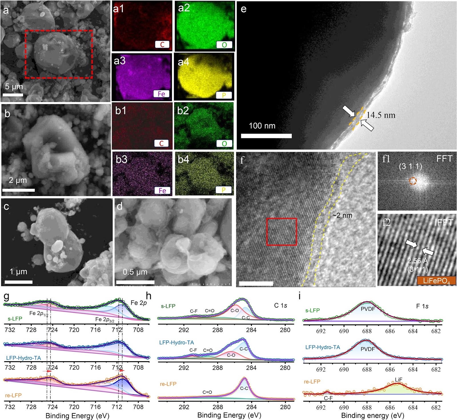
The rapid accumulation of spent LiFePO4 (LFP) cathodes from retired lithium-ion batteries necessitates the development of effective and environmental-friendly recycling strategies. In this context, direct regeneration has emerged as a promising approach for reclaiming LFP cathode materials, offering a streamlined pathway to restore their electrochemical functionality. We report an integrated regeneration protocol that simultaneously repairs the degraded crystal structure and reconstructs the damaged carbon coating in spent LFP. The regenerated cathode material had superfast lithium-ion diffusion kinetics and a stable cathode–electrolyte interface, giving a remarkable rate capability with specific capacities of 122 mAh g−1 at 5C and 106 mAh g−1 at 10C (1C = 170 mA g−1). It also maintained capacities of 110.7 mAh g−1 (5C) and 84.1 mAh g−1 (10C) after 400 cycles. It could be used in harsh environments and could be stably cycled at subzero temperatures (−10 and −20 °C) and in solid-state electrolyte batteries. Life cycle assessment combined with economic evaluation using the EverBatt model reveals that this direct regeneration approach has high economic and environmental benefits.
Oxide Semiconductor for Advanced Memory Architectures: Atomic Layer Deposition, Key Requirement and Challenges
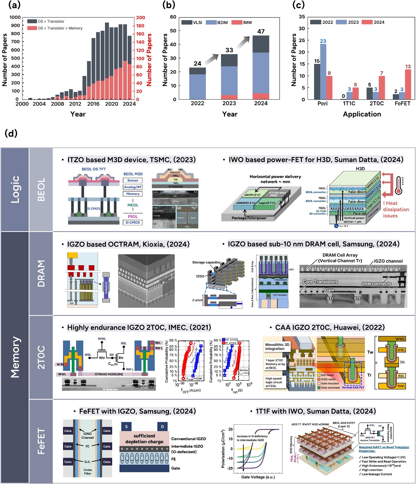
Oxide semiconductors (OSs), introduced by the Hosono group in the early 2000s, have evolved from display backplane materials to promising candidates for advanced memory and logic devices. The exceptionally low leakage current of OSs and compatibility with three-dimensional (3D) architectures have recently sparked renewed interest in their use in semiconductor applications. This review begins by exploring the unique material properties of OSs, which fundamentally originate from their distinct electronic band structure. Subsequently, we focus on atomic layer deposition (ALD), a core technique for growing excellent OS films, covering both basic and advanced processes compatible with 3D scaling. The basic surface reaction mechanisms—adsorption and reaction—and their roles in film growth are introduced. Furthermore, material design strategies, such as cation selection, crystallinity control, anion doping, and heterostructure engineering, are discussed. We also highlight challenges in memory applications, including contact resistance, hydrogen instability, and lack of p-type materials, and discuss the feasibility of ALD-grown OSs as potential solutions. Lastly, we provide an outlook on the role of ALD-grown OSs in memory technologies. This review bridges material fundamentals and device-level requirements, offering a comprehensive perspective on the potential of ALD-driven OSs for next-generation semiconductor memory devices.
Laser powder bed fusion of biodegradable Zn-4Cu alloy: Processing, microstructure and properties
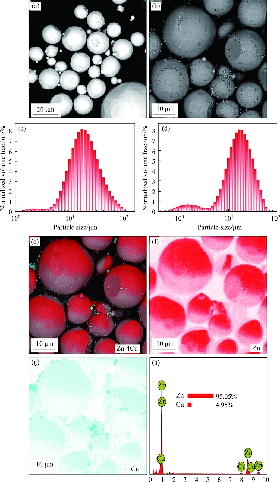
Zn's natural degradability and biocompatibility make it a promising candidate for implants, however, its mechanical properties remain insufficient for bone applications. In this study, the performance of Zn was enhanced by developing Zn-Cu alloys via laser powder bed fusion (LPBF). Optimal LPBF parameters for forming stable tracks were achieved by adjusting laser power and scanning speed. Under optimized conditions of 100 W and 100 mm/s, high-density (99.58%) Zn-Cu alloys with improved hardness (68.2HV) and yield strength (160 MPa) were achieved. These improvements are attributed to solid solution strengthening, segregation strengthening, and grain refinement. The Zn-Cu alloys also demonstrated favorable degradation behavior, with a rate of 0.16 mm/year. This degradation is primarily driven by micro-galvanic corrosion between the CuZn5 phase and Zn matrix, along with refined grains and increased grain boundary density. This work demonstrates a viable strategy for fabricating Zn-based implants with enhanced structural integrity and mechanical performance via LPBF.