SinoTechIntel Academic Portal
🏛️ Indexed Academic JournalImpact Factor: 3.8

Journal of Semiconductors (半导体学报 - 中国科学院半导体研究所)

Authoritative peer-reviewed journal in materials science, metallurgy, chemistry and engineering technologies: Journal of Semiconductors (半导体学报 - Viện Bán dẫn CAS)

Total Research Papers: 115
Access: 100% Free Open Access
Browse by Publication Year & VolumeReset All Filters ✕

Published Research PapersFiltered: Year 2025 • Vol. 32 • 12

Showing 5 of 115 peer-reviewed papers with full Graphical Abstracts.

Original ResearchVol. 32, Issue 12 • pp. 100-112DOI: 10.1088/1674-4926/25120029Jan 15, 2025

PL spectra and PL dynamics of CsPbBr3 quantum dots in solution and film

Authors: Zhengda Dong, Dachuan Li, Pingyuan Yan, Chuanxiang Sheng

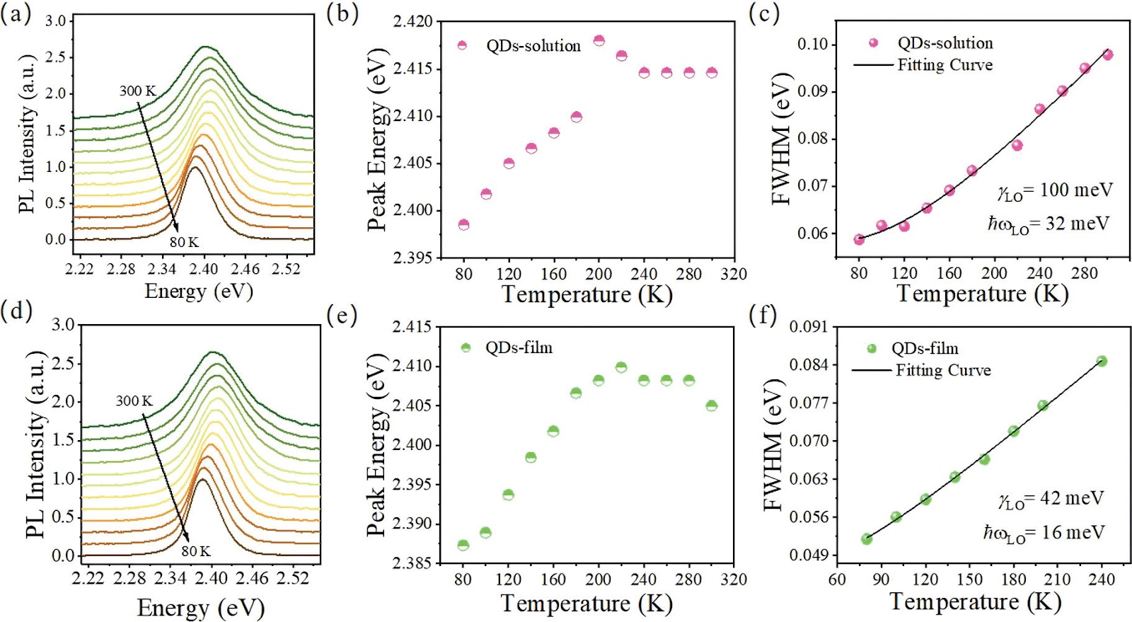
Temperature dependent photoluminescence (PL) and time-resolved PL (TRPL) of CsPbBr3 quantum dots (QDs) in solution and film are investigated. The electron−phonon coupling strength of quantum dots in solution is found two times larger than that of thin films. The averaged phonon energy involved in luminescence is also significantly higher than that of thin films, indicating that ligands’ phonons are involved in optical processes in solution but not in film. TRPL shows that the luminescence lifetime of the solution (22.5 ns) is longer than that of the thin film (5 ns) at room temperature, and both decrease abnormally with decreasing temperature, ascribing to the thermally activated trap states for PL, the further analysis shows that the trap energy levels in the thin film are deeper (~20 meV) compared to ~4 meV in solution. Our work proves that the morphology of organic ligands can regulate electron−phonon interactions and optoelectronic properties in CsPbBr3 QDs, providing fundamental insights into its photophysics.

PL spectra and PL dynamics of CsPbBr3 quantum dots in solution and film
Graphical Abstract
Original ResearchVol. 32, Issue 12 • pp. 100-112DOI: 10.1088/1674-4926/25120027Jan 15, 2025

A 2 mm × 2 mm Battery-Free Neural Interface Achieving 72-Channel Wireless Simultaneous Recording by Dual Overlapped On-Chip Antennas

Authors: Yili Shen, Yunshan Zhang, Changgui Yang, Yuxuan Luo, Bo Zhao

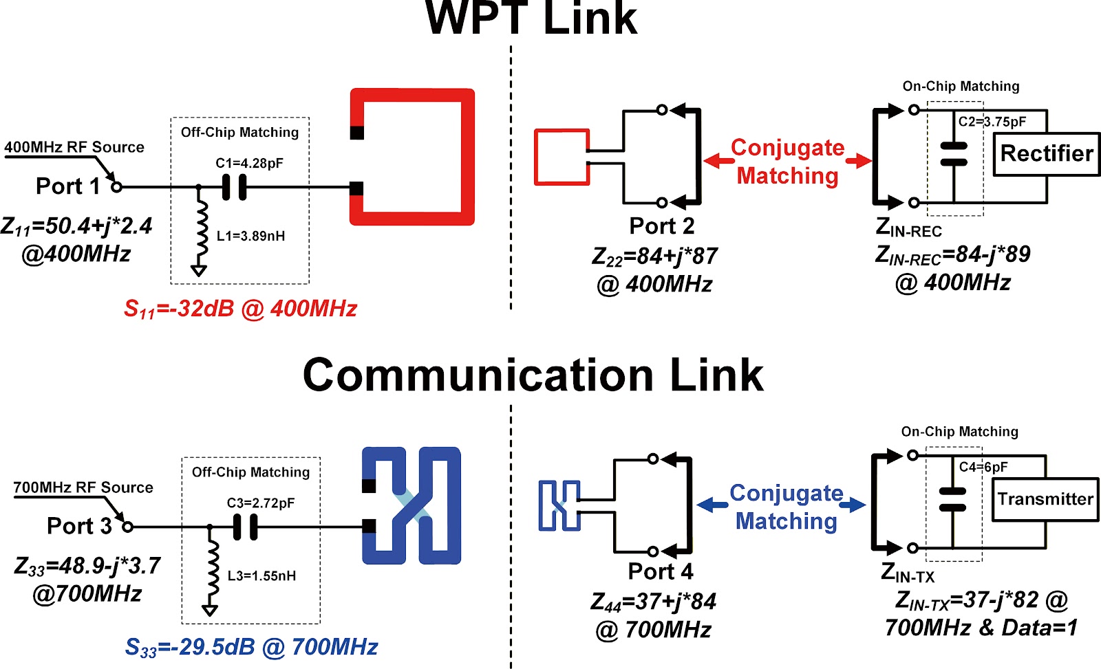
Battery-free radio systems utilizing wireless power transfer (WPT) further facilitate the miniaturization of neural implants. However, simultaneous monitoring of multiple neuronal activities is required to obtain high-fidelity neural signals. Consequently, the integration of numerous channels on a single chip and the wireless transmission of massive multi-channel data pose significant challenges for implantable battery-free neural interfaces. This work introduces dual overlapped on-chip antennas to eliminate the need for a battery in the neural implants and enable high-data-rate backscatter for transmitting the massive data acquired simultaneously from 72 channels. Additionally, an orthogonal coding and sampling technique is employed to reduce both power consumption and area per channel. Fabricated in a 65 nm CMOS process, the proposed chip integrates 72 neural recording channels within a 2 mm × 2 mm area and achieves a backscatter data rate of 18 Mbps.

A 2 mm × 2 mm Battery-Free Neural Interface Achieving 72-Channel Wireless Simultaneous Recording by Dual Overlapped On-Chip Antennas
Graphical Abstract
Original ResearchVol. 32, Issue 12 • pp. 100-112DOI: 10.1088/1674-4926/25120014Jan 15, 2025

Electrohydrodynamic Inkjet Printing of Perovskite Quantum Dots for Color-Conversion Micro-LED Displays

Authors: LIN Chenyun, FAN Xiaotong, GU Yuxuan, CAI Siting, CHEN Zhong, WANG Shuli, LIN Yue

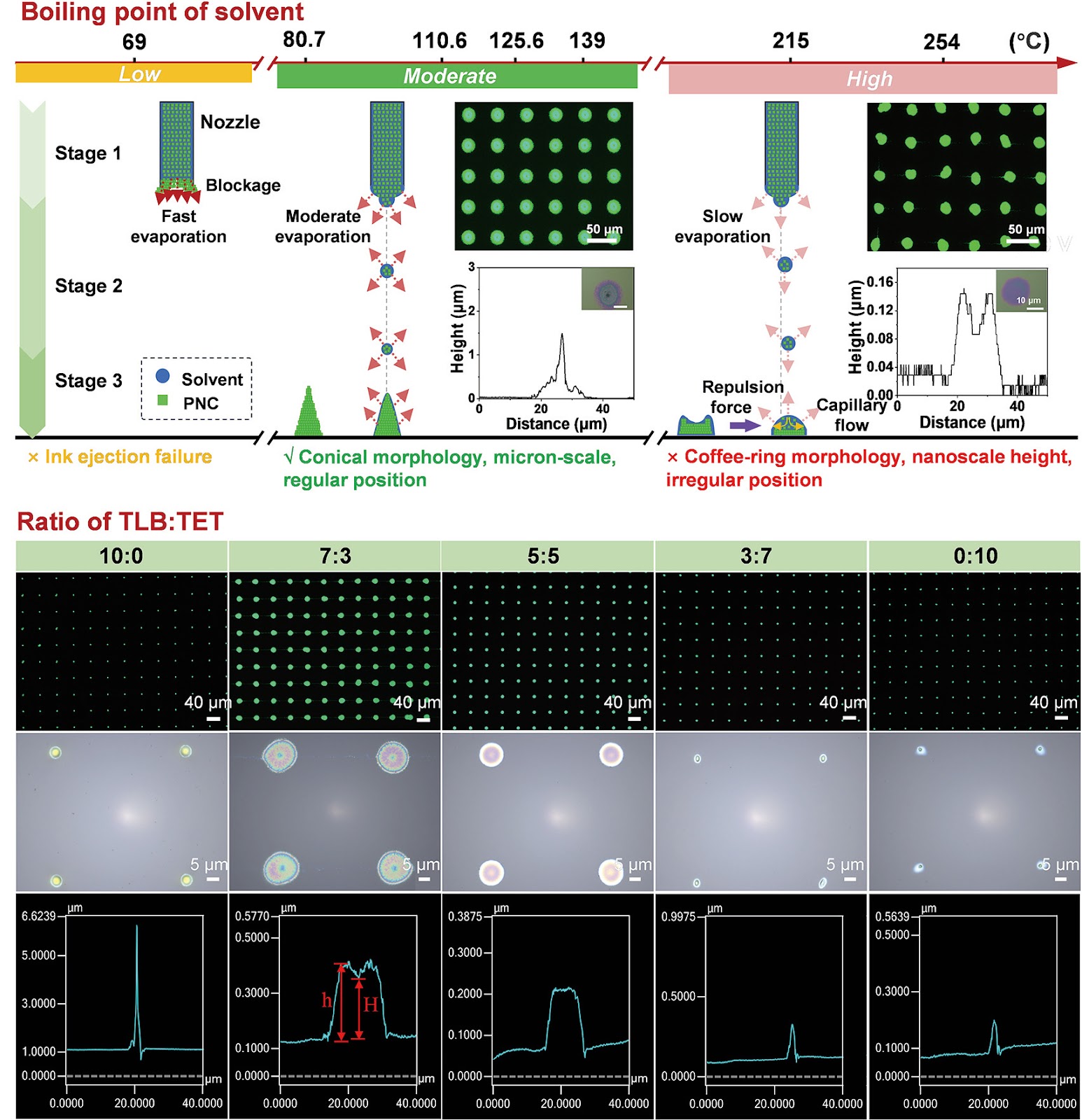
Electrohydrodynamic (EHD) inkjet printing has emerged as a powerful micro-/nanofabrication technique for high-resolution perovskite quantum dot (PeQD) color-conversion layers, offering precise control over pixel morphology, dimensions, and composition. This review systematically examines the mechanisms of cone-jet and electrostatic-attraction modes in EHD printing, highlighting recent advances in PeQD ink design, solvent and ligand engineering, and printing parameter optimization. Perovskite precursor and colloidal inks are discussed in detail, emphasizing strategies to enhance droplet ejection stability, suppress coffee-ring effects, and achieve uniform, high-luminescence pixels. Ligand exchange, dual-ligand passivation, and core−shell or polymer encapsulation are shown to effectively mitigate ion migration, surface defects, and environmental degradation, thereby improving photoluminescence efficiency and stability. Multi-channel and multi-nozzle EHD printing systems enable dynamic halide composition control and parallel RGB pixel deposition, facilitating ultrahigh-resolution patterning down to submicron feature sizes. Finally, the review highlights future directions, including synergistic PeQD material synthesis, advanced ink formulation, scalable high-throughput printing, and integration of PeQD color-conversion pixels into full-color micro-LED displays with minimal crosstalk and robust operational stability. These developments collectively demonstrate the immense potential of EHD inkjet printing for next-generation high-performance display technologies.

Electrohydrodynamic Inkjet Printing of Perovskite Quantum Dots for Color-Conversion Micro-LED Displays
Graphical Abstract
Original ResearchVol. 32, Issue 12 • pp. 100-112DOI: 10.1088/1674-4926/25120042Jan 15, 2025

Room-Temperature Electrically Injected GaN-Based Vertical-Cavity Surface-Emitting Laser with Conductive Nanoporous Distributed Bragg Reflector

Authors: Chuanjie Li, Meixin Feng, Jianping Liu, Aiqin Tian, Xuan Li, Wei Zhou, Rui Xi, Shuming Zhang, Qian Sun, Hui Yang

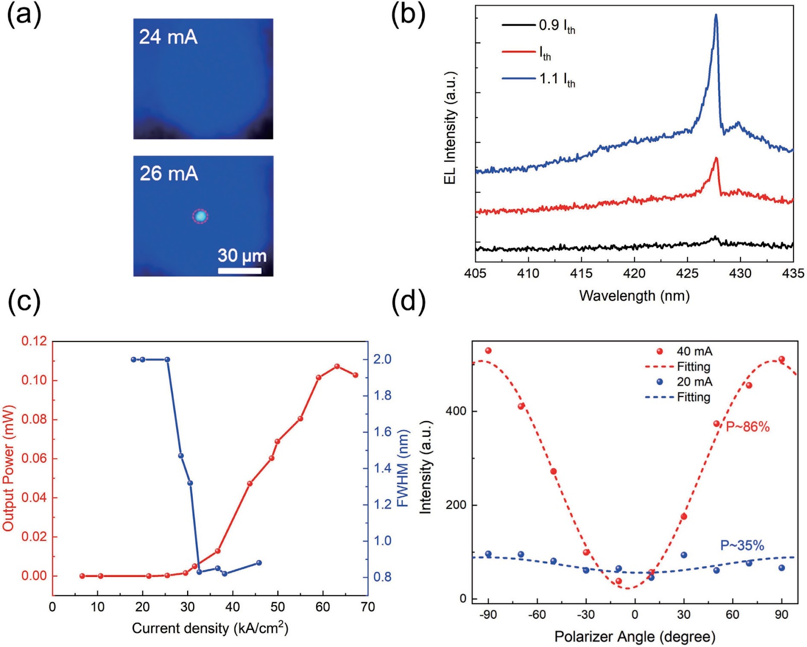
Vertical-cavity surface-emitting lasers (VCSELs) offer numerous advantages, including the ability to form two-dimensional arrays, low power consumption, and easy coupling, making them promising for visible-light communication, sensing, and micro-display applications. In GaAs-based VCSELs, conductive epitaxial semiconductor distributed Bragg reflectors (DBRs) enable straightforward vertical current injection. However, in GaN-based VCSELs, the lack of p-type conductive epitaxial DBRs has necessitated complex fabrication processes, such as flip-chip bonding and substrate thinning, which increase thermal resistance and reduce yield. In this work, we demonstrate a room-temperature electrically injected GaN-based VCSEL employing a conductive nanoporous (NP) GaN DBR. The NP-GaN DBR, fabricated by electrochemical etching of highly Si-doped n+-GaN layers, exhibits a high reflectivity of 99.9% with a stopband width of about 35 nm, while retaining excellent electrical conductivity. The device structure incorporates a 10λ cavity for enhanced lateral heat dissipation, a 10-μm-diameter current aperture, and a top dielectric DBR with reduced reflectivity (99.2%) to facilitate top emission. The vertical series resistance through the NP-GaN DBR is approximately 4.5 Ω, significantly lower than that of AlInN/GaN DBRs (>60 Ω), demonstrating the superior electrical performance of the NP-GaN DBR. This work presents a promising approach for achieving high-performance GaN-based VCSELs with simplified fabrication and improved thermal management, paving the way for their integration into high-density display and communication systems.

Room-Temperature Electrically Injected GaN-Based Vertical-Cavity Surface-Emitting Laser with Conductive Nanoporous Distributed Bragg Reflector
Graphical Abstract
Original ResearchVol. 32, Issue 12 • pp. 100-112DOI: 10.1088/1674-4926/25120050Jan 15, 2025

Electrochromic Retina E-Paper: Defining the Ultimate Display at the Human Vision Limit

Authors: Tongqing Zhou, Jianmin Li, Shujuan Liu, Qiang Zhao

In an era dominated by visual information, the display interface serves as a critical gateway between the human and digital worlds. The relentless pursuit of visual immersion has driven display technology from cinema screens to smartphones and now to virtual and augmented reality (VR/AR) headsets, progressively moving closer to the human eye. This evolution places unprecedented demands on pixel density, power efficiency, and form factor, pushing up against fundamental physical and physiological limits. The core challenge lies in creating displays that, when viewed at close proximity, offer a seamless, high-fidelity visual experience indistinguishable from reality—a goal often conceptualized as the 'retina display', where the pixel density matches or exceeds the resolving power of the human eye. However, as pixel sizes shrink into the sub-micrometer regime, conventional emissive technologies like organic light-emitting diodes (OLEDs) and micro-light-emitting diodes (micro-LEDs) face insurmountable hurdles: diminished emission intensity, non-uniformity, severe colour cross-talk, and rapidly increasing fabrication complexity. Even the most advanced micro-LED demonstrations struggle to achieve the required pixel densities across large fields of view without significant performance trade-offs. Conversely, reflective displays, or electronic paper (E-paper), which leverage ambient light for visibility, inherently avoid the luminosity and efficiency issues of emissive displays. Their optical contrast is governed by material properties at the nanoscale, remaining theoretically unaffected by pixel size reduction. Yet, established reflective technologies, such as electrophoretic displays (e.g., those in e-readers), have been hamstrung by slow refresh rates (seconds), limited colour gamuts, and resolutions typically below 1000 pixels per inch (PPI), confining them largely to static text and image applications. While optical metasurfaces have demonstrated astonishing static resolutions exceeding 10 000 PPI, they have largely remained just that—static—lacking the dynamic tunability essential for video and interactive content. Previous attempts to create dynamic reflective displays using hybrid nanomaterials have improved colour and speed but failed to break the micron-scale pixel barrier, leaving the holy grail of a high-resolution, video-rate, low-power reflective display tantalizingly out of reach. Now, writing in Nature, Santosa et al. achieve a retina E-paper that not only surmounts these historical limitations but also redefines the possibilities for ultra-high-resolution displays, based on traditional electrochromic (EC) technology. By demonstrating electrically tunable pixels down to ~560 nm in size (>25 000 PPI), full-colour video capability (>25 Hz), high reflectance (~80%), and remarkably low energy consumption (0.5–1.7 mW∙cm–2), they present a paradigm shift from light-emitting to intelligently light-modulating displays at the nanoscale.
Electrochromic Retina E-Paper: Defining the Ultimate Display at the Human Vision Limit
Graphical Abstract