Key Takeaways & Executive Findings
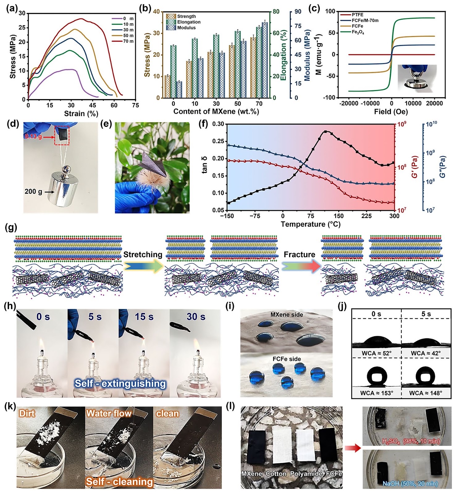
- •• The Janus-type multifunctional ultra-flexible polytetrafluoroethylene-carbon nanotube-Fe3O4/MXene (FCFe/M) membranes were fabricated via a shear-induced in situ fibrillation technique followed by vacuum-assisted filtration. • Thanks to the strategic distribution of the MXene conductive reflection layer and the silk-like FCFe electromagnetic wave’s absorption layer, the membranes achieve robust electromagnetic interference shielding and effective antireflection through the absorption-reflection-reabsorption mechanism. • The membranes exhibit exceptional thermal management performance, including efficient heat dissipation and electrothermal/photothermal conversion capabilities, further enhancing their promising potential for applications in flexible wearable technologies. • The FCFe/M membrane with a thickness of only 84.9 µm delivers outstanding EMI shielding effectiveness of 44.56 dB in the X-band, with a normalized specific SE reaching 10,421.3 dB cm2 g−1, and can reach surface temperatures up to 140.4 °C and 145.7 °C under 3 V voltage and 320 mW cm−2 optical power density, respectively.
Abstract
Herein, a novel Janus-structured multifunctional membrane with integrated electromagnetic interference (EMI) shielding and personalized thermal management is fabricated using shear-induced in situ fibrillation and vacuum-assisted filtration. Interestingly, within the polytetrafluoroethylene (PTFE)-carbon nanotube (CNT)-Fe3O4 layer (FCFe), CNT nanofibers interweave with PTFE fibers to form a stable “silk-like” structure that effectively captures Fe3O4 particles. By incorporating a highly conductive MXene layer, the FCFe/MXene (FCFe/M) membrane exhibits excellent electrical/thermal conductivity, mechanical properties, and flame retardancy. Impressively, benefiting from the rational regulation of component proportions and the design of a Janus structure, the FCFe/M membrane with a thickness of only 84.9 µm delivers outstanding EMI shielding effectiveness of 44.56 dB in the X-band, with a normalized specific SE reaching 10,421.3 dB cm2 g−1, which is attributed to the “absorption-reflection-reabsorption” mechanism. Furthermore, the membrane demonstrates low-voltage-driven Joule heating and fast-response photothermal performance. Under the stimulation of a 3 V voltage and an optical power density of 320 mW cm−2, the surface temperatures of the FCFe/M membranes can reach up to 140.4 and 145.7 °C, respectively. In brief, the FCFe/M membrane with anti-electromagnetic radiation and temperature regulation is an attractive candidate for the next generation of wearable electronics, EMI compatibility, visual heating, thermotherapy, and military and aerospace applications.
1. Introduction
With the rapid advancement of modern electronic devices, electromagnetic interference (EMI) has become a critical concern, necessitating the development of efficient shielding materials. However, conventional EMI shielding materials often suffer from high reflectivity, leading to secondary electromagnetic pollution. Therefore, there is a pressing need for a multifunctional and innovative design that integrates robust shielding and effective antireflection with thin and flexible characteristics.
A rational approach to resolve this paradox is to tailor the local conductivity of materials to fulfill varying requirements, by strategically positioning optimized compositions and architectures in appropriate regions, thereby integrating antireflective and shielding structures within a single asymmetric material. Grounded in impedance matching theory, constructing multilayer materials featuring a continuous conductivity gradient offers the potential for near-perfect antireflective EMI shielding. Despite this approach being conceptually straightforward, the intricate layer-by-layer fabrication process and the weak interlayer interactions substantially compromise the overall material performance. Therefore, developing a simpler and more feasible approach to fabricate asymmetric structures with superior performance remains a significant challenge.
Recently, Janus-structured materials have garnered widespread attention due to their unique asymmetric structure and straightforward fabrication process. In comparison to conventional homogeneous materials, Janus structures possess distinctly different chemical compositions and microstructures on each side, enabling them to exhibit superior multifunctional performance through asymmetric synergistic effects and independent mechanisms. Particularly in the field of EMI shielding, designing one side of the material as an EMW reflective layer composed of high-conductivity materials, and the other side as an EMW absorbing layer based on CPCs can induce an “absorb-reflect-reabsorb” EMI shielding mechanism, which effectively shields EMWs while minimizing reflection effects.
Loading authentic research manuscript (Pages 1–5)...
Runze Shao, Guilong Wang, Jialong Chai, Jun Lin, Guoqun Zhao, Zhihui Zeng, Guizhen Wang (2025). Multifunctional Janus-Structured Polytetrafluoroethylene-Carbon Nanotube-Fe3O4/MXene Membranes for Enhanced EMI Shielding and Thermal Management. Nano-Micro Letters. https://doi.org/10.1007/s40820-025-01647-x
Research & Educational Purpose Only:The translations, structured abstracts, analytical annotations, and data reports provided by SinoTechIntel are intended exclusively for academic research, internal corporate R&D, and educational benchmarking. They do not constitute formal engineering, chemical safety, legal, or professional advice.
Copyright & Intellectual Property Notice: Original copyright of the underlying source articles and experimental data remains with the respective authors, institutions, and original publishing journals. SinoTechIntel claims intellectual property only over its proprietary translations, analytical syntheses, and AEO structured enhancements in accordance with international fair use and academic citation principles.
Frequently Asked Questions
What is the main innovation of this study?
The study presents a novel Janus-structured membrane integrating a conductive MXene layer and a silk-like FCFe absorption layer, achieving enhanced EMI shielding and thermal management in a thin, flexible form.
How does the Janus structure contribute to EMI shielding?
The Janus structure enables an 'absorption-reflection-reabsorption' mechanism, where the MXene layer reflects electromagnetic waves and the FCFe layer absorbs them, reducing reflection and enhancing overall shielding effectiveness.
What are the key performance metrics of the FCFe/M membrane?
The membrane exhibits an EMI shielding effectiveness of 44.56 dB in the X-band with a thickness of only 84.9 µm, and a normalized specific SE of 10,421.3 dB cm2 g−1. It also shows excellent Joule heating and photothermal conversion, reaching temperatures up to 140.4 °C and 145.7 °C under 3 V and 320 mW cm−2, respectively.
What are the potential applications of this membrane?
The membrane is suitable for flexible wearable electronics, EMI compatibility, visual heating, thermotherapy, and military and aerospace applications due to its combined shielding and thermal management capabilities.
How is the FCFe/M membrane fabricated?
The membrane is fabricated via a shear-induced in situ fibrillation technique followed by vacuum-assisted filtration, which allows for the formation of a stable silk-like structure and the strategic distribution of components.
Related Technical Papers & Translations
Direct Repair of the Crystal Structure and Coating Surface of Spent LiFePO4 Materials Enables Superfast Li-Ion Migration
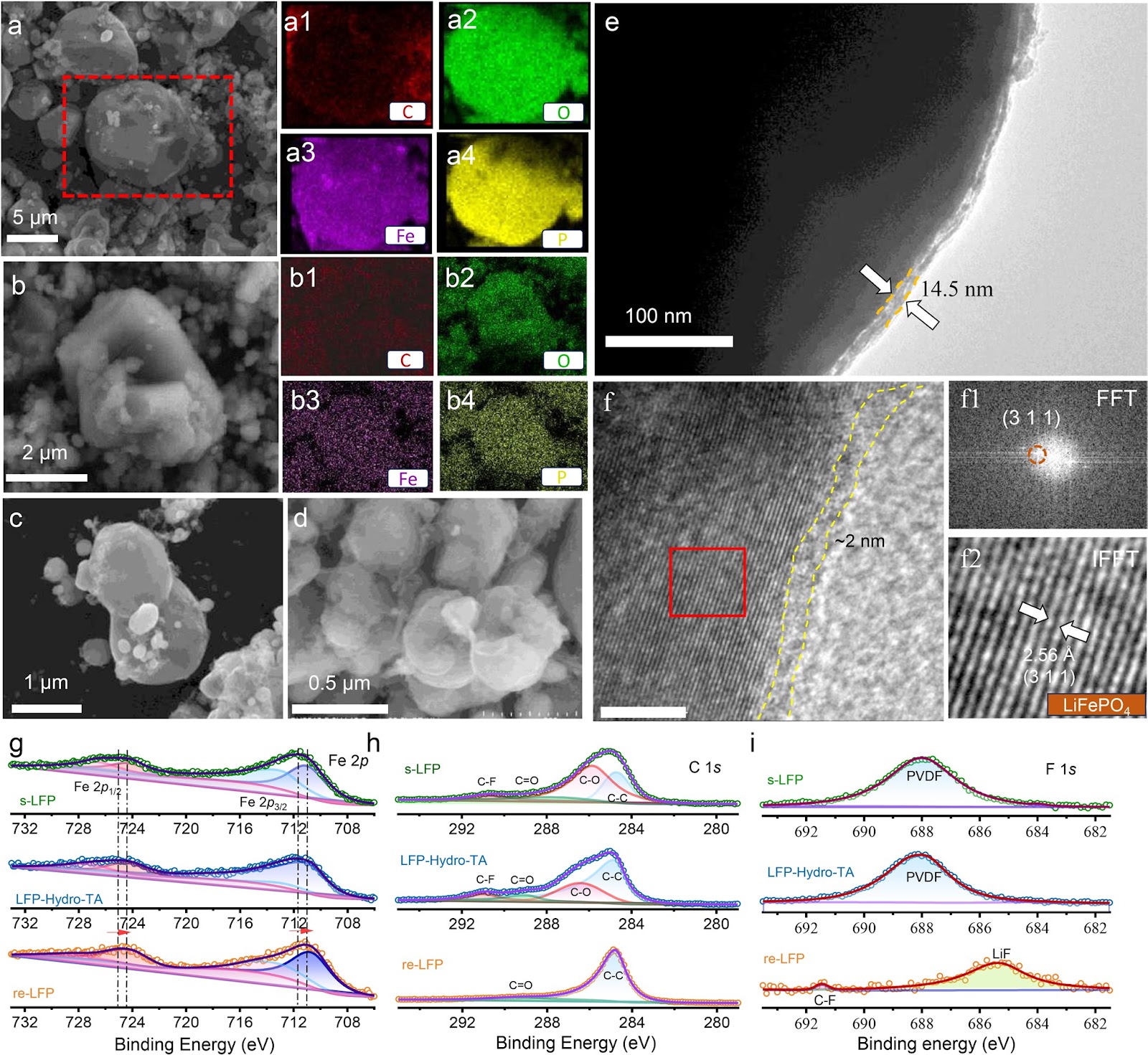
The rapid accumulation of spent LiFePO4 (LFP) cathodes from retired lithium-ion batteries necessitates the development of effective and environmental-friendly recycling strategies. In this context, direct regeneration has emerged as a promising approach for reclaiming LFP cathode materials, offering a streamlined pathway to restore their electrochemical functionality. We report an integrated regeneration protocol that simultaneously repairs the degraded crystal structure and reconstructs the damaged carbon coating in spent LFP. The regenerated cathode material had superfast lithium-ion diffusion kinetics and a stable cathode–electrolyte interface, giving a remarkable rate capability with specific capacities of 122 mAh g−1 at 5C and 106 mAh g−1 at 10C (1C = 170 mA g−1). It also maintained capacities of 110.7 mAh g−1 (5C) and 84.1 mAh g−1 (10C) after 400 cycles. It could be used in harsh environments and could be stably cycled at subzero temperatures (−10 and −20 °C) and in solid-state electrolyte batteries. Life cycle assessment combined with economic evaluation using the EverBatt model reveals that this direct regeneration approach has high economic and environmental benefits.
Oxide Semiconductor for Advanced Memory Architectures: Atomic Layer Deposition, Key Requirement and Challenges
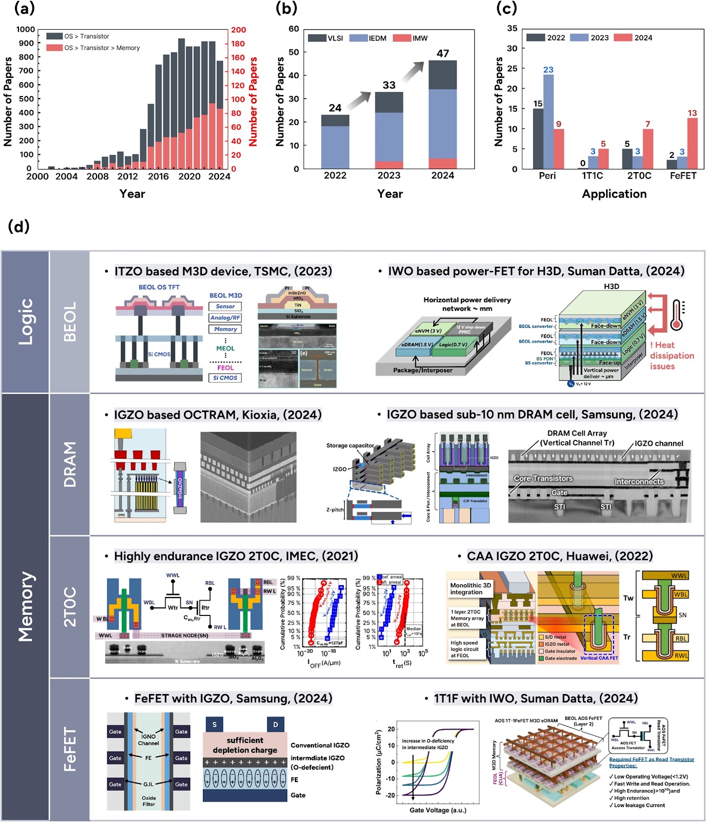
Oxide semiconductors (OSs), introduced by the Hosono group in the early 2000s, have evolved from display backplane materials to promising candidates for advanced memory and logic devices. The exceptionally low leakage current of OSs and compatibility with three-dimensional (3D) architectures have recently sparked renewed interest in their use in semiconductor applications. This review begins by exploring the unique material properties of OSs, which fundamentally originate from their distinct electronic band structure. Subsequently, we focus on atomic layer deposition (ALD), a core technique for growing excellent OS films, covering both basic and advanced processes compatible with 3D scaling. The basic surface reaction mechanisms—adsorption and reaction—and their roles in film growth are introduced. Furthermore, material design strategies, such as cation selection, crystallinity control, anion doping, and heterostructure engineering, are discussed. We also highlight challenges in memory applications, including contact resistance, hydrogen instability, and lack of p-type materials, and discuss the feasibility of ALD-grown OSs as potential solutions. Lastly, we provide an outlook on the role of ALD-grown OSs in memory technologies. This review bridges material fundamentals and device-level requirements, offering a comprehensive perspective on the potential of ALD-driven OSs for next-generation semiconductor memory devices.
Laser powder bed fusion of biodegradable Zn-4Cu alloy: Processing, microstructure and properties
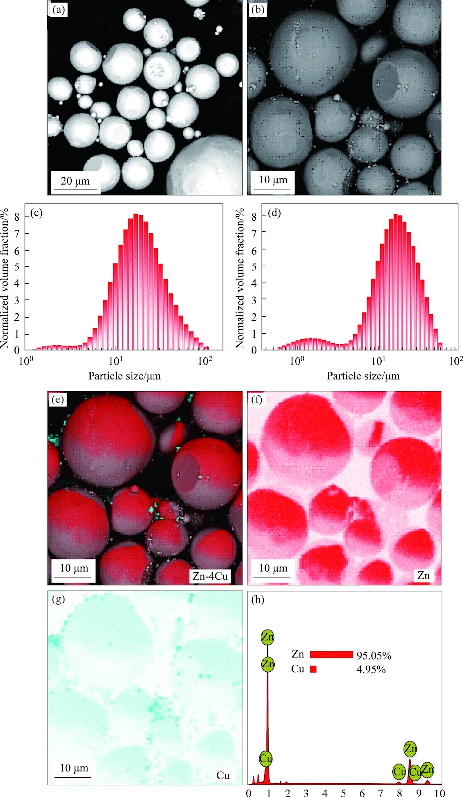
Zn's natural degradability and biocompatibility make it a promising candidate for implants, however, its mechanical properties remain insufficient for bone applications. In this study, the performance of Zn was enhanced by developing Zn-Cu alloys via laser powder bed fusion (LPBF). Optimal LPBF parameters for forming stable tracks were achieved by adjusting laser power and scanning speed. Under optimized conditions of 100 W and 100 mm/s, high-density (99.58%) Zn-Cu alloys with improved hardness (68.2HV) and yield strength (160 MPa) were achieved. These improvements are attributed to solid solution strengthening, segregation strengthening, and grain refinement. The Zn-Cu alloys also demonstrated favorable degradation behavior, with a rate of 0.16 mm/year. This degradation is primarily driven by micro-galvanic corrosion between the CuZn5 phase and Zn matrix, along with refined grains and increased grain boundary density. This work demonstrates a viable strategy for fabricating Zn-based implants with enhanced structural integrity and mechanical performance via LPBF.