Key Takeaways & Executive Findings
- •• Hand-printing on cellulose paper enables low-cost, scalable fabrication of flexible electronics without toxic solvents or sophisticated equipment. • Paper-based devices achieve competitive performance: photodetectors with responsivity up to 52 mA/W, supercapacitors with energy density ~15.1 mWh/cm2, and pressure sensors with sensitivity ~18.42 kPa−1. • Integration of functional nanomaterials (2D chalcogenides, metal oxides, conductive polymers, carbon structures) on paper enhances device functionality for energy harvesting, storage, and sensing. • This approach aligns with green technology and UN Sustainable Development Goals by reducing e-waste and promoting recyclable, biodegradable electronics.
Abstract
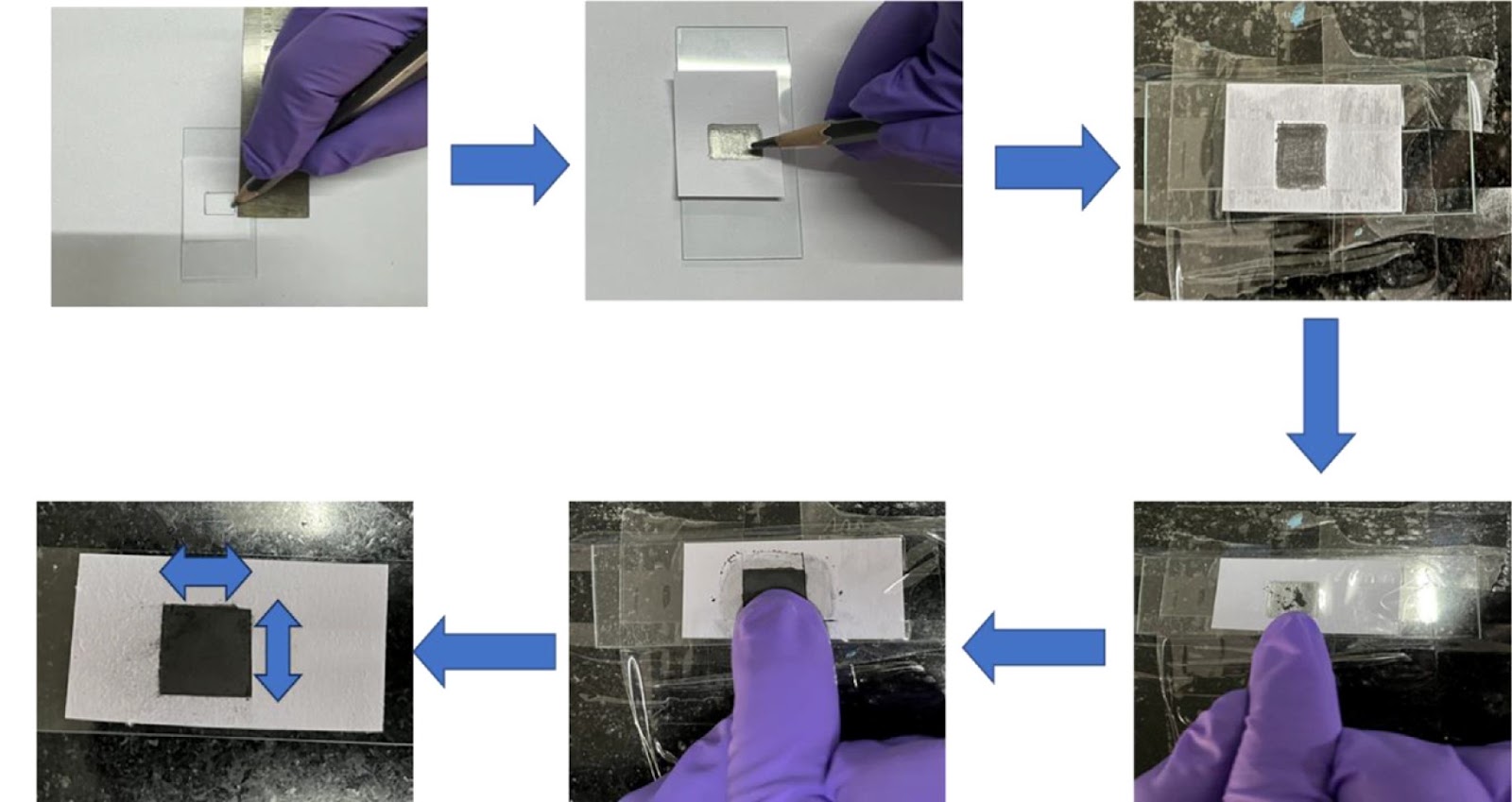
The rapid advancement of modern electronics has led to a surge in solid electronic waste, which poses significant environmental and health challenges. This review focuses on recent developments in paper-based electronic devices fabricated through low-cost, hand-printing techniques, with particular emphasis on their applications in energy harvesting, storage, and sensing. Unlike conventional plastic-based substrates, cellulose paper offers several advantages, including biodegradability, recyclability, and low fabrication cost. By integrating functional nanomaterials such as two-dimensional chalcogenides, metal oxides, conductive polymers, and carbon-based structures onto paper, researchers have achieved high-performance devices such as broadband photodetectors (responsivity up to 52 mA/W), supercapacitors (energy density ~15.1 mWh/cm2), and pressure sensors (sensitivity ~18.42 kPa−1). The hand-printing approach, which eliminates the need for sophisticated equipment and toxic solvents, offers a promising route for scalable, sustainable, and disposable electronics. This review outlines fabrication methods and key performance metrics, and discusses the current challenges and future directions for realizing robust, flexible devices aligned with green technology and the United Nation’s Sustainable Development Goals.
1. Introduction
Electronic solid waste contributes to pollution, resource depletion, and rising landfill demands, posing serious environmental problems worldwide [1]. These problems are exacerbated by the build-up of nonbiodegradable elements from abandoned devices, which cause long-term environmental damage. A key way to address these problems is to use recyclable materials and substrates in energy harvesting and conversion devices. The use of environment-friendly materials, such as cellulose paper (CP), can significantly slow down the increase in solid waste, which has advantages for the environment and economy [2]. The reduced use of nonrecyclable materials not only promotes sustainability but also aids in resource conservation, making it a good sustainable approach for emerging technologies [3].
Paper is an exceptional substrate for flexible and disposable devices, offering several advantages that align with the United Nations Sustainable Development Goals (SDGs) [4]. Paper is economical, biocompatible, environmentally benign, and 100% recyclable, unlike synthetic substitutes such as polyethylene terephthalate, polyimide, and other polymer-based substrates [5–6]. In addition, the elastic and lightweight qualities of paper make it ideal for disposable, wearable, and portable electronics, which advances the SDG industry, innovation, and infrastructure by facilitating the creation of flexible and economically viable technology [2,7]. Paper-based devices promote affordable and clean energy applications, such as photodetectors [8], solar cells [9], supercapacitors (SCs) [10], and paper-based batteries [11].
Loading authentic research manuscript (Pages 1–5)...
Parth Shah, Sanjay A. Bhakhar, Pratik M. Pataniya, C.K. Sumesh (2025). Hand-printed paper-based devices: Toward green flexible electronics and sensing applications. Int. Journal of Minerals, Metallurgy and Materials (矿物冶金与材料学报). https://doi.org/10.1007/s12613-025-3220-9
Research & Educational Purpose Only:The translations, structured abstracts, analytical annotations, and data reports provided by SinoTechIntel are intended exclusively for academic research, internal corporate R&D, and educational benchmarking. They do not constitute formal engineering, chemical safety, legal, or professional advice.
Copyright & Intellectual Property Notice: Original copyright of the underlying source articles and experimental data remains with the respective authors, institutions, and original publishing journals. SinoTechIntel claims intellectual property only over its proprietary translations, analytical syntheses, and AEO structured enhancements in accordance with international fair use and academic citation principles.
Frequently Asked Questions
What are the main advantages of using paper as a substrate for flexible electronics?
Paper offers several advantages including biodegradability, recyclability, low cost, biocompatibility, and lightweight properties, making it an ideal substrate for disposable and wearable electronics, aligning with green technology and sustainability goals.
How does the hand-printing technique contribute to sustainable electronics?
The hand-printing technique eliminates the need for sophisticated equipment and toxic solvents, enabling low-cost, scalable fabrication of paper-based devices, thus reducing environmental impact and promoting sustainable manufacturing.
What performance metrics are highlighted for paper-based photodetectors?
The review highlights photodetectors with responsivity up to 52 mA/W, along with other metrics such as detectivity, external quantum efficiency, and response time, demonstrating competitive performance for sensing applications.
Which nanomaterials are integrated onto paper for enhanced device performance?
Functional nanomaterials such as two-dimensional chalcogenides, metal oxides, conductive polymers, and carbon-based structures are integrated onto paper to achieve high-performance devices for energy harvesting, storage, and sensing.
How do paper-based devices align with the United Nations Sustainable Development Goals?
Paper-based devices promote affordable and clean energy, industry innovation, and infrastructure, and contribute to reducing e-waste, thus supporting several SDGs including those related to responsible consumption and production, and climate action.
Related Technical Papers & Translations
Direct Repair of the Crystal Structure and Coating Surface of Spent LiFePO4 Materials Enables Superfast Li-Ion Migration
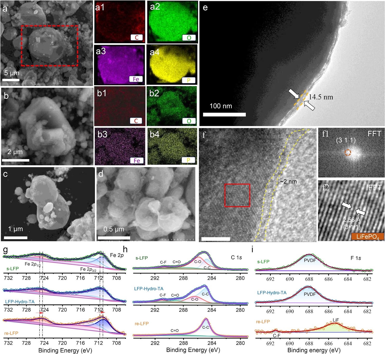
The rapid accumulation of spent LiFePO4 (LFP) cathodes from retired lithium-ion batteries necessitates the development of effective and environmental-friendly recycling strategies. In this context, direct regeneration has emerged as a promising approach for reclaiming LFP cathode materials, offering a streamlined pathway to restore their electrochemical functionality. We report an integrated regeneration protocol that simultaneously repairs the degraded crystal structure and reconstructs the damaged carbon coating in spent LFP. The regenerated cathode material had superfast lithium-ion diffusion kinetics and a stable cathode–electrolyte interface, giving a remarkable rate capability with specific capacities of 122 mAh g−1 at 5C and 106 mAh g−1 at 10C (1C = 170 mA g−1). It also maintained capacities of 110.7 mAh g−1 (5C) and 84.1 mAh g−1 (10C) after 400 cycles. It could be used in harsh environments and could be stably cycled at subzero temperatures (−10 and −20 °C) and in solid-state electrolyte batteries. Life cycle assessment combined with economic evaluation using the EverBatt model reveals that this direct regeneration approach has high economic and environmental benefits.
Oxide Semiconductor for Advanced Memory Architectures: Atomic Layer Deposition, Key Requirement and Challenges
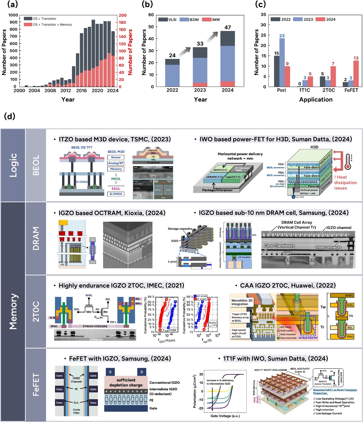
Oxide semiconductors (OSs), introduced by the Hosono group in the early 2000s, have evolved from display backplane materials to promising candidates for advanced memory and logic devices. The exceptionally low leakage current of OSs and compatibility with three-dimensional (3D) architectures have recently sparked renewed interest in their use in semiconductor applications. This review begins by exploring the unique material properties of OSs, which fundamentally originate from their distinct electronic band structure. Subsequently, we focus on atomic layer deposition (ALD), a core technique for growing excellent OS films, covering both basic and advanced processes compatible with 3D scaling. The basic surface reaction mechanisms—adsorption and reaction—and their roles in film growth are introduced. Furthermore, material design strategies, such as cation selection, crystallinity control, anion doping, and heterostructure engineering, are discussed. We also highlight challenges in memory applications, including contact resistance, hydrogen instability, and lack of p-type materials, and discuss the feasibility of ALD-grown OSs as potential solutions. Lastly, we provide an outlook on the role of ALD-grown OSs in memory technologies. This review bridges material fundamentals and device-level requirements, offering a comprehensive perspective on the potential of ALD-driven OSs for next-generation semiconductor memory devices.
Laser powder bed fusion of biodegradable Zn-4Cu alloy: Processing, microstructure and properties
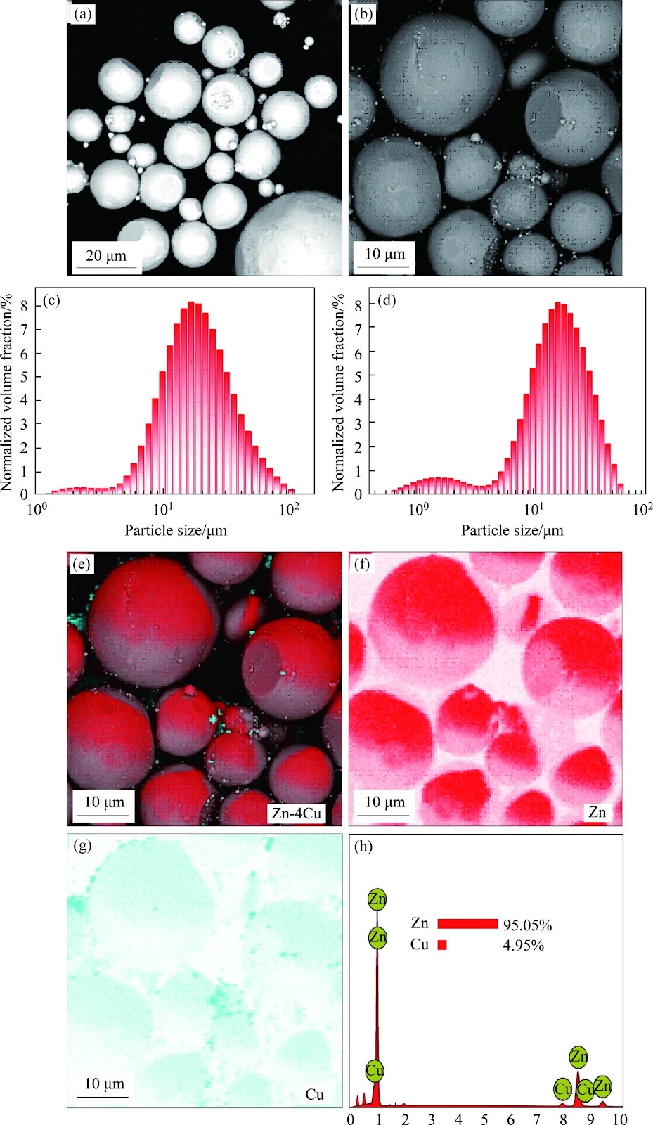
Zn's natural degradability and biocompatibility make it a promising candidate for implants, however, its mechanical properties remain insufficient for bone applications. In this study, the performance of Zn was enhanced by developing Zn-Cu alloys via laser powder bed fusion (LPBF). Optimal LPBF parameters for forming stable tracks were achieved by adjusting laser power and scanning speed. Under optimized conditions of 100 W and 100 mm/s, high-density (99.58%) Zn-Cu alloys with improved hardness (68.2HV) and yield strength (160 MPa) were achieved. These improvements are attributed to solid solution strengthening, segregation strengthening, and grain refinement. The Zn-Cu alloys also demonstrated favorable degradation behavior, with a rate of 0.16 mm/year. This degradation is primarily driven by micro-galvanic corrosion between the CuZn5 phase and Zn matrix, along with refined grains and increased grain boundary density. This work demonstrates a viable strategy for fabricating Zn-based implants with enhanced structural integrity and mechanical performance via LPBF.