Key Takeaways & Executive Findings
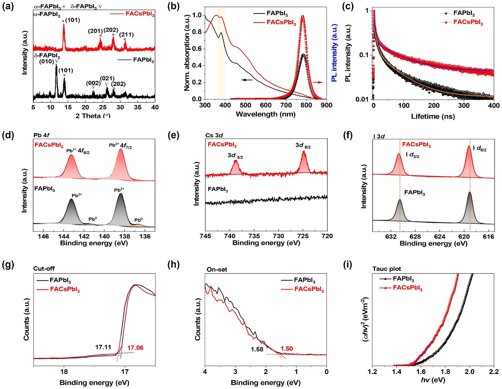
- •• α-phase formamidinium lead triiodide (FAPbI3) was prepared based on triple-source co-evaporation. • A partial Cs-doping in the FAPbI3 can help with the suppression of the non-radiative recombination, elimination of the metallic Pb, improvement of spatial confinement. • Near-infrared perovskite light-emitting diodes (NIR-PeLEDs) based on triple-source co-evaporated FACsPbI3 thin films achieved a maximum external quantum efficiency of 10.25%, which was around 6 times higher than that of FAPbI3-based NIR-PeLEDs. • The work demonstrates a reliable and effective strategy to achieve α-FAPbI3 via thermal evaporation, paving the way toward highly efficient perovskite optoelectronic devices for future commercialization.
Abstract
α-phase formamidinium lead triiodide (FAPbI3) has demonstrated extraordinary properties for near-infrared perovskite light-emitting diodes (NIR-PeLEDs). The vacuum processing technique has recently received increasing attention from industry and academia due to its solvent-free feature and compatibility with large-scale production. Nevertheless, vacuum-deposited NIR-PeLEDs have been less studied, and their efficiencies lag far behind those of solution-based PeLEDs as it is still challenging to prepare pure α-FAPbI3 by the thermal evaporation. Herein, we report a Cs-containing triple-source co-evaporation approach to develop the perovskite films. The addition of thermally stable Cs cation fills in the perovskite crystal lattice and eliminates the formation of metallic Pb caused by the degradation of FA cation during the evaporation process. The tri-source co-evaporation strategy significantly promotes the phase transition from yellow δ-phase FAPbI3 to black α-phase FACsPbI3, fostering smooth, uniform, and pinhole-free perovskite films with higher crystallinity and fewer defects. On this basis, the resulting NIR-PeLED based on FACsPbI3 yields a maximum EQE of 10.25%, which is around sixfold higher than that of FAPbI3-based PeLEDs. Our work demonstrates a reliable and effective strategy to achieve α-FAPbI3 via thermal evaporation and paves the pathway toward highly efficient perovskite optoelectronic devices for future commercialization.
1. Introduction
Metal halide perovskites have rapidly emerged as a revolutionary frontier in display and lighting owing to their fascinating properties including high color purity, excellent charge transport properties, tunable chromaticity, and cost-effectiveness [1–5]. Specially, near-infrared perovskite light-emitting diodes (NIR-PeLEDs) hold great potential for a variety of applications such as medical treatment, data storage, optical communications, hyperspectral imaging, night vision for surveillance, and automotive safety [6, 7]. With tremendous efforts of researchers, the external quantum efficiencies (EQEs) of NIR-PeLEDs have exceeded 23% within the last few years [2, 4], enabling them to be a strong competitor of the III-V NIR-LEDs.
Up to date, the fabrication of formamidinium-based emitters such as FAPbI3 was regarded as the most successful approach to develop NIR-PeLEDs [2, 4, 7–9]. Nevertheless, most of the reported state-of-the-art NIR-PeLEDs were prepared via solution-based spin-coating, limiting their application in large-scale production. Inspired by the deposition of commercialized organic light-emitting diodes (OLEDs), thermal evaporation has been proposed as an alternative and effective technique to develop scalable PeLEDs [10]. Unlike solution-processing techniques, thermal evaporation can effectively avoid the problem of low solubility of some perovskite precursors. Besides, it can prevent the utilization of environmentally unfriendly organic solvents such as dimethylformamide (DMF) and dimethyl sulfoxide (DMSO). Furthermore, the process of thermal evaporation can be uniformly fabricated onto various substrates, paving a novel pathway for the heterogeneous integration of NIR-PeLEDs. Most importantly, thermal evaporation is compatible with the currently available OLED industry, thus lowering the initial investment and speeding up the commercialization of PeLEDs [3, 10–13].
Loading authentic research manuscript (Pages 1–5)...
Siwei He, Lanxin Qin, Zhengzheng Liu, Jae-Wook Kang, Jiajun Luo, Juan Du (2025). Efficient Thermally Evaporated Near-Infrared Perovskite Light-Emitting Diodes via Phase Regulation. Nano-Micro Letters. https://doi.org/10.1007/s40820-025-01776-3
Research & Educational Purpose Only:The translations, structured abstracts, analytical annotations, and data reports provided by SinoTechIntel are intended exclusively for academic research, internal corporate R&D, and educational benchmarking. They do not constitute formal engineering, chemical safety, legal, or professional advice.
Copyright & Intellectual Property Notice: Original copyright of the underlying source articles and experimental data remains with the respective authors, institutions, and original publishing journals. SinoTechIntel claims intellectual property only over its proprietary translations, analytical syntheses, and AEO structured enhancements in accordance with international fair use and academic citation principles.
Frequently Asked Questions
What is the main achievement of this paper?
The paper reports a triple-source co-evaporation method to prepare α-phase FAPbI3 films with partial Cs doping, achieving a maximum external quantum efficiency of 10.25% in near-infrared perovskite light-emitting diodes, which is about six times higher than that of pure FAPbI3-based devices.
Why is thermal evaporation advantageous for perovskite LED fabrication?
Thermal evaporation is solvent-free, avoids the use of toxic organic solvents, allows uniform deposition on various substrates, and is compatible with existing OLED manufacturing infrastructure, thus facilitating large-scale production and commercialization.
How does Cs doping improve the perovskite film quality?
Cs doping fills the perovskite crystal lattice, suppresses non-radiative recombination, eliminates metallic Pb formation, and promotes the phase transition from δ-phase to α-phase, resulting in smoother, more uniform, and pinhole-free films with higher crystallinity and fewer defects.
What are the potential applications of NIR-PeLEDs?
NIR-PeLEDs have potential applications in medical treatment, data storage, optical communications, hyperspectral imaging, night vision for surveillance, and automotive safety.
What is the significance of achieving high EQE in thermally evaporated NIR-PeLEDs?
Achieving high EQE in thermally evaporated NIR-PeLEDs demonstrates that vacuum deposition can rival solution processing, paving the way for scalable and environmentally friendly manufacturing of high-performance perovskite optoelectronic devices.
Related Technical Papers & Translations
Direct Repair of the Crystal Structure and Coating Surface of Spent LiFePO4 Materials Enables Superfast Li-Ion Migration
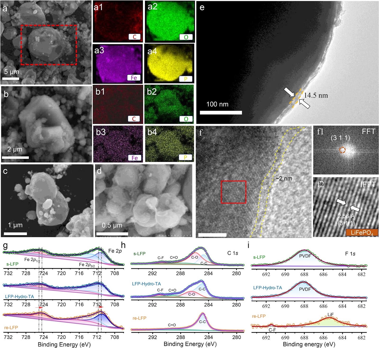
The rapid accumulation of spent LiFePO4 (LFP) cathodes from retired lithium-ion batteries necessitates the development of effective and environmental-friendly recycling strategies. In this context, direct regeneration has emerged as a promising approach for reclaiming LFP cathode materials, offering a streamlined pathway to restore their electrochemical functionality. We report an integrated regeneration protocol that simultaneously repairs the degraded crystal structure and reconstructs the damaged carbon coating in spent LFP. The regenerated cathode material had superfast lithium-ion diffusion kinetics and a stable cathode–electrolyte interface, giving a remarkable rate capability with specific capacities of 122 mAh g−1 at 5C and 106 mAh g−1 at 10C (1C = 170 mA g−1). It also maintained capacities of 110.7 mAh g−1 (5C) and 84.1 mAh g−1 (10C) after 400 cycles. It could be used in harsh environments and could be stably cycled at subzero temperatures (−10 and −20 °C) and in solid-state electrolyte batteries. Life cycle assessment combined with economic evaluation using the EverBatt model reveals that this direct regeneration approach has high economic and environmental benefits.
Oxide Semiconductor for Advanced Memory Architectures: Atomic Layer Deposition, Key Requirement and Challenges
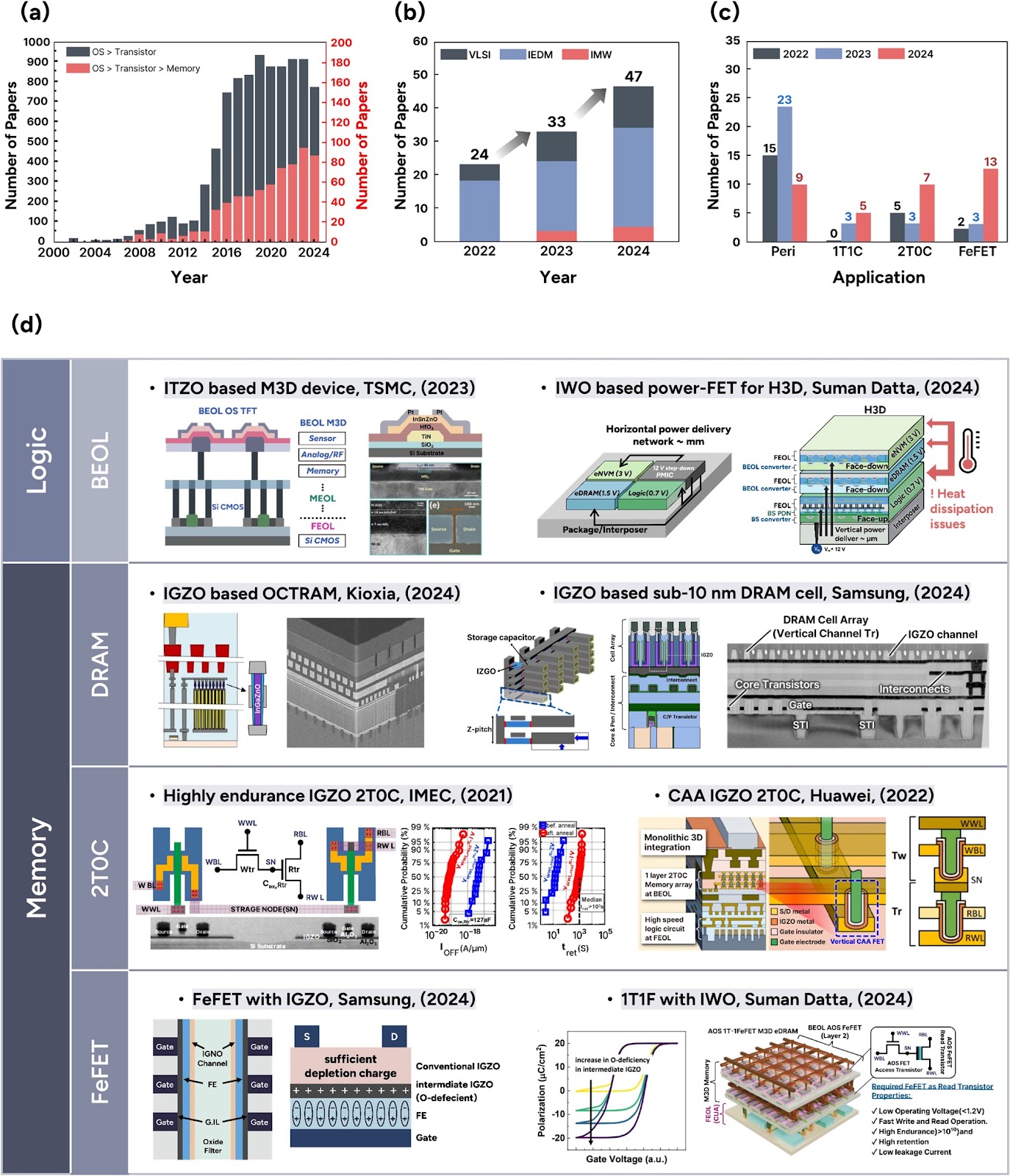
Oxide semiconductors (OSs), introduced by the Hosono group in the early 2000s, have evolved from display backplane materials to promising candidates for advanced memory and logic devices. The exceptionally low leakage current of OSs and compatibility with three-dimensional (3D) architectures have recently sparked renewed interest in their use in semiconductor applications. This review begins by exploring the unique material properties of OSs, which fundamentally originate from their distinct electronic band structure. Subsequently, we focus on atomic layer deposition (ALD), a core technique for growing excellent OS films, covering both basic and advanced processes compatible with 3D scaling. The basic surface reaction mechanisms—adsorption and reaction—and their roles in film growth are introduced. Furthermore, material design strategies, such as cation selection, crystallinity control, anion doping, and heterostructure engineering, are discussed. We also highlight challenges in memory applications, including contact resistance, hydrogen instability, and lack of p-type materials, and discuss the feasibility of ALD-grown OSs as potential solutions. Lastly, we provide an outlook on the role of ALD-grown OSs in memory technologies. This review bridges material fundamentals and device-level requirements, offering a comprehensive perspective on the potential of ALD-driven OSs for next-generation semiconductor memory devices.
Laser powder bed fusion of biodegradable Zn-4Cu alloy: Processing, microstructure and properties
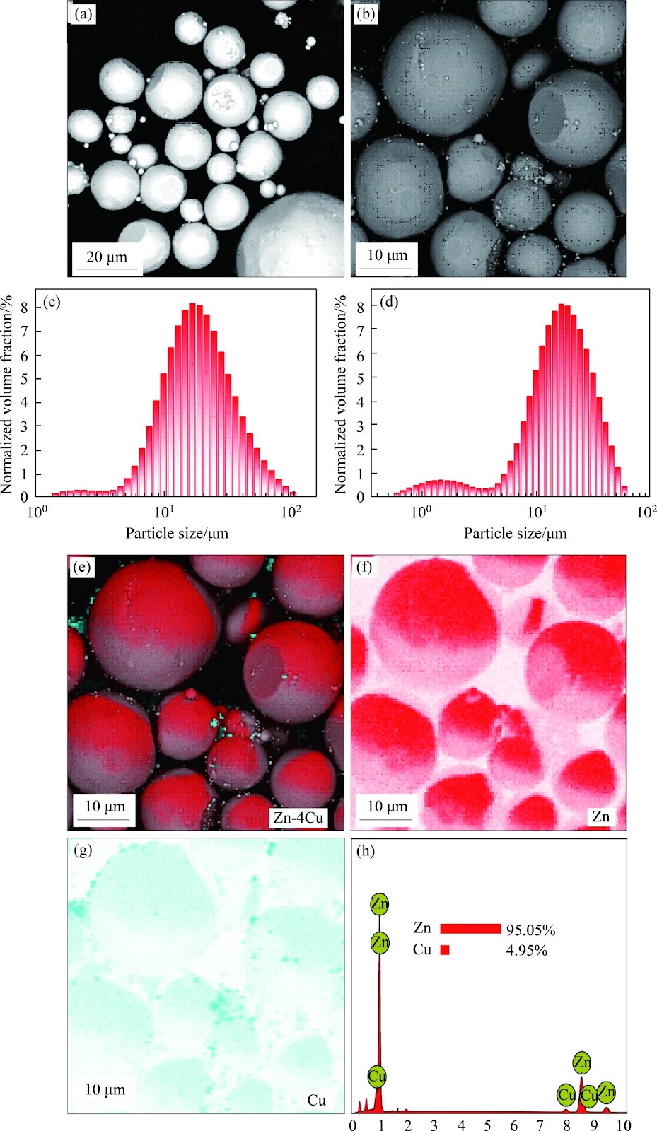
Zn's natural degradability and biocompatibility make it a promising candidate for implants, however, its mechanical properties remain insufficient for bone applications. In this study, the performance of Zn was enhanced by developing Zn-Cu alloys via laser powder bed fusion (LPBF). Optimal LPBF parameters for forming stable tracks were achieved by adjusting laser power and scanning speed. Under optimized conditions of 100 W and 100 mm/s, high-density (99.58%) Zn-Cu alloys with improved hardness (68.2HV) and yield strength (160 MPa) were achieved. These improvements are attributed to solid solution strengthening, segregation strengthening, and grain refinement. The Zn-Cu alloys also demonstrated favorable degradation behavior, with a rate of 0.16 mm/year. This degradation is primarily driven by micro-galvanic corrosion between the CuZn5 phase and Zn matrix, along with refined grains and increased grain boundary density. This work demonstrates a viable strategy for fabricating Zn-based implants with enhanced structural integrity and mechanical performance via LPBF.