SinoTechIntel Academic Portal
🏛️ Indexed Academic JournalImpact Factor: 3.8

Journal of Semiconductors (半导体学报 - 中国科学院半导体研究所)

Authoritative peer-reviewed journal in materials science, metallurgy, chemistry and engineering technologies: Journal of Semiconductors (半导体学报 - Viện Bán dẫn CAS)

Total Research Papers: 115
Access: 100% Free Open Access
Browse by Publication Year & VolumeReset All Filters ✕

Published Research PapersFiltered: Year 2025 • Vol. 32 • 11

Showing 3 of 115 peer-reviewed papers with full Graphical Abstracts.

Original ResearchVol. 32, Issue 11 • pp. 100-112DOI: 10.1088/1674-4926/25110013Jan 15, 2025

Advancing Highly Efficient and Mechanically Resilient Flexible Perovskite-Silicon Tandem Solar Cells

Authors: Zhaoyang Han, Qi Jiang

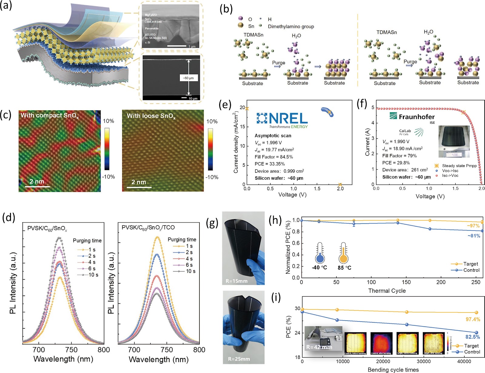
Perovskite-silicon tandem solar cells, combining high power conversion efficiency (PCE) with cost-effectiveness, are a leading direction for next-generation photovoltaics. In two-terminal tandems, a crystalline silicon (c-Si) bottom cell is series-connected with a wide-bandgap (1.65–1.7 eV) perovskite top cell, leveraging complementary spectral absorption to enhance sunlight harvesting. Rigid perovskite/c-Si tandems have achieved certified PCEs up to 34.9%, exceeding the Shockley–Queisser limit for single junctions. However, flexible perovskite-silicon tandems have lagged due to the intrinsic rigidity of c-Si, interfacial delamination under bending, and processing challenges. Recent breakthroughs in Nature report significant progress. One study by Zhang, Liu, and colleagues from Soochow University and LONGi Green Energy Technology developed a dual-buffer layer strategy using dense and loose SnOx layers formed by modulating ALD purge time. The dense layer ensures efficient charge extraction, while the loose layer acts as a cushion to relieve mechanical stress from TCO sputtering and bending. This architecture achieved a certified efficiency of 33.4% on 1 cm² and 29.8% on a wafer-scale module (~260 cm²), with a power-to-weight ratio of 1.77 W/g and bendability to 15 mm radius. These advances demonstrate the potential of flexible perovskite-silicon tandems for aerospace, wearable, and IoT applications, addressing key challenges in efficiency, flexibility, and durability.
Advancing Highly Efficient and Mechanically Resilient Flexible Perovskite-Silicon Tandem Solar Cells
Graphical Abstract
Original ResearchVol. 32, Issue 11 • pp. 100-112DOI: 10.1088/1674-4926/25110003Jan 15, 2025

Evolution of Diamond Film Growth Modes under Varied Plasma Conditions: Insights from Optical Emission Spectroscopy

Authors: Pengfei Qu, Guangdi Zhou, Peng Jin, Xu Han, Zhanguo Wang

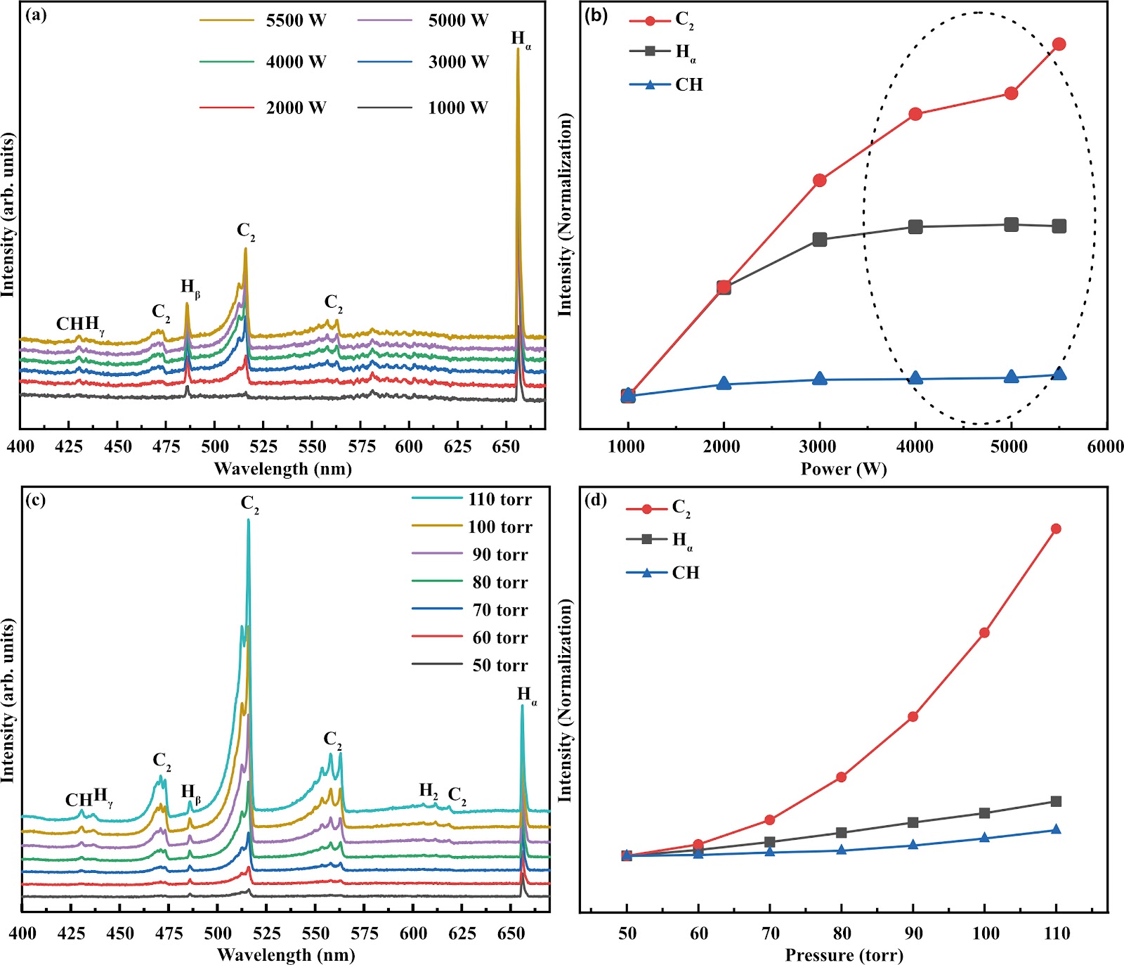
The synthesis of high-quality heteroepitaxial diamond films on iridium composite substrates is a critical step toward advancing diamond for electronic and optical applications. Microwave plasma chemical vapor deposition, combined with in situ optical emission spectroscopy, enables precise control over growth modes through plasma parameter tuning. In this study, we examine how methane concentration, microwave power, and gas pressure influence plasma species and, consequently, the growth modes of heteroepitaxial diamond by optical emission spectroscopy and scanning electron microscope. At low nucleation densities, increased methane concentrations promote the transition from faceted polyhedral to ballas structures, driven by elevated C2 radical concentrations in the plasma. Conversely, at higher nucleation densities, gas pressure, and substrate temperature dominate growth mode determination, leading to diverse morphologies, such as planar, polycrystalline, octahedral, and step-flow growth. These findings elucidate the interplay among plasma species, growth parameters, and growth mode, offering critical insights for optimizing growth conditions and preparing heteroepitaxial diamond films in a specific growth mode.

Evolution of Diamond Film Growth Modes under Varied Plasma Conditions: Insights from Optical Emission Spectroscopy
Graphical Abstract
Original ResearchVol. 32, Issue 11 • pp. 100-112DOI: 10.1088/1674-4926/25110004Jan 15, 2025

Realization of 193 nm DUV Laser through Direct Frequency Doubling with GaN-based UVA Laser Diode and ABF Crystal

Authors: Feng Liang, Fangfang Zhang, Jing Yang, Degang Zhao, Shilie Pan

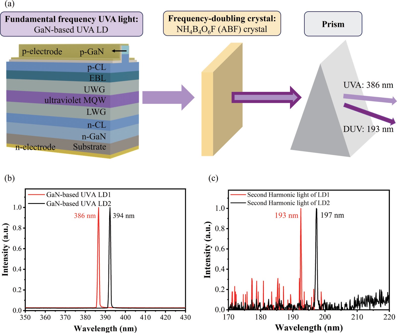
The 193 nm deep-ultraviolet (DUV) laser is crucial for advanced semiconductor manufacturing, micro-nano material characterization, and biomedical analysis due to its high spatial resolution and short wavelength. Currently, ArF excimer gas lasers dominate DUV lithography, but alternative approaches based on infrared solid-state lasers suffer from complexity and low efficiency. Direct frequency doubling of long-wavelength ultraviolet (UVA) semiconductor lasers using DUV nonlinear optical crystals offers a promising alternative. However, practical implementation has been challenging due to limited availability of high-quality UVA laser diodes and DUV crystals with balanced properties. In this study, we demonstrate the first realization of a 193 nm DUV laser via direct frequency doubling of a GaN-based UVA laser diode using a high-quality fluorooxoborate crystal NH4B4O6F (ABF). Two UVA laser diodes emitting at 386 nm and 394 nm were used, generating 193 nm and 197 nm DUV emission, respectively. The experimental setup comprised a GaN-based UVA laser diode, an ABF crystal for frequency doubling, and a prism for spectral separation. Our results confirm the technical feasibility of this approach, opening a novel pathway toward compact, stable, and efficient 193 nm laser sources with substantial application potential in advanced semiconductor manufacturing, including DUV lithography monitoring, wafer inspection, and defect analysis.

Realization of 193 nm DUV Laser through Direct Frequency Doubling with GaN-based UVA Laser Diode and ABF Crystal
Graphical Abstract