Key Takeaways & Executive Findings
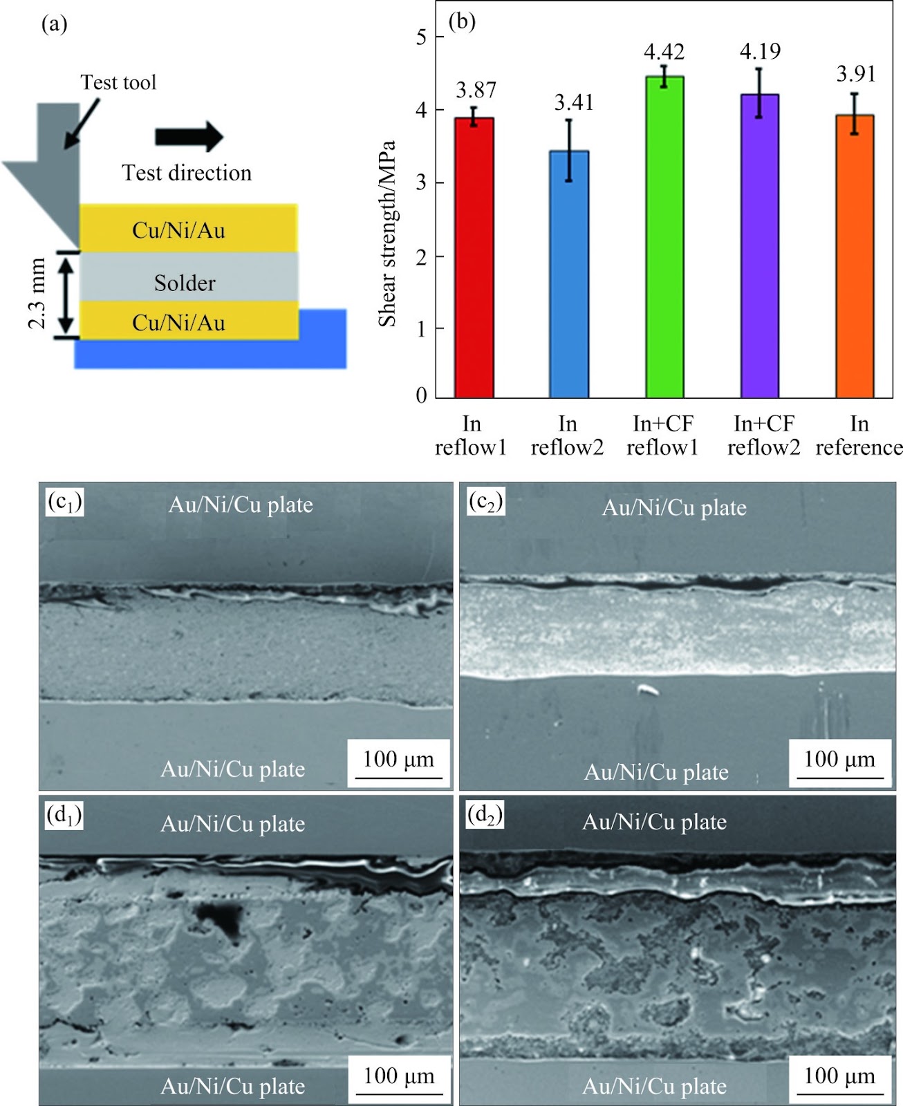
- •• Copper foam (CF) matrix embedded in indium (In) effectively prevents leakage and pump-out of liquid In during multiple reflow cycles in FCBGA packaging, leveraging capillary forces. • The CF matrix promotes the formation of rod-like Cu11In9 at the CF-In interface and inhibits the growth of Ni3In7 IMC at the In-substrate interface, enhancing metallurgical bonding. • The embedded CF matrix improves the shear strength of solder joints by 22.9% and enhances thermal conductivity, while altering fracture behavior from ductile to ductile-brittle mixed type. • This novel TIM1 design eliminates the need for sealants or dams, reducing risks of In explosion and thermal degradation, and avoids additional keep-out zones, offering a more reliable solution for advanced FCBGA packaging.
Abstract
Indium (In) has been used as a thermal interface material (TIM1) in high-performance central processing unit (CPU) for better heat dissipation. However, leakage or pump-out of liquid indium during the multiple reflow cycles limits its application in advanced flip chip ball gray array (FCBGA) packaging. Former researchers place a seal or dam structure to prevent In leakage, leading to the risk of In explosion, thermal degradation, or require additional keep-out zones. In this work, a copper foam (CF) matrix was embedded in In to absorb the liquid In and eliminate the leakage of In TIM1 during the multiple reflow cycles, as the CF capillary force. Au/Ni/Cu-Au/Ni/Cu joint was fabricated by soldering with the composite solder at 190 ℃ for 2 min. After reflow cycles, good metallurgical bonding was formed at interfaces of joint. Rod-like Cu11In9 formed at the CF and In interface, due to the re-dissolved of Cu11In9 crystal. Small amount of Cu atoms from CF can reduce the activity of In, which inhibits the growth of Ni3In7 intermetallic compound (IMC) at the interface of In and Au/Ni/Cu substrate. The CF matrix also improved the shear strength (22.9%) and thermal conductivity of the solder joints. Besides, the fracture behavior of solder joints without CF matrix was classified to be ductile type while that with CF matrix was changed to be ductile-brittle mixed type.
1. Introduction
With the advancement of semiconductor technology, the characteristic dimension of chips has been miniaturized to several nanometers, tens of billions of transistors were integrated into a chip, thus the power density of chips has risen dramatically. Removal of heat from the active semiconductor die and lowering the operation temperature of chip have long been a critical issue to determine logic devices life and speed, especially for high-performance central processing unit (CPU) [1 −3]. The thermal interface material between the die and the lid is defined as TIM1, serving to minimize contact thermal resistance and accommodate the strain from the coefficients of thermal expansion (CTE) mismatch. To meet the heat dissipation requirement of high power CPU, Intel [4] used indium (In) TIM1 to remove heat from chip to lid in land grid array (LGA) packaging and AMD [1] used In TIM1 in pin grid array (PGA) packaging, as the low modulus (12 GPa) and high thermal conductivity (86 W/mK) of In [5]. Figure 1 shows the manufacture processes of flip chip ball gray array (FCBGA) packaging with In TIM1.
Compared with PGA and LGA packaging, ball grid array (BGA) packaging has many advantages, such as smaller size, better heat dissipation and electrical performance [6, 7]. However, the melting point of In (157 ℃) could be a weak point for FCBGA with In TIM1, which needs additional reflow cycles for solder ball (Figure 1(f)) after In TIM1 reflow cycles (Figure 1(d)). In TIM1 remelting could occur during the additional reflow cycles, cause leakage or pump-out of In TIM1 [8]. As the migration of liquid In TIM1 from the up surface to the side of the dies, voids would occur in In TIM1, which could decrease the thermal performance of packaging. And leakage of In TIM1 can also potentially contact adjacent die-side components, creating a short-circuit of components. MCCLURE et al [9] found that voids mainly formed near the center region of the In TIM1 in FCBGA packaging after reflow due to large volume of In extended beyond the die. According to the research reported by LEE et al [10]. In out from the bondline may create extrusion failures. AMD corp. [1] and Intel corp. [4] also revealed the leakage of In.
To prevent In leakage, some solutions proposed by Intel, TSMC and other corporations were used to contain thermal interface materials, such as placing a sealant (Figure 2(a)), a dam (Figure 2(b)) on the integrated circuit device, or incorporating fins (Figure 2(c)) into the integrated heat spreader [11, 12]. However, the sealant and fins on the integrated circuit device form a sealed structure, which could lead to the In explosion phenomenon during reflow. Fins integrated into the heat spreader may also increase costs and create new keep-out zones on the 3821
Loading authentic research manuscript (Pages 1–5)...
WEN Jing, SUN Guo-liao, WANG He-xin, FAN Yi, YI Ming-ming, CHEN Zhuo, WANG Lian-cheng, ZHU Wen-hui (2025). Fabrication and performance of embedded matrix indium thermal interface materials for advanced FCBGA packaging. Journal of Central South University. https://doi.org/10.1007/s11771-025-6052-x
Research & Educational Purpose Only:The translations, structured abstracts, analytical annotations, and data reports provided by SinoTechIntel are intended exclusively for academic research, internal corporate R&D, and educational benchmarking. They do not constitute formal engineering, chemical safety, legal, or professional advice.
Copyright & Intellectual Property Notice: Original copyright of the underlying source articles and experimental data remains with the respective authors, institutions, and original publishing journals. SinoTechIntel claims intellectual property only over its proprietary translations, analytical syntheses, and AEO structured enhancements in accordance with international fair use and academic citation principles.
Frequently Asked Questions
What is the main problem with indium TIM1 in FCBGA packaging?
Indium TIM1 can leak or pump out during multiple reflow cycles due to its low melting point (157°C), leading to voids, reduced thermal performance, and potential short-circuits.
How does the copper foam matrix prevent indium leakage?
The copper foam matrix is embedded in indium and uses capillary forces to absorb and hold the liquid indium, preventing it from leaking or pumping out during reflow cycles.
What are the benefits of using a copper foam matrix in indium TIM1?
The copper foam matrix improves shear strength by 22.9%, enhances thermal conductivity, and changes fracture behavior from ductile to ductile-brittle mixed, while eliminating the need for sealants or dams.
What is the role of Cu11In9 in the solder joint?
Rod-like Cu11In9 forms at the copper foam and indium interface due to re-dissolution, and the small amount of Cu atoms from the foam reduces indium activity, inhibiting the growth of Ni3In7 intermetallic compound at the substrate interface.
How does this new TIM1 design compare to traditional sealant or dam methods?
Unlike sealants or dams, the copper foam matrix avoids the risk of indium explosion, thermal degradation, and additional keep-out zones, offering a more reliable and cost-effective solution for advanced FCBGA packaging.
Related Technical Papers & Translations
Direct Repair of the Crystal Structure and Coating Surface of Spent LiFePO4 Materials Enables Superfast Li-Ion Migration
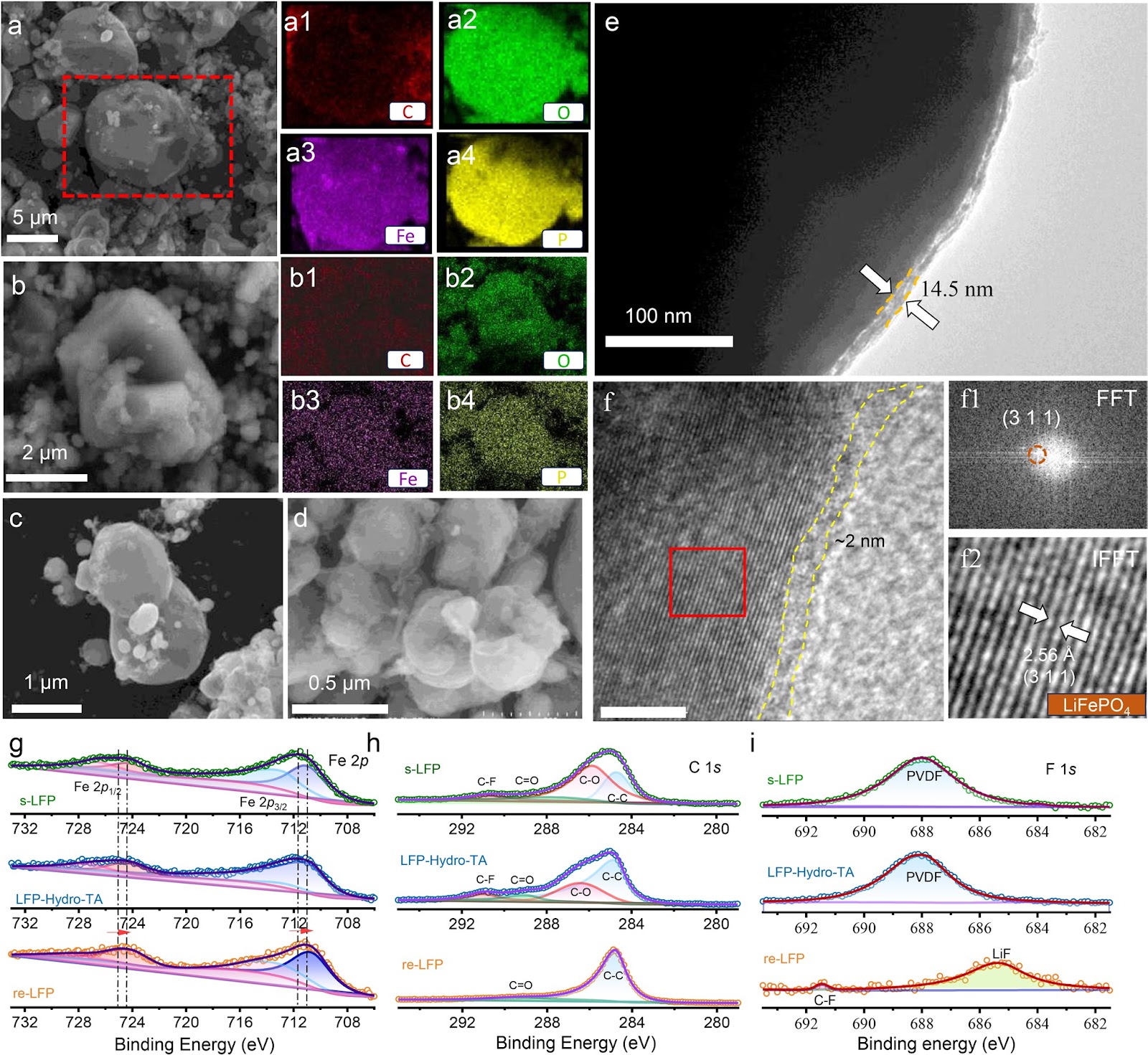
The rapid accumulation of spent LiFePO4 (LFP) cathodes from retired lithium-ion batteries necessitates the development of effective and environmental-friendly recycling strategies. In this context, direct regeneration has emerged as a promising approach for reclaiming LFP cathode materials, offering a streamlined pathway to restore their electrochemical functionality. We report an integrated regeneration protocol that simultaneously repairs the degraded crystal structure and reconstructs the damaged carbon coating in spent LFP. The regenerated cathode material had superfast lithium-ion diffusion kinetics and a stable cathode–electrolyte interface, giving a remarkable rate capability with specific capacities of 122 mAh g−1 at 5C and 106 mAh g−1 at 10C (1C = 170 mA g−1). It also maintained capacities of 110.7 mAh g−1 (5C) and 84.1 mAh g−1 (10C) after 400 cycles. It could be used in harsh environments and could be stably cycled at subzero temperatures (−10 and −20 °C) and in solid-state electrolyte batteries. Life cycle assessment combined with economic evaluation using the EverBatt model reveals that this direct regeneration approach has high economic and environmental benefits.
Oxide Semiconductor for Advanced Memory Architectures: Atomic Layer Deposition, Key Requirement and Challenges
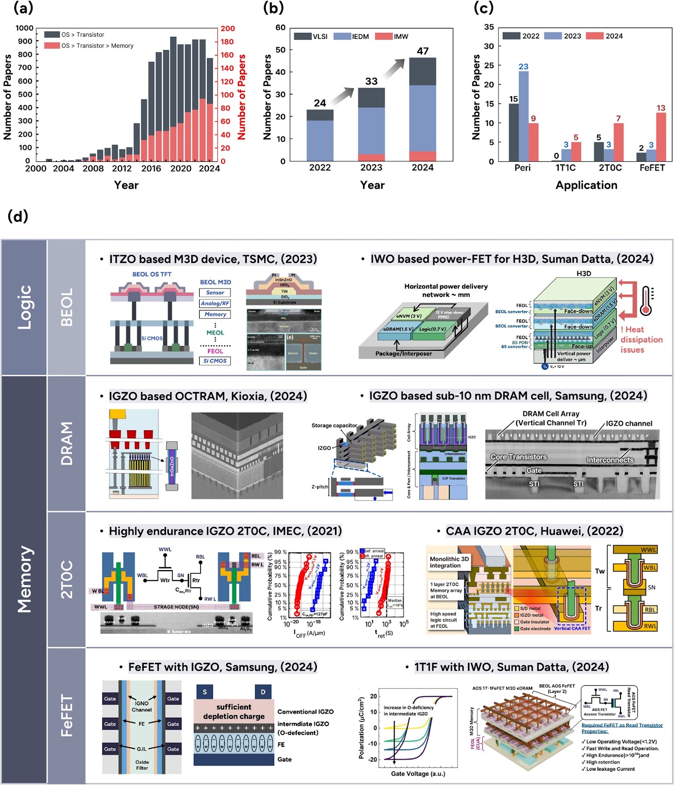
Oxide semiconductors (OSs), introduced by the Hosono group in the early 2000s, have evolved from display backplane materials to promising candidates for advanced memory and logic devices. The exceptionally low leakage current of OSs and compatibility with three-dimensional (3D) architectures have recently sparked renewed interest in their use in semiconductor applications. This review begins by exploring the unique material properties of OSs, which fundamentally originate from their distinct electronic band structure. Subsequently, we focus on atomic layer deposition (ALD), a core technique for growing excellent OS films, covering both basic and advanced processes compatible with 3D scaling. The basic surface reaction mechanisms—adsorption and reaction—and their roles in film growth are introduced. Furthermore, material design strategies, such as cation selection, crystallinity control, anion doping, and heterostructure engineering, are discussed. We also highlight challenges in memory applications, including contact resistance, hydrogen instability, and lack of p-type materials, and discuss the feasibility of ALD-grown OSs as potential solutions. Lastly, we provide an outlook on the role of ALD-grown OSs in memory technologies. This review bridges material fundamentals and device-level requirements, offering a comprehensive perspective on the potential of ALD-driven OSs for next-generation semiconductor memory devices.
Laser powder bed fusion of biodegradable Zn-4Cu alloy: Processing, microstructure and properties
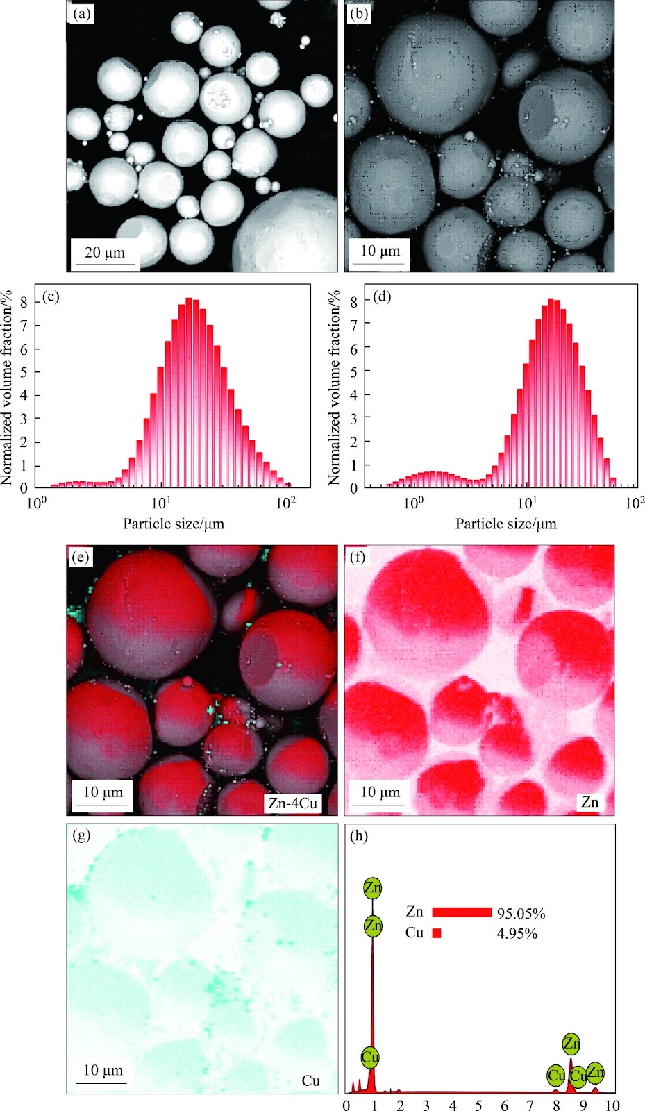
Zn's natural degradability and biocompatibility make it a promising candidate for implants, however, its mechanical properties remain insufficient for bone applications. In this study, the performance of Zn was enhanced by developing Zn-Cu alloys via laser powder bed fusion (LPBF). Optimal LPBF parameters for forming stable tracks were achieved by adjusting laser power and scanning speed. Under optimized conditions of 100 W and 100 mm/s, high-density (99.58%) Zn-Cu alloys with improved hardness (68.2HV) and yield strength (160 MPa) were achieved. These improvements are attributed to solid solution strengthening, segregation strengthening, and grain refinement. The Zn-Cu alloys also demonstrated favorable degradation behavior, with a rate of 0.16 mm/year. This degradation is primarily driven by micro-galvanic corrosion between the CuZn5 phase and Zn matrix, along with refined grains and increased grain boundary density. This work demonstrates a viable strategy for fabricating Zn-based implants with enhanced structural integrity and mechanical performance via LPBF.